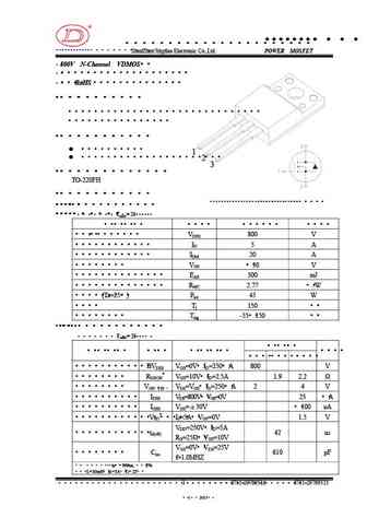
5N80. Аналоги и основные параметры
Наименование производителя: 5N80
Тип транзистора: MOSFET
Полярность: N
Предельные значения
Pd ⓘ - Максимальная рассеиваемая мощность: 125 W
|Vds|ⓘ - Максимально допустимое напряжение сток-исток: 800 V
|Vgs|ⓘ - Максимально допустимое напряжение затвор-исток: 30 V
|Id| ⓘ - Максимально допустимый постоянный ток стока: 5.5 A
Tj ⓘ - Максимальная температура канала: 150 °C
Электрические характеристики
tr ⓘ - Время нарастания: 85 ns
Cossⓘ - Выходная емкость: 100 pf
RDSonⓘ - Сопротивление сток-исток открытого транзистора: 2 Ohm
Тип корпуса: TO-220 TO-220F TO-220F1
Аналог (замена) для 5N80
- подборⓘ MOSFET транзистора по параметрам
5N80 даташит
5n80.pdf
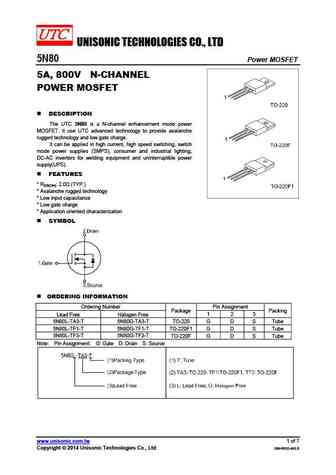
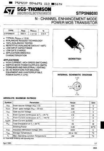
UNISONIC TECHNOLOGIES CO., LTD 5N80 Power MOSFET 5A, 800V N-CHANNEL POWER MOSFET DESCRIPTION The UTC 5N80 is a N-channel enhancement mode power MOSFET. It use UTC advanced technology to provide avalanche rugged technology and low gate charge. It can be applied in high current, high speed switching, switch mode power supplies (SMPS), consumer and industrial lighting,
5n80.pdf
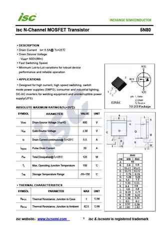
isc N-Channel MOSFET Transistor 5N80 DESCRIPTION Drain Current I = 5.5A@ T =25 D C Drain Source Voltage V = 800V(Min) DSS Fast Switching Speed Minimum Lot-to-Lot variations for robust device performance and reliable operation APPLICATIONS . Designed for high current, high speed switching, switch mode power supplies (SMPS), consumer and industrial lighting, DC-AC
fbm85n80.pdf
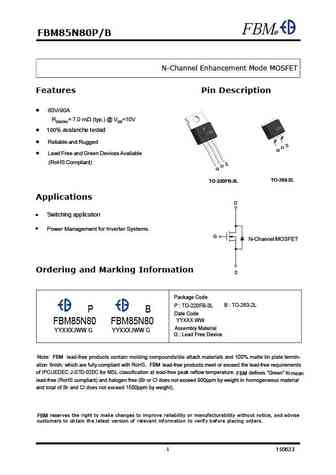
FBM@ FBM85N80P/B N-Channel Enhancement Mode MOSFET Features Pin Description 80V/90A RDS(ON)= 7.0 m (typ.) @ VGS=10V 100% avalanche tested Reliable and Rugged S D G Lead Free and Green Devices Available (RoHS Compliant) S D G TO-263-2L TO-263-2L TO-220FB-3L TO-220FB-3L Applications D Switching application Power Management for Inverter Systems. G N-Channel M
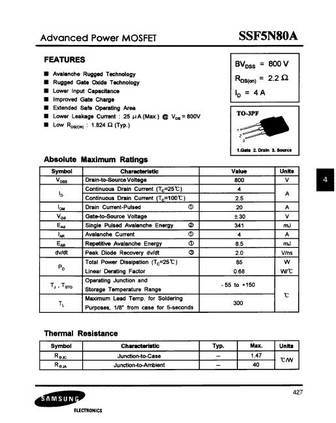
ssh5n80a.pdf
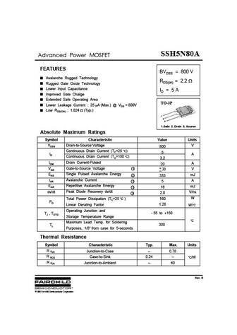
SSH5N80A Advanced Power MOSFET FEATURES BVDSS = 800 V Avalanche Rugged Technology RDS(on) = 2.2 Rugged Gate Oxide Technology Lower Input Capacitance ID = 5 A Improved Gate Charge Extended Safe Operating Area TO-3P Lower Leakage Current 25 A (Max.) @ VDS = 800V Low RDS(ON) 1.824 (Typ.) 1 2 3 1.Gate 2. Drain 3. Source Absolute Maximum Ratings Symbol Charac
ixfh11n80 ixfm11n80 ixfh13n80 ixfm13n80 ixfh14n80 ixfm14n80 ixfh15n80 ixfm15n80.pdf
stf5n80k5.pdf
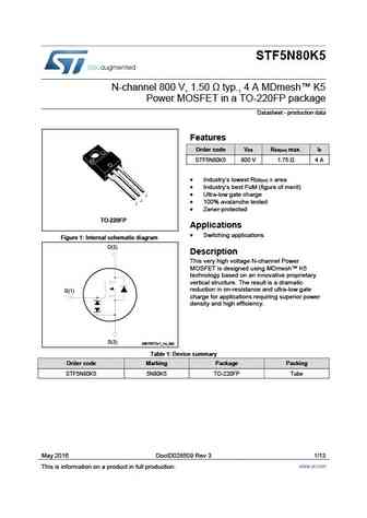
STF5N80K5 N-channel 800 V, 1.50 typ., 4 A MDmesh K5 Power MOSFET in a TO-220FP package Datasheet - production data Features Order code V R max. I DS DS(on) D STF5N80K5 800 V 1.75 4 A Industry s lowest R x area DS(on) Industry s best FoM (figure of merit) Ultra-low gate charge 100% avalanche tested Zener-protected TO-220FP Applications
stb25n80k5 stf25n80k5 stp25n80k5 stw25n80k5.pdf
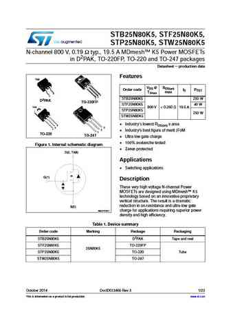
STB25N80K5, STF25N80K5, STP25N80K5, STW25N80K5 N-channel 800 V, 0.19 typ., 19.5 A MDmesh K5 Power MOSFETs in D2PAK, TO-220FP, TO-220 and TO-247 packages Datasheet - production data Features TAB VDS @ RDS(on) Order code ID PTOT TJmax max 3 3 1 2 STB25N80K5 250 W 1 D2PAK TO-220FP STF25N80K5 40 W TAB 800 V
stfu15n80k5.pdf
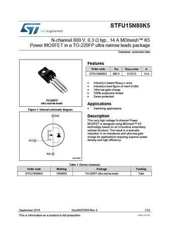
STFU15N80K5 N-channel 800 V, 0.3 typ., 14 A MDmesh K5 Power MOSFET in a TO-220FP ultra narrow leads package Datasheet - production data Features Order code V R max I DS DS(on) D STFU15N80K5 800 V 0.375 14 A Industry s lowest R x area DS(on) Industry s best figure of merit (FoM) Ultra low gate charge 3 2 1 100% avalanche tested Zener-pr
stb15n80k5 stf15n80k5 stp15n80k5 stw15n80k5.pdf
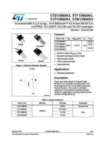
STB15N80K5, STF15N80K5, STP15N80K5, STW15N80K5 N-channel 800 V, 0.3 typ., 14 A MDmesh K5 Power MOSFETs in D2PAK, TO-220FP, TO-220 and TO-247 packages Datasheet - production data Features TAB Order code VDS RDS(on)max ID PTOT 3 STB15N80K5 190 W 1 3 2 STF15N80K5 35 W D2PAK 1 800 V 0.375 14 A TO-220FP STP15N80K5 190 W TAB STW15N80K5 Industry s lowest RDS(on)
stw65n80k5.pdf

STW65N80K5 N-channel 800 V, 0.07 typ., 46 A MDmesh K5 Power MOSFET in a TO-247 package Datasheet - production data Features Order code V R max. I P DS DS(on) D TOT STW65N80K5 800 V 0.08 46 A 446 W Industry s lowest R x area DS(on) Industry s best figure of merit (FoM) 3 Ultra low gate charge 2 100% avalanche tested 1 Zener-protected
fqp5n80.pdf
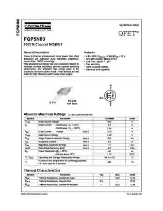
September 2000 TM QFET FQP5N80 800V N-Channel MOSFET General Description Features These N-Channel enhancement mode power field effect 4.8A, 800V, RDS(on) = 2.6 @VGS = 10 V transistors are produced using Fairchild s proprietary, Low gate charge ( typical 25 nC) planar stripe, DMOS technology. Low Crss ( typical 11 pF) This advanced technology has been especially tailor
fqi5n80tu.pdf
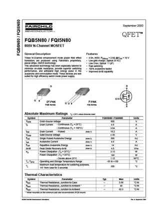
September 2000 TM QFET FQB5N80 / FQI5N80 800V N-Channel MOSFET General Description Features These N-Channel enhancement mode power field effect 4.8A, 800V, RDS(on) = 2.6 @VGS = 10 V transistors are produced using Fairchild s proprietary, Low gate charge ( typical 25 nC) planar stripe, DMOS technology. Low Crss ( typical 11 pF) This advanced technology has been especia
fqpf5n80.pdf
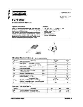
September 2000 TM QFET FQPF5N80 800V N-Channel MOSFET General Description Features These N-Channel enhancement mode power field effect 2.8A, 800V, RDS(on) = 2.6 @VGS = 10 V transistors are produced using Fairchild s proprietary, Low gate charge ( typical 25 nC) planar stripe, DMOS technology. Low Crss ( typical 11 pF) This advanced technology has been especially tailo
ssp5n80a.pdf
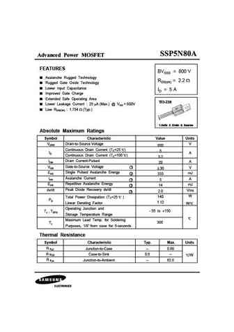
Advanced Power MOSFET FEATURES BVDSS = 800 V Avalanche Rugged Technology RDS(on) = 2.2 Rugged Gate Oxide Technology Lower Input Capacitance ID = 5 A Improved Gate Charge Extended Safe Operating Area Lower Leakage Current 25 A (Max.) @ VDS = 800V Low RDS(ON) 1.754 (Typ.) 1 2 3 1.Gate 2. Drain 3. Source 1.Gate 2. Drain 3. Source Absolute Maximum Ratings S
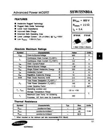
ssw5n80a.pdf
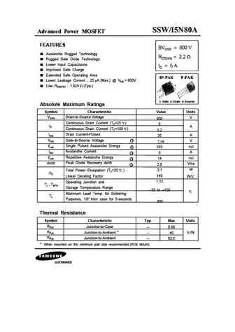
Advanced Power MOSFET FEATURES BVDSS = 800 V Avalanche Rugged Technology RDS(on) = 2.2 Rugged Gate Oxide Technology Lower Input Capacitance ID = 5 A Improved Gate Charge Extended Safe Operating Area Lower Leakage Current 25 A (Max.) @ VDS = 800V 2 Low RDS(ON) 1.824 (Typ.) 1 1 2 3 3 1. Gate 2. Drain 3. Source Absolute Maximum Ratings Symbol Charact
sss5n80a.pdf
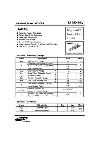
Advanced Power MOSFET FEATURES BVDSS = 800 V Avalanche Rugged Technology RDS(on) = 2.2 Rugged Gate Oxide Technology Lower Input Capacitance ID = 3 A Improved Gate Charge Extended Safe Operating Area Lower Leakage Current 25 A (Max.) @ VDS = 800V Low RDS(ON) 1.824 (Typ.) 1 2 3 1.Gate 2. Drain 3. Source 1.Gate 2. Drain 3. Source Absolute Maximum Ratings S
spw55n80c3.pdf
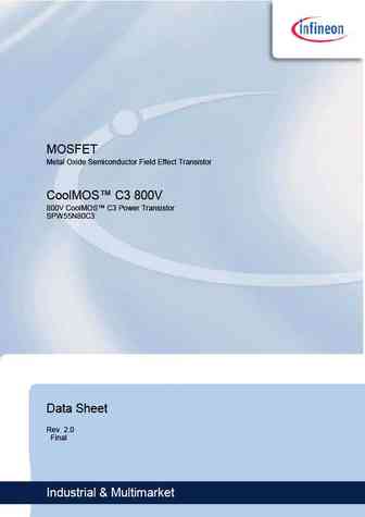
MOSFET Metal Oxide Semiconductor Field Effect Transistor CoolMOS C3 800V 800V CoolMOS C3 Power Transistor SPW55N80C3 Data Sheet Rev. 2.0 Final Industrial & Multimarket 800V CoolMOS C3 Power Transistor SPW55N80C3 TO-247 1 Description 800V CoolMOS C3 designed for Industrial application with high DC bulk voltage Switching Application (i.e. active clamp forward)
ixkr25n80c.pdf
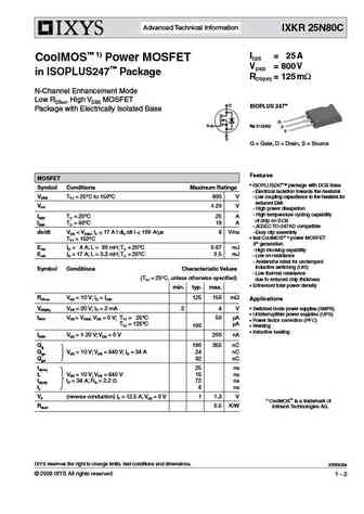
Advanced Technical Information IXKR 25N80C ID25 = 25 A CoolMOS 1) Power MOSFET VDSS = 800 V in ISOPLUS247 Package RDS(on) = 125 mW N-Channel Enhancement Mode Low RDSon, High VDSS MOSFET D ISOPLUS 247 Package with Electrically Isolated Base G G E153432 D S S G = Gate, D = Drain, S = Source Features MOSFET ISOPLUS247 package with DCB Base Symbol Conditions M
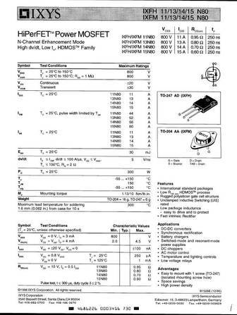
ixfk25n80 ixfk27n80 ixfn25n80 ixfn27n80.pdf
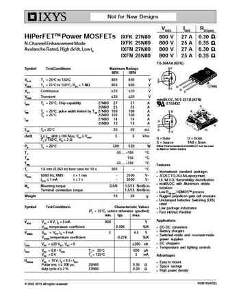
Not for New Designs VDSS ID25 RDS(on) IXFK 27N80 800 V 27 A 0.30 HiPerFETTM Power MOSFETs IXFK 25N80 800 V 25 A 0.35 N-Channel Enhancement Mode Avalanche Rated, High dv/dt, Low trr IXFN 27N80 800 V 27 A 0.30 IXFN 25N80 800 V 25 A 0.35 TO-264 AA (IXFK) Symbol Test Conditions Maximum Ratings
ixfr15n80q.pdf
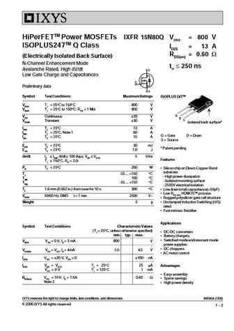
HiPerFETTM Power MOSFETs IXFR 15N80Q VDSS = 800 V ISOPLUS247TM Q Class ID25 = 13 A RDS(on) = 0.60 W (Electrically Isolated Back Surface) N-Channel Enhancement Mode trr 250 ns Avalanche Rated, High dV/dt Low Gate Charge and Capacitances Preliminary data Symbol Test Conditions Maximum Ratings ISOPLUS 247TM VDSS TJ = 25 C to 150 C 800 V VDGR TJ = 25 C to 150 C; RGS = 1 MW 800 V
ixfh15n80q ixft15n80q.pdf
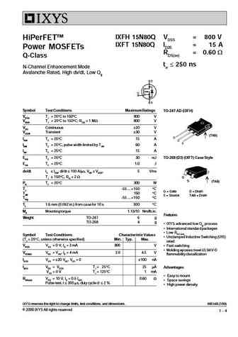
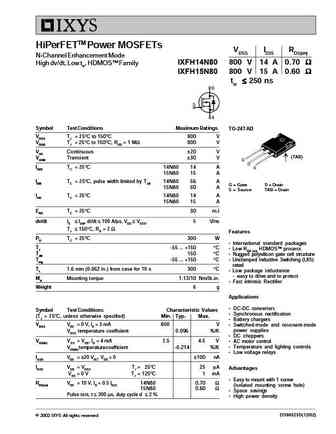
IXFH 15N80Q VDSS = 800 V HiPerFETTM IXFT 15N80Q ID25 = 15 A Power MOSFETs RDS(on) = 0.60 W Q-Class trr 250 ns N-Channel Enhancement Mode Avalanche Rated, High dv/dt, Low Qg Symbol Test Conditions Maximum Ratings TO-247 AD (IXFH) VDSS TJ = 25 C to 150 C 800 V VDGR TJ = 25 C to 150 C; RGS = 1 MW 800 V VGS Continuous 20 V VGSM Transient 30 V (TAB) ID25 TC = 25 C15 A IDM
ixfk27n80 ixfn27n80 ixfk25n80 ixfn25n80.pdf
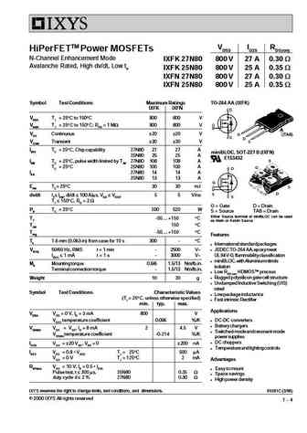
VDSS ID25 RDS(on) HiPerFETTM Power MOSFETs N-Channel Enhancement Mode IXFK 27N80 800 V 27 A 0.30 W Avalanche Rated, High dv/dt, Low trr IXFK 25N80 800 V 25 A 0.35 W IXFN 27N80 800 V 27 A 0.30 W IXFN 25N80 800 V 25 A 0.35 W Symbol Test Conditions Maximum Ratings TO-264 AA (IXFK) IXFK IXFN VDSS TJ = 25 C to 150 C 800 800 V VDGR TJ = 25 C to 150 C; RGS = 1 MW 800 800 V VGS Continuo
ixkg25n80c.pdf
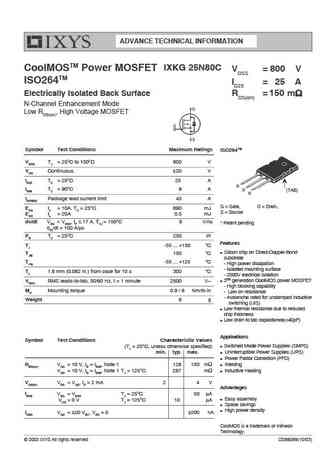
ADVANCE TECHNICAL INFORMATION IXKG 25N80C CoolMOSTM Power MOSFET VDSS = 800 V ISO264TM ID25 = 25 A Electrically Isolated Back Surface RDS(on) = 150 m N-Channel Enhancement Mode Low RDS(on), High Voltage MOSFET Symbol Test Conditions Maximum Ratings ISO264TM VDSS TJ = 25 C to 150 C 800 V VGS Continuous 20 V ID25 TC = 25 C 25 A G ID90 TC = 90 C 9 A D
fdb0165n807l.pdf

Is Now Part of To learn more about ON Semiconductor, please visit our website at www.onsemi.com Please note As part of the Fairchild Semiconductor integration, some of the Fairchild orderable part numbers will need to change in order to meet ON Semiconductor s system requirements. Since the ON Semiconductor product management systems do not have the ability to manage part nomenclatur
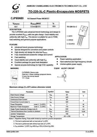
cjp75n80.pdf
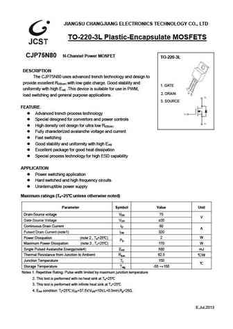
JIANGSU CHANGJIANG ELECTRONICS TECHNOLOGY CO., LTD TO-220-3L Plastic-Encapsulate MOSFETS CJP75N80 N-Channel Power MOSFET TO-220-3L DESCRIPTION The CJP75N80 uses advanced trench technology and design to provide excellent RDS(on) with low gate charge. Good stability and 1. GATE uniformity with high EAS .This device is suitable for use in PWM, 2. DRAIN load switching and gen
cjp85n80.pdf
JIANGSU CHANGJIANG ELECTRONICS TECHNOLOGY CO., LTD TO-220-3L-C Plastic-Encapsulate MOSFETS CJP85N80 N-Channel Power MOSFET ID V (BR)DSS RDS(on)MAX 80A 8.5m @10V 85V TO-220-3L-C DESCRIPTION The CJP85N80 uses advanced trench technology and design to provide excellent RDS(on) with low gate charge. Good stability and 1. GATE uniformity with high EAS .This device is suitab
sff15n80.pdf
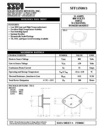
SFF15N80/3 SOLID STATE DEVICES, INC. 14830 Valley View Blvd * La Mirada, Ca 90638 Phone (562) 404-7855 * Fax (562) 404-1773 ssdi@ssdi-power.com * www.ssdi-power.com 15 AMPS 800 VOLTS DESIGNER'S DATA SHEET 0.60 N-CHANNEL FEATURES POWER MOSFET Low RDS (on) and High Transconductance Excellent High Temperature Stability TO-3 Fast Switching Speed Intrinsic Rectifi
hfp75n80c.pdf
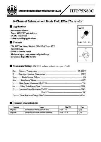
Shantou Huashan Electronic Devices Co.,Ltd. HFP75N80C N-Channel Enhancement Mode Field Effect Transistor Applications TO-220 Servo motor control. Power MOSFET gate drivers. DC/DC converters Other switching applications. 1- G 2-D 3-S Features 75A, 80V(See Note), RDS(on)
hfp5n80.pdf
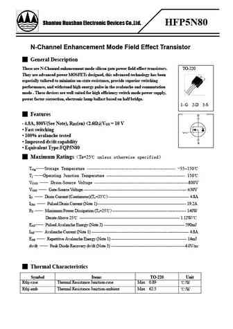
Shantou Huashan Electronic Devices Co.,Ltd. HFP5N80 N-Channel Enhancement Mode Field Effect Transistor General Description These are N-Channel enhancement mode silicon gate power field effect transistors. TO-220 They are advanced power MOSFETs designed, this advanced technology has been especially tailored to minimize on-state resistance, provide superior switching performanc
ftk5n80p f dd.pdf
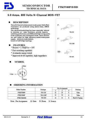
SEMICONDUCTOR FTK5N80P/D/DD TECHNICAL DATA 5.0 Amps, 800 Volts N-Channel MOS-FET DESCRIPTION These N-Channel enhancement mode power field effect P Transistors are produced using planar stripe, DMOS technology. 1 This advanced technology has been especially tailored to minimize on - state resistance , provide superior TO-220 switching performance,and Withstand high energy pulse in
f5n80.pdf
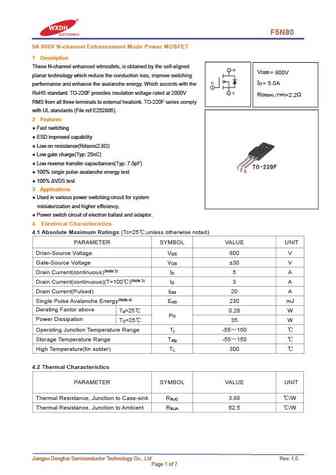
F5N80 5A 800V N-channel Enhancement Mode Power MOSFET 1 Description These N-channel enhanced vdmosfets, is obtained by the self-aligned V DSS = 800V planar technology which reduce the conduction loss, improve switching I = 5.0A D performance and enhance the avalanche energy. Which accords with the RoHS standard. TO-220F provides insulation voltage rated at 2000V R DS(on) TYP) =2.
wfp5n80.pdf
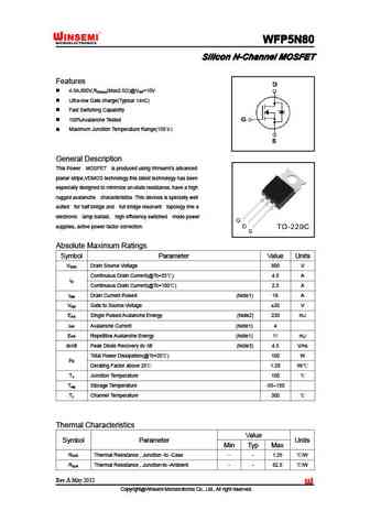
WFP5N80 WFP5N80 WFP5N80 WFP5N80 Silicon N-Channel MOSFET Silicon N-Channel MOSFET Silicon N-Channel MOSFET Silicon N-Channel MOSFET Features 4.5A,800V,R (Max2.5 )@V =10V DS(on) GS Ultra-low Gate charge(Typical 14nC) Fast Switching Capability 100%Avalanche Tested Maximum Junction Temperature Range(150 ) General Description This Power MOSFET is produced usi
wff5n80.pdf
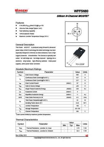
WFF5N80 WFF5N80 WFF5N80 WFF5N80 Silicon N-Channel MOSFET Silicon N-Channel MOSFET Silicon N-Channel MOSFET Silicon N-Channel MOSFET Features 4.5A,800V,R (Max2.5 )@V =10V DS(on) GS Ultra-low Gate charge(Typical 14nC) Fast Switching Capability 100%Avalanche Tested Maximum Junction Temperature Range(150 ) General Description This Power MOSFET is produced usi
jfpc5n80c jffm5n80c.pdf
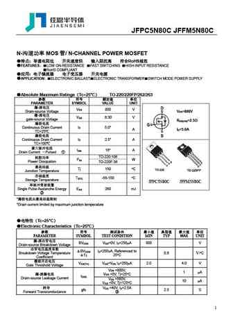
JFPC5N80C JFFM5N80C N- MOS / N-CHANNEL POWER MOSFET RoHS FEATURES LOW ON-RESISTANCE FAST SWITCHING HIGH INPUT RESISTANCE RoHS COMPLIANT APPLICATION ELECTRONIC BALLAST ELECTRONIC TRANSFORMER SWITCH MODE POWER SUP
nce65n800d.pdf
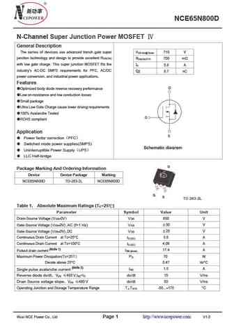
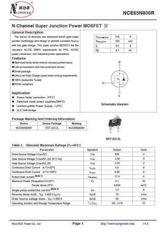
NCE65N800D N-Channel Super Junction Power MOSFET General Description The series of devices use advanced trench gate super V 710 V DS min@Tjmax junction technology and design to provide excellent RDS(ON) R 700 m DS(ON)TYP. with low gate charge. This super junction MOSFET fits the I 5.8 A D industry s AC-DC SMPS requirements for PFC, AC/DC Qg 8.7 nC power conversion, and indu
nce65n800k.pdf
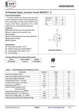
NCE65N800K N-Channel Super Junction Power MOSFET General Description The series of devices use advanced trench gate super V 710 V DS min@Tjmax junction technology and design to provide excellent RDS(ON) R 700 m DS(ON)TYP. with low gate charge. This super junction MOSFET fits the I 5.8 A D industry s AC-DC SMPS requirements for PFC, AC/DC Qg 8.7 nC power conversion, and indu
nce65n800r.pdf
NCE65N800R N-Channel Super Junction Power MOSFET General Description The series of devices use advanced trench gate super V 710 V DS min@Tjmax junction technology and design to provide excellent RDS(ON) R 700 m DS(ON)TYP. with low gate charge. This super junction MOSFET fits the I 5.8 A D industry s AC-DC SMPS requirements for PFC, AC/DC Qg 8.7 nC power conversion, and indu
nce65n800f.pdf

NCE65N800F N-Channel Super Junction Power MOSFET General Description The series of devices use advanced trench gate super V 710 V DS min@Tjmax junction technology and design to provide excellent RDS(ON) R 700 m DS(ON)TYP. with low gate charge. This super junction MOSFET fits the I 5.8 A D industry s AC-DC SMPS requirements for PFC, AC/DC Qg 8.7 nC power conversion, and indu
nce65n800i.pdf

NCE65N800I N-Channel Super Junction Power MOSFET General Description The series of devices use advanced trench gate super V 710 V DS min@Tjmax junction technology and design to provide excellent RDS(ON) R 700 m DS(ON)TYP. with low gate charge. This super junction MOSFET fits the I 5.8 A D industry s AC-DC SMPS requirements for PFC, AC/DC Qg 8.7 nC power conversion, and indu
hfs5n80.pdf
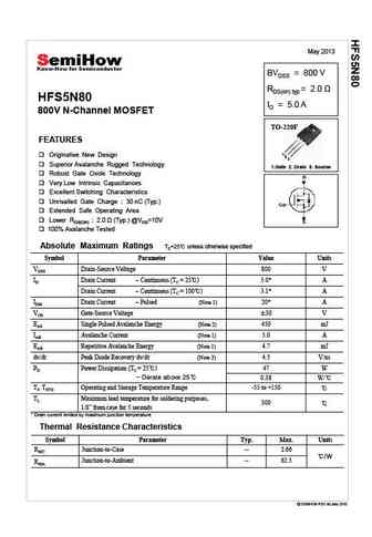
May 2013 BVDSS = 800 V RDS(on) typ HFS5N80 ID = 5.0 A 800V N-Channel MOSFET TO-220F FEATURES 1 1 Originative New Design 2 3 Superior Avalanche Rugged Technology 1.Gate 2. Drain 3. Source Robust Gate Oxide Technology Very Low Intrinsic Capacitances Excellent Switching Characteristics Unrivalled Gate Charge 30 nC (Typ.) Extended Safe Operating Area
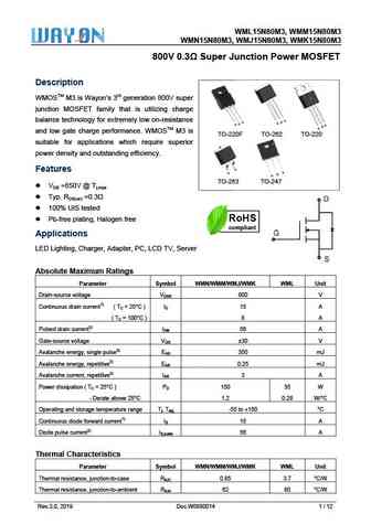
wml05n80m3 wmn05n80m3 wmm05n80m3 wmo05n80m3 wmp05n80m3 wmk05n80m3.pdf
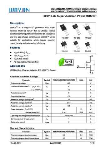
WML05N80M3, W 80M3, WM M3 WMN05N8 MM05N80M WMO0 80M3, WM M3 05N80M3, WMP05N8 MK05N80M 800 Junction ET 0V 2.0 Super J n Power MOSFE Descrip ption WMOSTM M3 is Wayo neration 800 M on s 3rd gen 0V super junction MOSFET fa that is utilizing charge M amily S balance te or extremely esistance D echnology fo y low on-re S S G D D G G G T and low ga charge perf
wml25n80m3 wmm25n80m3 wmn25n80m3 wmj25n80m3 wmk25n80m3.pdf
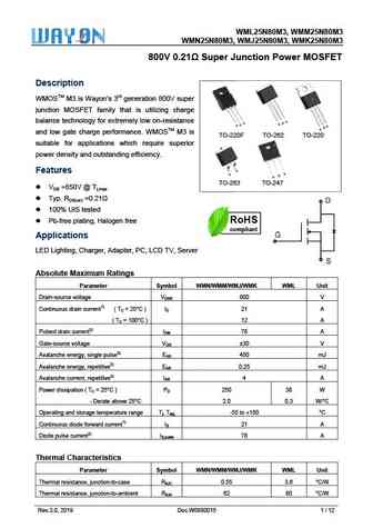
WML25N8 MM25N80M 80M3, WM M3 WMN2 80M3, WM M3 25N80M3, WMJ25N8 MK25N80M 800V 0.21 S T V Super Junction Power MOSFET Descrip ption WMOSTM M3 is Wayo neration 800 M on s 3rd gen 0V super junction MOSFET fa that is utilizing charge M amily S balance te or extremely esistance echnology fo y low on-re S D D G G G S D G T and low ga charge performanc WMOSTM
wml15n80m3 wmm15n80m3 wmn15n80m3 wmj15n80m3 wmk15n80m3.pdf
WML15N8 MM15N80M 80M3, WM M3 WMN1 80M3, WM M3 15N80M3, WMJ15N8 MK15N80M 800V 0.3 S T Super Junction Power MOSFET Descrip ption WMOSTM M3 is Wayo neration 800 M on s 3rd gen 0V super junction MOSFET fa that is utilizing charge M amily S balance te or extremely esistance echnology fo y low on-re S D D G G G S D G T and low ga charge performanc WMOSTM M3
cs5n80f cs5n80p cs5n80b.pdf
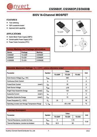
nvert Suzhou Convert Semiconductor Co ., Ltd. CS5N80F, CS5N80P,CS5N80B 800V N-Channel MOSFET FEATURES Fast switching 100% avalanche tested Improved dv/dt capability APPLICATIONS Switch Mode Power Supply (SMPS) Uninterruptible Power Supply (UPS) Power Factor Correction (PFC) Device Marking and Package Information Device Package Marking CS5N80F TO-220F CS5N80
cs5n80f cs5n80p.pdf
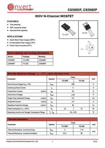
nvert Suzhou Convert Semiconductor Co ., Ltd. CS5N80F, CS5N80P 800V N-Channel MOSFET FEATURES Fast switching 100% avalanche tested Improved dv/dt capability APPLICATIONS Switch Mode Power Supply (SMPS) Uninterruptible Power Supply (UPS) Power Factor Correction (PFC) Device Marking and Package Information Device Package Marking CS5N80F TO-220F CS5N80F CS5N8
fir5n80fg.pdf
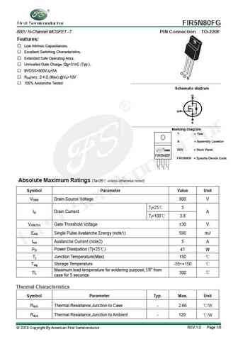
FIR5N80FG 800V N-Channel MOSFET -T PIN Connection TO-220F Features Low Intrinsic Capacitances. Excellent Switching Characteristics. Extended Safe Operating Area. Unrivalled Gate Charge Qg=31nC (Typ.). BVDSS=800V,ID=5A G D S RDS(on) 2.4 (Max) @VG=10V 100% Avalanche Tested g Schematic dia ram D G S Marking Diagram Y = Year A = Assembl
vbzm75n80.pdf
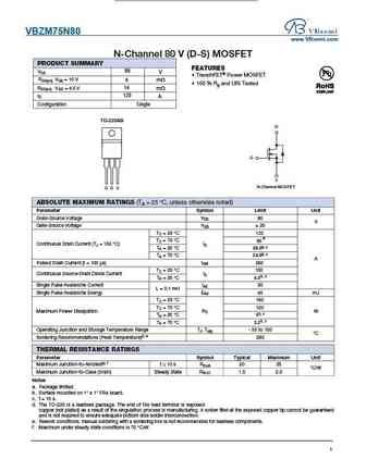
VBZM75N80 www.VBsemi.com N-Channel 80 V (D-S) MOSFET PRODUCT SUMMARY FEATURES 80 VDS V TrenchFET Power MOSFET RDS(on) VGS = 10 V 6 m 100 % Rg and UIS Tested RDS(on) VGS = 4.5 V 14 m 120 ID A Configuration Single TO-220AB D G S N-Channel MOSFET G D S ABSOLUTE MAXIMUM RATINGS (TA = 25 C, unless otherwise noted) Parameter Symbol Limit Unit Drain-Sourc
hm85n80.pdf
N-Channel Enhancement Mode Power MOSFET Description The uses advanced trench technology and design to provide excellent RDS(ON) with low gate charge. This device is suitable for use in PWM, load switching and general purpose applications. General Features VDS =85V,ID =80A Schematic diagram RDS(ON)
hm75n80.pdf
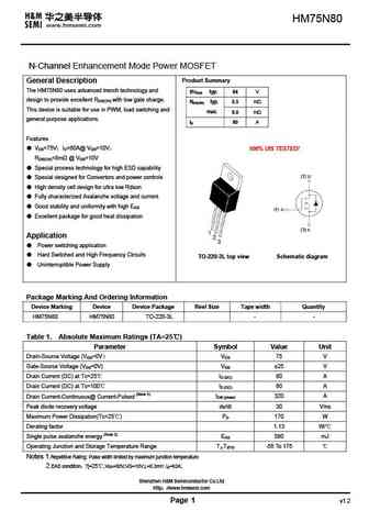
HM75N80 N-Channel Enhancement Mode Power MOSFET Product Summary General Description The HM75N80 uses advanced trench technology and BVDSS typ. 84 V design to provide excellent RDS(ON) with low gate charge. RDS(ON) typ. 6.5 m This device is suitable for use in PWM, load switching and max. 8.0 m general purpose applications. ID 80 A Features VDS=75V ID=80
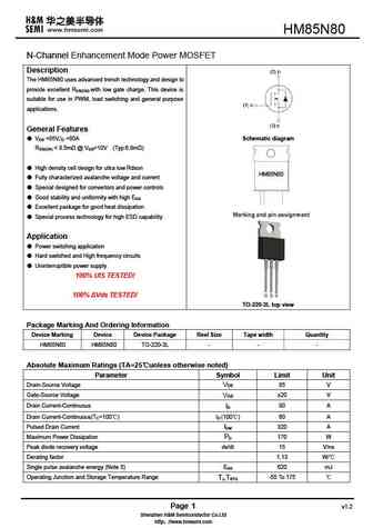
hm75n80d.pdf
HM75N80D N-Channel Enhancement Mode Power MOSFET Description The HM75N80D uses advanced trench technology and design to provide excellent RDS(ON) with low gate charge. This device is suitable for use in PWM, load switching and general purpose applications. General Features VDS = 75V,ID =80A Schematic diagram RDS(ON)
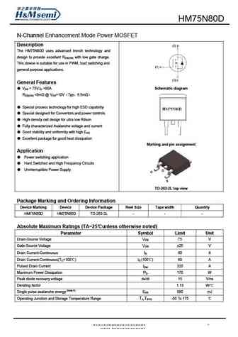
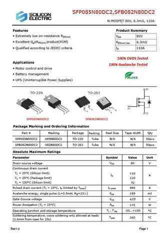
sfd085n80c2.pdf
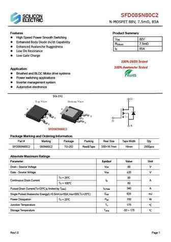
SFD085N80C2 N-MOSFET 80V, 7.5m , 85A Features Product Summary High Speed Power Smooth Switching V 80V DS Enhanced Body Diode dv/dt Capability R 7.5m DS(on) Enhanced Avalanche Ruggedness I 85A D Low On Resistance Low Gate Charge 100% DVDS Tested 100% Avalanche Tested Application Brushed and BLDC Motor drive systems Power switching applic
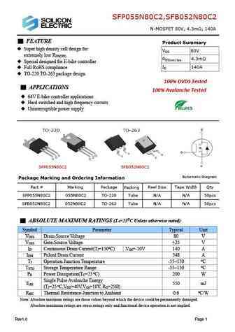
sfp085n80dc2 sfb082n80dc2.pdf
SFP085N80DC2,SFB082N80DC2 N-MOSFET 80V, 6.3m , 110A Features Product Summary Extremely low on-resistance RDS(on) VDS 80V Excellent QgxRDS(on) product(FOM) RDS(on) typ. 6.3m Qualified according to JEDEC criteria ID 110A 100% DVDS Tested Applications 100% Avalanche Tested Motor control and drive Battery management UPS (Uninterrupible Power Supplies) S
stf5n80k5.pdf
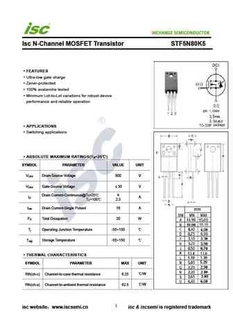
INCHANGE Semiconductor Isc N-Channel MOSFET Transistor STF5N80K5 FEATURES Ultra-low gate charge Zener-protected 100% avalanche tested Minimum Lot-to-Lot variations for robust device performance and reliable operation APPLICATIONS Switching applications ABSOLUTE MAXIMUM RATINGS(T =25 ) a SYMBOL PARAMETER VALUE UNIT V Drain-Source Voltage 800 V DSS V Gate-Source V
stb15n80k5.pdf
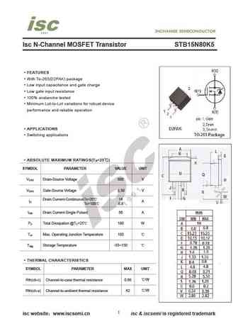
Isc N-Channel MOSFET Transistor STB15N80K5 FEATURES With To-263(D2PAK) package Low input capacitance and gate charge Low gate input resistance 100% avalanche tested Minimum Lot-to-Lot variations for robust device performance and reliable operation APPLICATIONS Switching applications ABSOLUTE MAXIMUM RATINGS(T =25 ) a SYMBOL PARAMETER VALUE UNIT V Drain-Source Vo
Другие MOSFET... 4N90 , 5N90 , 6N90 , 7N90 , 1N80 , 2N80 , 3N80 , 4N80 , AON7408 , 6N80 , 7N80 , 8N80 , 9N80 , 10N80 , 12N80 , 1N70Z , 2N70 .
🌐 : EN ES РУ

Список транзисторов
Обновления
MOSFET: ASD80R750E | ASD70R950E | ASD70R600E | ASD70R380E | ASD65R850E | ASD65R550E | ASD65R350E | ASD65R300E | ASD65R280E | ASD65R270E | ASD60R330E | ASD60R280E | ASB80R750E | ASB70R380E | ASB65R300E | ASB65R220E
Popular searches
irf540 equivalent | mp1620 transistor equivalent | 2sc945 transistor | c2073 transistor | ac176 transistor | mpsa20 | irfp264 | ksc2690