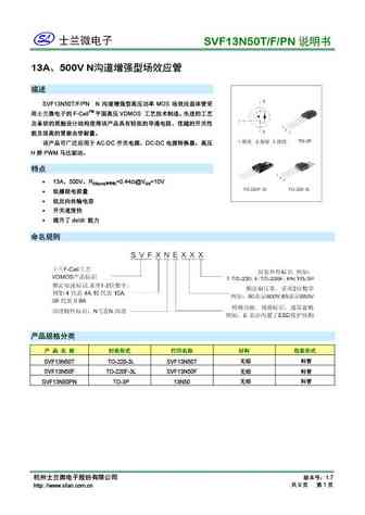
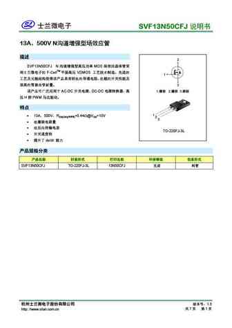
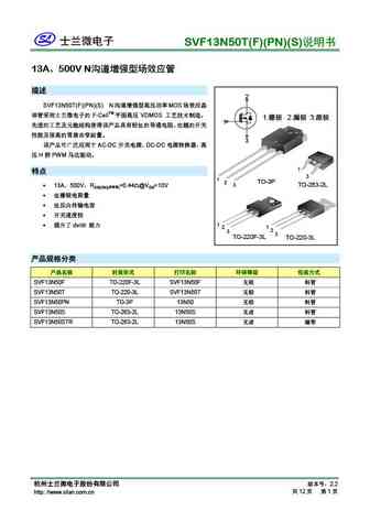
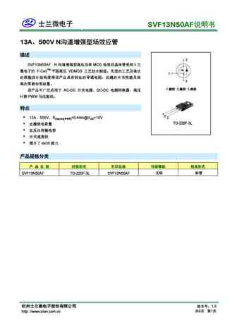
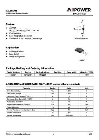
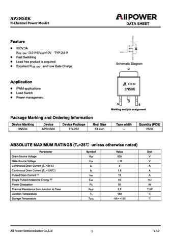
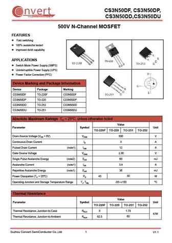
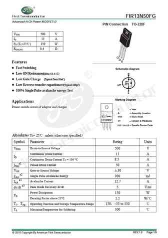
3N50. Аналоги и основные параметры
Наименование производителя: 3N50
Тип транзистора: MOSFET
Полярность: N
Предельные значения
Pd ⓘ - Максимальная рассеиваемая мощность: 50 W
|Vds|ⓘ - Предельно допустимое напряжение сток-исток: 500 V
|Vgs|ⓘ - Предельно допустимое напряжение затвор-исток: 30 V
|Id| ⓘ - Максимально допустимый постоянный ток стока: 3 A
Tj ⓘ - Максимальная температура канала: 150 °C
Электрические характеристики
tr ⓘ - Время нарастания: 25 ns
Cossⓘ - Выходная емкость: 50 pf
Rds ⓘ - Сопротивление сток-исток открытого транзистора: 2.2 Ohm
Аналог (замена) для 3N50
3N50 даташит
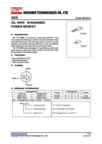
3n50.pdf
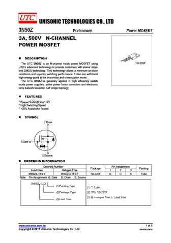
UNISONIC TECHNOLOGIES CO., LTD 3N50 Power MOSFET 3A, 500V N-CHANNEL POWER MOSFET 1 TO-220F DESCRIPTION The UTC 3N50 is an N-channel mode power MOSFET using UTC s advanced technology to provide customers with planar stripe and DMOS technology. This technology allows a minimum on-state 1 resistance and superior switching performance. It also can withstand high energy pulse
3n50.pdf
isc N-Channel MOSFET Transistor 3N50 FEATURES Drain Current I = 3A@ T =25 D C Drain Source Voltage- V = 500V(Min) DSS Static Drain-Source On-Resistance R = 3.0 (Max) DS(on) Fast Switching Minimum Lot-to-Lot variations for robust device performance and reliable operation APPLICATIONS Switching power supplies,converters,AC and DC motor controls ABSOLUTE M
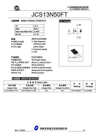
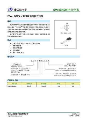
jcs13n50ft.pdf
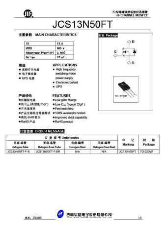
N N- CHANNEL MOSFET R JCS13N50FT MAIN CHARACTERISTICS Package ID 13 A VDSS 500 V Rdson-max @Vgs=10V 0.46 Qg-typ 37 nC APPLICATIONS High frequency switching mode power supply UPS Electronic ballast UPS FEATUR
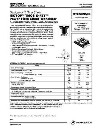
mte53n50e.pdf
MOTOROLA Order this document SEMICONDUCTOR TECHNICAL DATA by MTE53N50E/D Designer's Data Sheet MTE53N50E ISOTOP TMOS E-FET. Motorola Preferred Device Power Field Effect Transistor N Channel Enhancement Mode Silicon Gate TMOS POWER FET 53 AMPERES This advanced high voltage TMOS E FET is designed to 500 VOLTS withstand high energy in the avalanche mode and switch effi
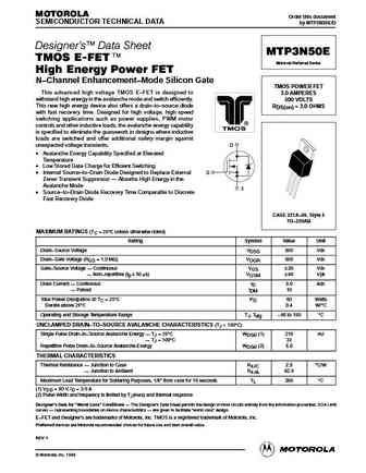
mtp3n50e.pdf
MOTOROLA Order this document SEMICONDUCTOR TECHNICAL DATA by MTP3N50E/D Designer's Data Sheet MTP3N50E TMOS E-FET. Motorola Preferred Device High Energy Power FET N Channel Enhancement Mode Silicon Gate TMOS POWER FET This advanced high voltage TMOS E FET is designed to 3.0 AMPERES withstand high energy in the avalanche mode and switch efficiently. 500 VOLTS This new
mtp3n50erev1a.pdf
MOTOROLA Order this document SEMICONDUCTOR TECHNICAL DATA by MTP3N50E/D Designer's Data Sheet MTP3N50E TMOS E-FET. Motorola Preferred Device High Energy Power FET N Channel Enhancement Mode Silicon Gate TMOS POWER FET This advanced high voltage TMOS E FET is designed to 3.0 AMPERES withstand high energy in the avalanche mode and switch efficiently. 500 VOLTS This new
mte53n50erev2.pdf
MOTOROLA Order this document SEMICONDUCTOR TECHNICAL DATA by MTE53N50E/D Designer's Data Sheet MTE53N50E ISOTOP TMOS E-FET. Motorola Preferred Device Power Field Effect Transistor N Channel Enhancement Mode Silicon Gate TMOS POWER FET 53 AMPERES This advanced high voltage TMOS E FET is designed to 500 VOLTS withstand high energy in the avalanche mode and switch effi
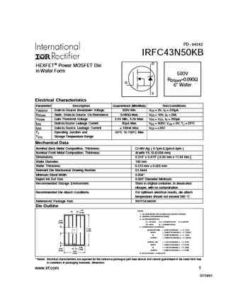
irfc43n50kb.pdf
PD - 94242 IRFC43N50KB D HEXFET Power MOSFET Die in Wafer Form 500V RDS(on)=0.090 G 6" Wafer S Electrical Characteristics Parameter Description Guaranteed (Min/Max) Test Conditions V(BR)DSS Drain-to-Source Breakdown Voltage 500V Min. VGS = 0V, ID = 250 A RDS(on) Static Drain-to-Source On-Resistance 0.090 Max. VGS = 10V, ID = 28A VGS(th) Gate Threshold Voltage 3.0V Min., 5
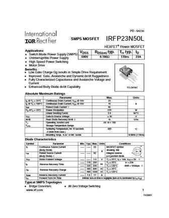
irfp23n50l.pdf
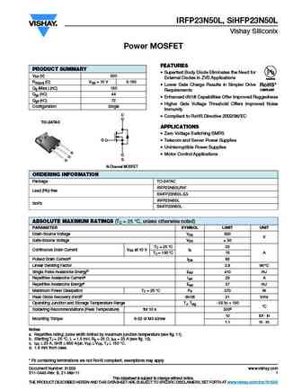
PD - 94230 SMPS MOSFET IRFP23N50L HEXFET Power MOSFET Applications VDSS RDS(on) typ. Trr typ. ID Switch Mode Power Supply (SMPS) 500V 0.190 170ns 23A UninterruptIble Power Supply High Speed Power Switching Motor Drive Benefits Low Gate Charge Qg results in Simple Drive Requirement Improved Gate, Avalanche and Dynamicdv/dt Ruggedness Fully Characterized Capacitance and
irfps43n50kpbf.pdf
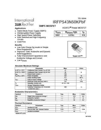
PD- 95898 IRFPS43N50KPbF SMPS MOSFET HEXFET Power MOSFET Applications l Switch Mode Power Supply (SMPS) VDSS RDS(on) typ. ID l Uninterruptible Power Supply l High Speed Power Switching 500V 0.078 47A l Hard Switched and High Frequency Circuits l Lead-Free Benefits l Low Gate Charge Qg results in Simple Drive Requirement l Improved Gate, Avalanche and Dynamic dv/dt Ruggednes
irfps43n50k.pdf
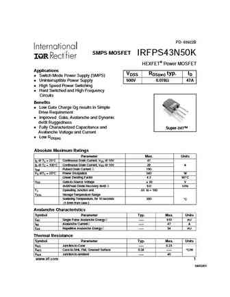
PD- 93922B SMPS MOSFET IRFPS43N50K HEXFET Power MOSFET Applications VDSS RDS(on) typ. ID Switch Mode Power Supply (SMPS) Uninterruptible Power Supply 500V 0.078 47A High Speed Power Switching Hard Switched and High Frequency Circuits Benefits Low Gate Charge Qg results in Simple Drive Requirement Improved Gate, Avalanche and Dynamic dv/dt Ruggedness Fully Characteriz
irfb13n50apbf.pdf
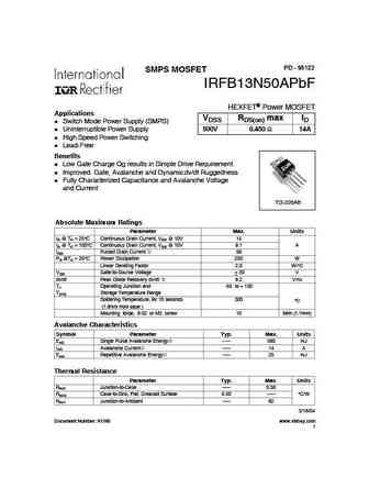
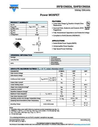
PD - 95122 SMPS MOSFET IRFB13N50APbF HEXFET Power MOSFET AppIications VDSS RDS(on) max ID l Switch Mode Power Supply (SMPS) l Uninterruptible Power Supply 500V 0.450 14A l High Speed Power Switching l Lead-Free Benefits l Low Gate Charge Qg results in Simple Drive Requirement l Improved Gate, Avalanche and Dynamicdv/dt Ruggedness l Fully Characterized Capacitance and Avalanch
irfb13n50a.pdf
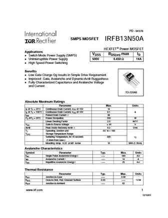
PD - 94339 SMPS MOSFET IRFB13N50A HEXFET Power MOSFET Applications VDSS RDS(on) max ID Switch Mode Power Supply (SMPS) Uninterruptible Power Supply 500V 0.450 14A High Speed Power Switching Benefits Low Gate Charge Qg results in Simple Drive Requirement Improved Gate, Avalanche and Dynamicdv/dt Ruggedness Fully Characterized Capacitance and Avalanche Voltage and Current
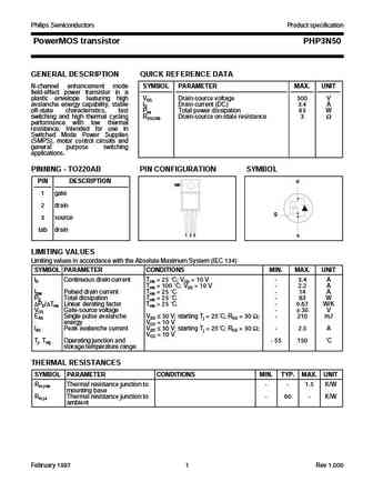
php3n50 1.pdf
Philips Semiconductors Product specification PowerMOS transistor PHP3N50 GENERAL DESCRIPTION QUICK REFERENCE DATA N-channel enhancement mode SYMBOL PARAMETER MAX. UNIT field-effect power transistor in a plastic envelope featuring high VDS Drain-source voltage 500 V avalanche energy capability, stable ID Drain current (DC) 3.4 A off-state characteristics, fast Ptot Total power dissipati
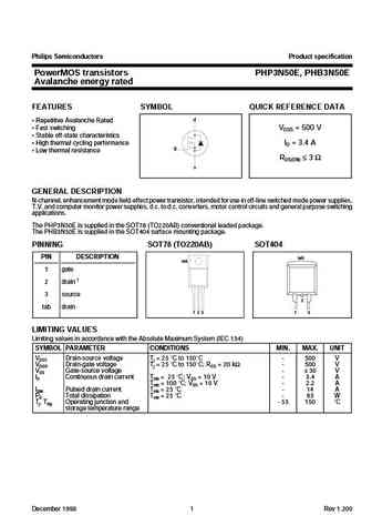
php3n50e phb3n50e.pdf
Philips Semiconductors Product specification PowerMOS transistors PHP3N50E, PHB3N50E Avalanche energy rated FEATURES SYMBOL QUICK REFERENCE DATA d Repetitive Avalanche Rated Fast switching VDSS = 500 V Stable off-state characteristics High thermal cycling performance ID = 3.4 A g Low thermal resistance RDS(ON) 3 s GENERAL DESCRIPTION N-channel, enhan
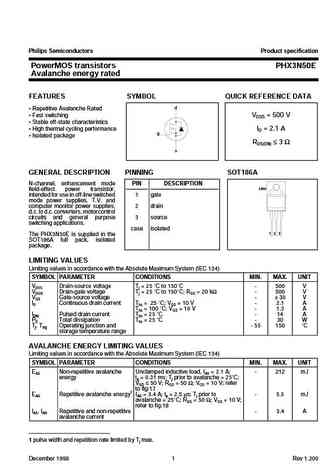
phx3n50e.pdf
Philips Semiconductors Product specification PowerMOS transistors PHX3N50E Avalanche energy rated FEATURES SYMBOL QUICK REFERENCE DATA d Repetitive Avalanche Rated Fast switching VDSS = 500 V Stable off-state characteristics High thermal cycling performance ID = 2.1 A g Isolated package RDS(ON) 3 s GENERAL DESCRIPTION PINNING SOT186A N-channel, enhan
std13n50dm2ag.pdf
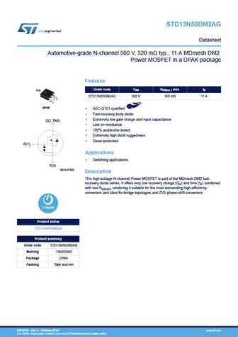
STD13N50DM2AG Datasheet Automotive-grade N-channel 500 V, 320 m typ., 11 A MDmesh DM2 Power MOSFET in a DPAK package Features VDS RDS(on ) max. ID Order code TAB STD13N50DM2AG 500 V 360 m 11 A 3 2 1 DPAK AEC-Q101 qualified Fast-recovery body diode Extremely low gate charge and input capacitance D(2, TAB) Low on-resistance 100% avalanche tested E
fqb13n50ctm fqb13n50c fqi13n50c fqi13n50ctu.pdf
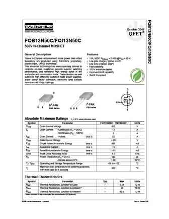
October 2008 QFET FQB13N50C/FQI13N50C 500V N-Channel MOSFET General Description Features These N-Channel enhancement mode power field effect 13A, 500V, RDS(on) = 0.48 @VGS = 10 V transistors are produced using Fairchild s proprietary, Low gate charge ( typical 43nC) planar stripe, DMOS technology. Low Crss ( typical 20pF) This advanced technology has been especially
fqa13n50c.pdf
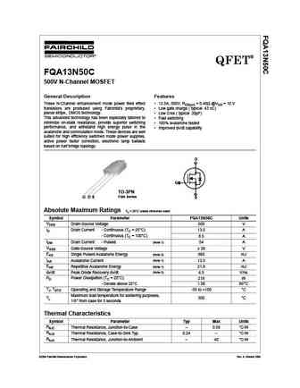
QFET FQA13N50C 500V N-Channel MOSFET General Description Features These N-Channel enhancement mode power field effect 13.5A, 500V, RDS(on) = 0.48 @VGS = 10 V transistors are produced using Fairchild s proprietary, Low gate charge ( typical 43 nC) planar stripe, DMOS technology. Low Crss ( typical 20pF) This advanced technology has been especially tailored to Fa
fqa13n50c f109.pdf
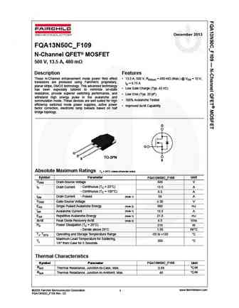
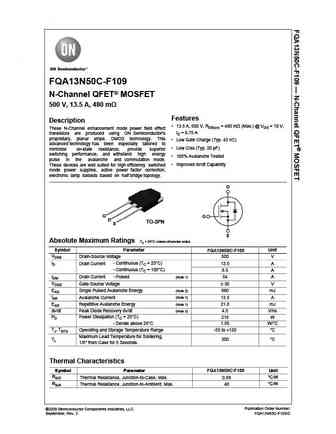
December 2013 FQA13N50C_F109 N-Channel QFET MOSFET 500 V, 13.5 A, 480 m Description Features These N-Channel enhancement mode power field effect 13.5 A, 500 V, RDS(on) = 480 m (Max.) @ VGS = 10 V, transistors are produced using Fairchild s proprietary, ID = 6.75 A planar stripe, DMOS technology. This advanced technology Low Gate Charge (Typ. 43 nC) has been especia
fqp13n50c fqpf13n50c.pdf
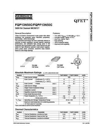
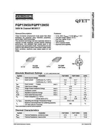
TM QFET FQP13N50C/FQPF13N50C 500V N-Channel MOSFET General Description Features These N-Channel enhancement mode power field effect 13A, 500V, RDS(on) = 0.48 @VGS = 10 V transistors are produced using Fairchild s proprietary, Low gate charge ( typical 43 nC) planar stripe, DMOS technology. Low Crss ( typical 20pF) This advanced technology has been especially tailored t
fqp13n50cf fqpf13n50cf.pdf
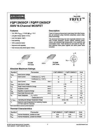
May 2006 TM FRFET FQP13N50CF / FQPF13N50CF 500V N-Channel MOSFET Features Description 13A, 500V, RDS(on) = 0.54 @VGS = 10 V These N-Channel enhancement mode power field effect transis- tors are produced using Fairchild s proprietary, planar stripe, Low gate charge (typical 43 nC) DMOS technology. Low Crss (typical 20pF) This advanced technology has been especially t
fdd3n50nztm.pdf
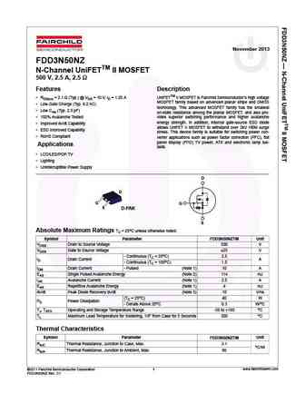
November 2013 FDD3N50NZ N-Channel UniFETTM II MOSFET 500 V, 2.5 A, 2.5 Features Description RDS(on) = 2.1 (Typ.) @ VGS = 10 V, ID = 1.25 A UniFETTM II MOSFET is Fairchild Semiconductor s high voltage MOSFET family based on advanced planar stripe and DMOS Low Gate Charge (Typ. 6.2 nC) technology. This advanced MOSFET family has the smallest Low Crss (Typ. 2.5 pF) on
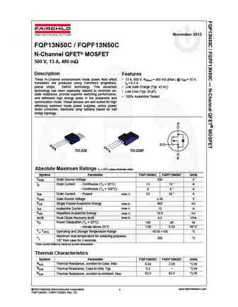
fqp13n50c fqpf13n50c.pdf
November 2013 FQP13N50C / FQPF13N50C N-Channel QFET MOSFET 500 V, 13 A, 480 m Description Features These N-Channel enhancement mode power field effect 13 A, 500 V, RDS(on) = 480 m (Max.) @ VGS = 10 V, transistors are produced using Fairchild s proprietary, ID = 6.5 A planar stripe, DMOS technology. This advanced Low Gate Charge (Typ. 43 nC) technology has been especia
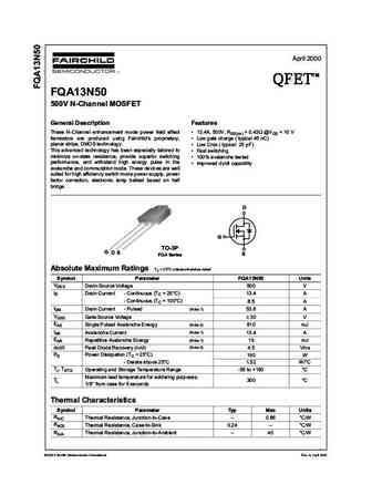
fqa13n50.pdf
April 2000 TM QFET QFET QFET QFET 500V N-ChanneI MOSFET GeneraI Description Features These N-Channel enhancement mode power field effect 13.4A, 500V, RDS(on) = 0.43 @VGS = 10 V transistors are produced using Fairchild s proprietary, Low gate charge ( typical 45 nC) planar stripe, DMOS technology. Low Crss ( typical 25 pF) This advanced technology has been
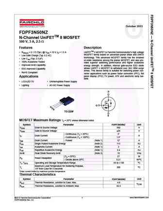
fdpf3n50nz.pdf
October 2013 FDPF3N50NZ N-Channel UniFETTM II MOSFET 500 V, 3 A, 2.5 Features Description RDS(on) = 2.1 (Typ.) @ VGS = 10 V, ID = 1.5 A UniFETTM II MOSFET is Fairchild Semiconductor s high voltage MOSFET family based on advanced planar stripe and DMOS Low Gate Charge (Typ. 6.2 nC) technology. This advanced MOSFET family has the smallest Low Crss (Typ. 2.5 pF
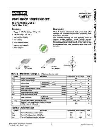
fdp13n50f fdpf13n50ft.pdf
September 2007 UniFETTM FDP13N50F / FDPF13N50FT tm N-Channel MOSFET 500V, 12A, 0.54 Features Description RDS(on) = 0.42 ( Typ.)@ VGS = 10V, ID = 6A These N-Channel enhancement mode power field effect transistors are produced using Fairchild s proprietary, planar Low gate charge ( Typ. 30nC) stripe, DMOS technology. Low Crss ( Typ. 14.5pF) This advanced technol
fqpf13n50 fqpf13n50t.pdf
TM QFET FQP13N50/FQPF13N50 500V N-Channel MOSFET General Description Features These N-Channel enhancement mode power field effect 12.5A, 500V, RDS(on) = 0.43 @VGS = 10 V transistors are produced using Fairchild s proprietary, Low gate charge ( typical 45 nC) planar stripe, DMOS technology. Low Crss ( typical 25 pF) This advanced technology has been especially tailored
fqa13n50cf.pdf
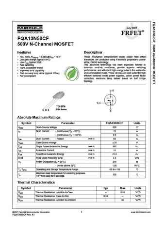
July 2007 FRFET FQA13N50CF 500V N-Channel MOSFET Features Description 15A, 500V, RDS(on) = 0.48 @VGS = 10 V These N-Channel enhancement mode power field effect Low gate charge (typical 43nC) transistors are produced using Fairchild s proprietary, planar stripe, DMOS technology. Low Crss (typical 20pF) This advanced technology has been especially tailored to
fdd3n50nz.pdf
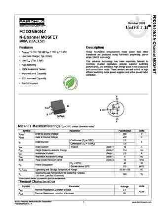
October 2009 UniFET-IITM FDD3N50NZ N-Channel MOSFET 500V, 2.5A, 2.5 Features Description RDS(on) = 2.1 ( Typ.)@ VGS = 10V, ID = 1.25A These N-Channel enhancement mode power field effect transistors are produced using Fairchild s proprietary, planar Low Gate Charge ( Typ. 6.2nC) stripe, DMOS technology. Low Crss ( Typ. 2.5pF) This advance technology has been esp
fqd3n50c fqu3n50c.pdf
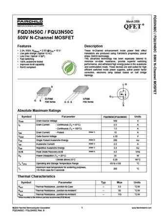
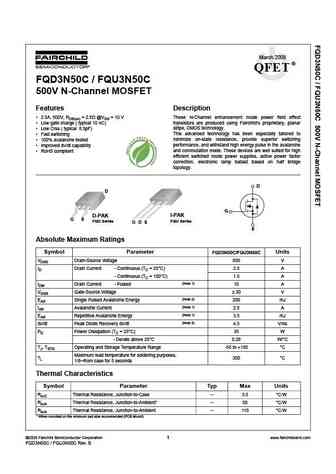
March 2008 QFET FQD3N50C / FQU3N50C 500V N-Channel MOSFET Features Description 2.5A, 500V, RDS(on) = 2.5 @VGS = 10 V These N-Channel enhancement mode power field effect Low gate charge ( typical 10 nC) transistors are produced using Fairchild s proprietary, planar stripe, DMOS technology. Low Crss ( typical 8.5pF) This advanced technology has been especially tai
fqp3n50c fqpf3n50c.pdf
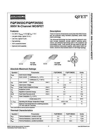
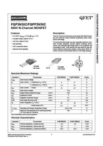
QFET FQP3N50C/FQPF3N50C 500V N-Channel MOSFET Features Description 3 A, 500 V, RDS(on) = 2.5 @ VGS = 10 V These N-Channel enhancement mode power field effect transis- tors are produced using Fairchild s proprietary, planar stripe, Low gate charge ( typical 10 nC ) DMOS technology. Low Crss ( typical 8.5 pF) This advanced technology has been especially tailored to
fqp13n50 fqpf13n50.pdf
TM QFET FQP13N50/FQPF13N50 500V N-Channel MOSFET General Description Features These N-Channel enhancement mode power field effect 12.5A, 500V, RDS(on) = 0.43 @VGS = 10 V transistors are produced using Fairchild s proprietary, Low gate charge ( typical 45 nC) planar stripe, DMOS technology. Low Crss ( typical 25 pF) This advanced technology has been especially tailored
fqp3n50c fqpf3n50c.pdf
QFET FQP3N50C/FQPF3N50C 500V N-Channel MOSFET Features Description 3 A, 500 V, RDS(on) = 2.5 @ VGS = 10 V These N-Channel enhancement mode power field effect transis- tors are produced using Fairchild s proprietary, planar stripe, Low gate charge ( typical 10 nC ) DMOS technology. Low Crss ( typical 8.5 pF) This advanced technology has been especially tailored to
fqpf13n50csdtu fqpf13n50ct.pdf
TM QFET FQP13N50C/FQPF13N50C 500V N-Channel MOSFET General Description Features These N-Channel enhancement mode power field effect 13A, 500V, RDS(on) = 0.48 @VGS = 10 V transistors are produced using Fairchild s proprietary, Low gate charge ( typical 43 nC) planar stripe, DMOS technology. Low Crss ( typical 20pF) This advanced technology has been especially tailored t
fqd3n50ctf.pdf
March 2008 QFET FQD3N50C / FQU3N50C 500V N-Channel MOSFET Features Description 2.5A, 500V, RDS(on) = 2.5 @VGS = 10 V These N-Channel enhancement mode power field effect Low gate charge ( typical 10 nC) transistors are produced using Fairchild s proprietary, planar stripe, DMOS technology. Low Crss ( typical 8.5pF) This advanced technology has been especially tai
rdd023n50.pdf
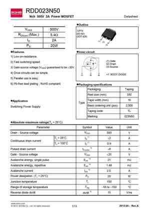
RDD023N50 Nch 500V 2A Power MOSFET Datasheet lOutline VDSS 500V CPT3 (SC-63) RDS(on) (Max.) 5.4W (SOT-428) ID 2A (1) (2) (3) PD 20W lFeatures lInner circuit 1) Low on-resistance. (1) Gate 2) Fast switching speed. (2) Drain (3) Source 3) Gate-source voltage (VGSS) guaranteed to be 30V. 4) Drive circuits can be simple. *1 BODY DIODE 5) Parallel use is easy.
irfps43n50k irfps43n50kpbf sihfps43n50k.pdf
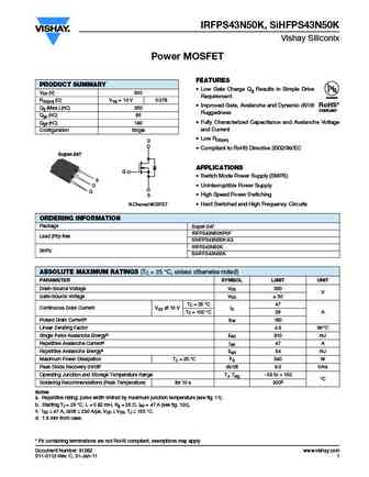
IRFPS43N50K, SiHFPS43N50K Vishay Siliconix Power MOSFET FEATURES PRODUCT SUMMARY Low Gate Charge Qg Results in Simple Drive VDS (V) 500 Requirement Available RDS(on) ( )VGS = 10 V 0.078 Improved Gate, Avalanche and Dynamic dV/dt RoHS* Qg (Max.) (nC) 350 COMPLIANT Ruggedness Qgs (nC) 85 Fully Characterized Capacitance and Avalanche Voltage Qgd (nC) 180 and Current
sihu3n50d.pdf
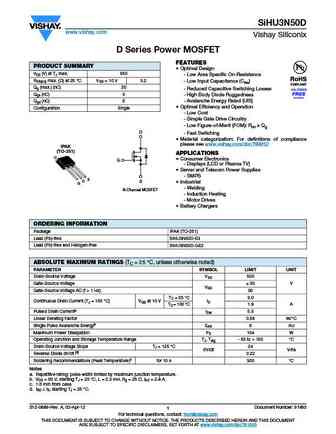
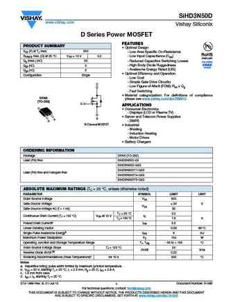
SiHU3N50D www.vishay.com Vishay Siliconix D Series Power MOSFET FEATURES PRODUCT SUMMARY Optimal Design VDS (V) at TJ max. 550 - Low Area Specific On-Resistance RDS(on) max. ( ) at 25 C VGS = 10 V 3.2 - Low Input Capacitance (Ciss) Qg (max.) (nC) 20 - Reduced Capacitive Switching Losses Qgs (nC) 3 - High Body Diode Ruggedness Qgd (nC) 5 - Avalanche Energy Rated (UIS)
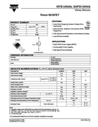
irfb13n50a sihfb13n50a.pdf
IRFB13N50A, SiHFB13N50A Vishay Siliconix Power MOSFET FEATURES PRODUCT SUMMARY Lower Gate Charge Qg Results in Simpler Drive VDS (V) 500 Reqirements Available RDS(on) ( )VGS = 10 V 0.450 RoHS* Improved Gate, Avalanche and Dynamic dV/dt Qg (Max.) (nC) 81 COMPLIANT Ruggedness Qgs (nC) 20 Qgd (nC) 36 Fully Characterized Capacitance and Avalanche Voltage Configuratio
sihu3n50da.pdf
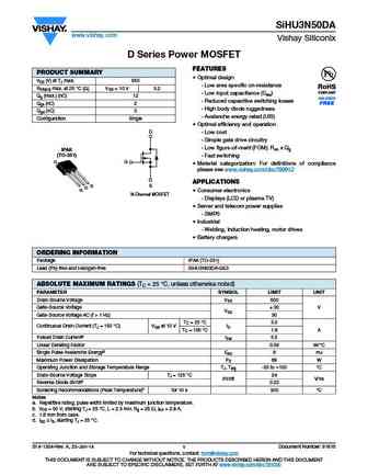
SiHU3N50DA www.vishay.com Vishay Siliconix D Series Power MOSFET FEATURES PRODUCT SUMMARY Optimal design VDS (V) at TJ max. 550 - Low area specific on-resistance RDS(on) max. at 25 C ( ) VGS = 10 V 3.2 - Low input capacitance (Ciss) Qg (max.) (nC) 12 - Reduced capacitive switching losses Qgs (nC) 2 - High body diode ruggedness Qgd (nC) 3 - Avalanche energy rated (UIS) Co
irfp23n50l sihfp23n50l.pdf
IRFP23N50L, SiHFP23N50L Vishay Siliconix Power MOSFET FEATURES PRODUCT SUMMARY Superfast Body Diode Eliminates the Need for VDS (V) 500 External Diodes in ZVS Applications Available RDS(on) ( )VGS = 10 V 0.190 Lower Gate Charge Results in Simpler Drive RoHS* Qg (Max.) (nC) 150 COMPLIANT Requirements Qgs (nC) 44 Enhanced dV/dt Capabilities Offer Improved Ruggedness
sihd3n50da.pdf
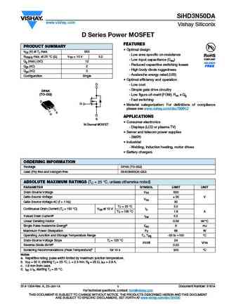
SiHD3N50DA www.vishay.com Vishay Siliconix D Series Power MOSFET FEATURES PRODUCT SUMMARY Optimal design VDS (V) at TJ max. 550 - Low area specific on-resistance RDS(on) max. at 25 C ( ) VGS = 10 V 3.2 - Low input capacitance (Ciss) Qg (max.) (nC) 12 - Reduced capacitive switching losses Qgs (nC) 2 - High body diode ruggedness Qgd (nC) 3 - Avalanche energy rated (UIS) Co
sihd3n50d.pdf
SiHD3N50D www.vishay.com Vishay Siliconix D Series Power MOSFET FEATURES PRODUCT SUMMARY Optimal Design VDS (V) at TJ max. 550 - Low Area Specific On-Resistance RDS(on) max. ( ) at 25 C VGS = 10 V 3.2 - Low Input Capacitance (Ciss) Qg (max.) (nC) 20 - Reduced Capacitive Switching Losses - High Body Diode Ruggedness Qgs (nC) 3 Available - Avalanche Energy Rated (UIS) Qgd
irfb13n50a irfb13n50apbf sihfb13n50a.pdf
IRFB13N50A, SiHFB13N50A Vishay Siliconix Power MOSFET FEATURES PRODUCT SUMMARY Lower Gate Charge Qg Results in Simpler Drive VDS (V) 500 Reqirements Available RDS(on) ( )VGS = 10 V 0.450 RoHS* Improved Gate, Avalanche and Dynamic dV/dt Qg (Max.) (nC) 81 COMPLIANT Ruggedness Qgs (nC) 20 Qgd (nC) 36 Fully Characterized Capacitance and Avalanche Voltage Configuratio
irfps43n50k sihfps43n50k.pdf
IRFPS43N50K, SiHFPS43N50K Vishay Siliconix Power MOSFET FEATURES PRODUCT SUMMARY Low Gate Charge Qg Results in Simple Drive VDS (V) 500 Requirement Available RDS(on) ( )VGS = 10 V 0.078 Improved Gate, Avalanche and Dynamic dV/dt RoHS* Qg (Max.) (nC) 350 COMPLIANT Ruggedness Qgs (nC) 85 Fully Characterized Capacitance and Avalanche Voltage Qgd (nC) 180 and Current
irfp23n50l irfp23n50lpbf sihfp23n50l.pdf
IRFP23N50L, SiHFP23N50L Vishay Siliconix Power MOSFET FEATURES PRODUCT SUMMARY Superfast Body Diode Eliminates the Need for VDS (V) 500 External Diodes in ZVS Applications Available RDS(on) ( )VGS = 10 V 0.190 Lower Gate Charge Results in Simpler Drive RoHS* Qg (Max.) (nC) 150 COMPLIANT Requirements Qgs (nC) 44 Enhanced dV/dt Capabilities Offer Improved Ruggedness
zxt13n50de6.pdf
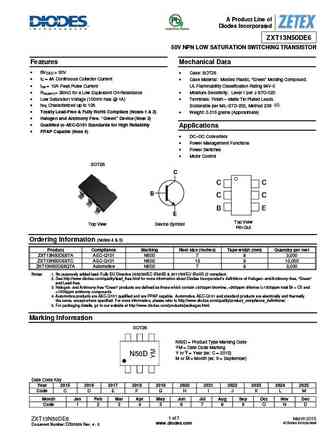
A Product Line of Diodes Incorporated ZXT13N50DE6 50V NPN LOW SATURATION SWITCHING TRANSISTOR Features Mechanical Data BVCEO > 50V Case SOT26 IC = 4A Continuous Collector Current Case Material Molded Plastic, Green Molding Compound. ICM = 10A Peak Pulse Current UL Flammability Classification Rating 94V-0 RCE(SAT) = 36m for a Low Equivalent On-Res
irfb13n50a sihfb13n50a.pdf
IRFB13N50A, SiHFB13N50A Vishay Siliconix Power MOSFET FEATURES PRODUCT SUMMARY Lower Gate Charge Qg Results in Simpler Drive VDS (V) 500 Available Reqirements RDS(on) ( )VGS = 10 V 0.450 RoHS* Qg (Max.) (nC) 81 Improved Gate, Avalanche and Dynamic dV/dt COMPLIANT Qgs (nC) 20 Ruggedness Qgd (nC) 36 Fully Characterized Capacitance and Avalanche Voltage Configuration
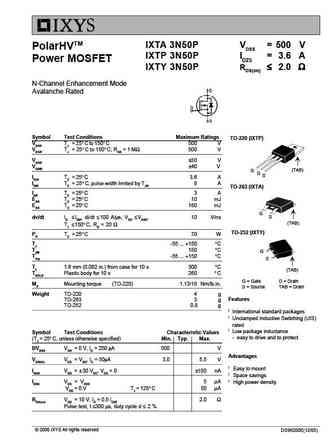
ixta3n50p ixtp3n50p ixty3n50p.pdf
IXTA 3N50P VDSS = 500 V PolarHVTM IXTP 3N50P ID25 = 3.6 A Power MOSFET IXTY 3N50P RDS(on) 2.0 N-Channel Enhancement Mode Avalanche Rated Symbol Test Conditions Maximum Ratings TO-220 (IXTP) VDSS TJ = 25 C to 150 C 500 V VDGR TJ = 25 C to 150 C; RGS = 1 M 500 V VGSS 30 V VGSM 40 V (TAB) G D S ID25 TC = 25 C 3.6 A IDM
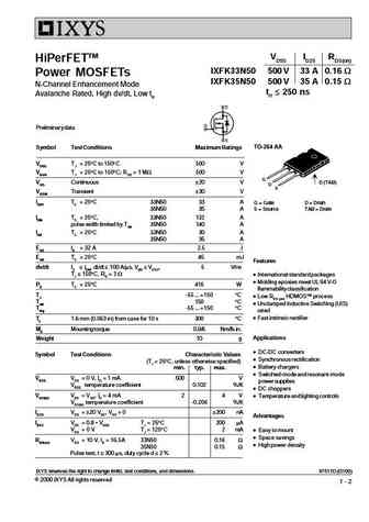
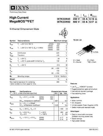
ixfk33n50 ixfk35n50.pdf
VDSS ID25 RDS(on) HiPerFETTM IXFK33N50 500 V 33 A 0.16 W Power MOSFETs IXFK35N50 500 V 35 A 0.15 W N-Channel Enhancement Mode trr 250 ns Avalanche Rated, High dv/dt, Low trr Preliminary data TO-264 AA Symbol Test Conditions Maximum Ratings VDSS TJ = 25 C to 150 C 500 V VDGR TJ = 25 C to 150 C; RGS = 1 MW 500 V G VGS Continuous 20 V D (TAB) D S VGSM Transient 30 V ID
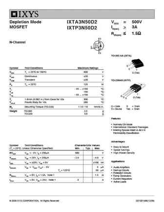
ixta3n50d2-ixtp3n50d2.pdf
Depletion Mode VDSX = 500V IXTA3N50D2 MOSFET ID(on) > 3A IXTP3N50D2 RDS(on) 1.5 N-Channel TO-263 AA (IXTA) G Symbol Test Conditions Maximum Ratings S VDSX TJ = 25 C to 150 C 500 V D (Tab) VGSX Continuous 20 V VGSM Transient 30 V TO-220AB (IXTP) PD TC = 25 C 125 W TJ - 55 ... +150 C TJM 150 C Tstg - 55 ... +150 C G D D (Tab)
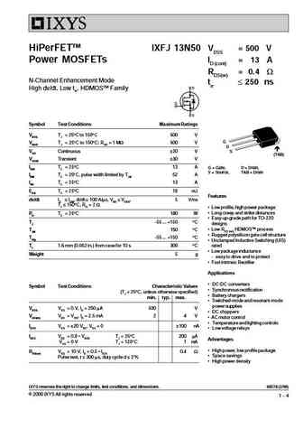
ixfj13n50.pdf
HiPerFETTM IXFJ 13N50 VDSS = 500 V Power MOSFETs ID (cont) = 13 A RDS(on) = 0.4 W N-Channel Enhancement Mode trr 250 ns High dv/dt, Low trr, HDMOSTM Family Symbol Test Conditions Maximum Ratings VDSS TJ = 25 C to 150 C 500 V G VDGR TJ = 25 C to 150 C; RGS = 1 MW 500 V D VGS Continuous 20 V S (TAB) VGSM Transient 30 V ID25 TC = 25 C13 A G = Gate, D = Drain, S = So
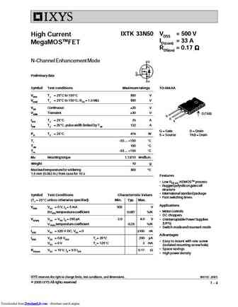
ixtk33n50.pdf
IXTK 33N50 VDSS = 500 V High Current ID (cont) = 33 A MegaMOSTMFET RDS(on) = 0.17 N-Channel Enhancement Mode Preliminary data Symbol Test conditions Maximum ratings TO-264 AA VDSS TJ = 25 C to 150 C 500 V VDGR TJ = 25 C to 150 C; RGS = 1.0 M 500 V VGS Continuous 20 V VGSM Transient 30 V D (TAB) G D ID25 TC = 25 C 33 A S IDM TC = 25 C, pulse
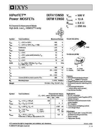
ixfh13n50 ixfm13n50.pdf
HiPerFETTM IXFH 13 N50 VDSS = 500 V Power MOSFETs IXFM 13 N50 ID (cont) = 13 A RDS(on) = 0.4 W N-Channel Enhancement Mode trr 250 ns High dv/dt, Low trr, HDMOSTM Family Symbol Test Conditions Maximum Ratings TO-247 AD (IXFH) VDSS TJ = 25 C to 150 C 500 V VDGR TJ = 25 C to 150 C; RGS = 1 MW 500 V (TAB) VGS Continuous 20 V VGSM Transient 30 V ID25 TC = 25 C13 A TO-204 AA
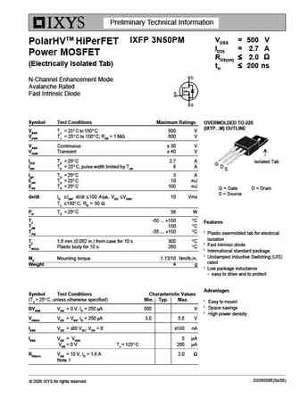
ixfp3n50pm.pdf
Preliminary Technical Information VDSS = 500 V IXFP 3N50PM PolarHVTM HiPerFET ID25 = 2.7 A Power MOSFET RDS(on) 2.0 (Electrically Isolated Tab) trr 200 ns N-Channel Enhancement Mode Avalanche Rated Fast Intrinsic Diode Symbol Test Conditions Maximum Ratings OVERMOLDED TO-220 (IXTP...M) OUTLINE VDSS TJ = 25 C t
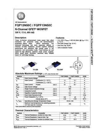
fqp13n50c fqpf13n50c.pdf
FQP13N50C / FQPF13N50C N-Channel QFET MOSFET 500 V, 13 A, 480 m Description Features These N-Channel enhancement mode power field effect 13 A, 500 V, RDS(on) = 480 m (Max.) @ VGS = 10 V, transistors are produced using ON Semiconductor s ID = 6.5 A proprietary, planar stripe, DMOS technology. This Low Gate Charge (Typ. 43 nC) advanced technology has been especially tail
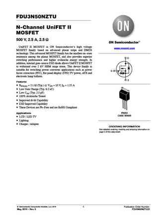
fdu3n50nztu.pdf
FDU3N50NZTU N-Channel UniFET II MOSFET 500 V, 2.5 A, 2.5 W UniFET II MOSFET is ON Semiconductor s high voltage www.onsemi.com MOSFET family based on advanced planar stripe and DMOS technology. This advanced MOSFET family has the smallest on-state resistance among the planar MOSFET, and also provides superior D switching performance and higher avalanche energy strength. In addition,
fdpf3n50nz.pdf
Is Now Part of To learn more about ON Semiconductor, please visit our website at www.onsemi.com Please note As part of the Fairchild Semiconductor integration, some of the Fairchild orderable part numbers will need to change in order to meet ON Semiconductor s system requirements. Since the ON Semiconductor product management systems do not have the ability to manage part nomenclatur
fqa13n50cf.pdf
Is Now Part of To learn more about ON Semiconductor, please visit our website at www.onsemi.com Please note As part of the Fairchild Semiconductor integration, some of the Fairchild orderable part numbers will need to change in order to meet ON Semiconductor s system requirements. Since the ON Semiconductor product management systems do not have the ability to manage part nomenclatur
fdd3n50nz.pdf
Is Now Part of To learn more about ON Semiconductor, please visit our website at www.onsemi.com Please note As part of the Fairchild Semiconductor integration, some of the Fairchild orderable part numbers will need to change in order to meet ON Semiconductor s system requirements. Since the ON Semiconductor product management systems do not have the ability to manage part nomenclatur
fqi13n50c.pdf
Is Now Part of To learn more about ON Semiconductor, please visit our website at www.onsemi.com Please note As part of the Fairchild Semiconductor integration, some of the Fairchild orderable part numbers will need to change in order to meet ON Semiconductor s system requirements. Since the ON Semiconductor product management systems do not have the ability to manage part nomenclatur
fqpf13n50cf.pdf
Is Now Part of To learn more about ON Semiconductor, please visit our website at www.onsemi.com Please note As part of the Fairchild Semiconductor integration, some of the Fairchild orderable part numbers will need to change in order to meet ON Semiconductor s system requirements. Since the ON Semiconductor product management systems do not have the ability to manage part nomenclatur
fqp13n50 fqpf13n50.pdf
TM QFET FQP13N50/FQPF13N50 500V N-Channel MOSFET General Description Features These N-Channel enhancement mode power field effect 12.5A, 500V, RDS(on) = 0.43 @VGS = 10 V transistors are produced using Fairchild s proprietary, Low gate charge ( typical 45 nC) planar stripe, DMOS technology. Low Crss ( typical 25 pF) This advanced technology has been especially tailored
fqa13n50c-f109.pdf
ON Semiconductor and are trademarks of Semiconductor Components Industries, LLC dba ON Semiconductor or its subsidiaries in the United States and/or other countries. ON Semiconductor owns the rights to a number of patents, trademarks, copyrights, trade secrets, and other intellectual property. A listing of ON Semiconductor s product/patent coverage may be accessed at www.onsemi.com/s
ndd03n50z.pdf
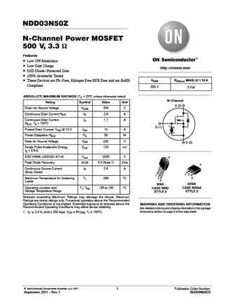
NDD03N50Z N-Channel Power MOSFET 500 V, 3.3 W Features Low ON Resistance Low Gate Charge http //onsemi.com ESD Diode-Protected Gate 100% Avalanche Tested VDSS RDS(on) (MAX) @ 1.15 A These Devices are Pb-Free, Halogen Free/BFR Free and are RoHS Compliant 500 V 3.3 W ABSOLUTE MAXIMUM RATINGS (TC = 25 C unless otherwise noted) N-Channel Rating Symbol Value Unit
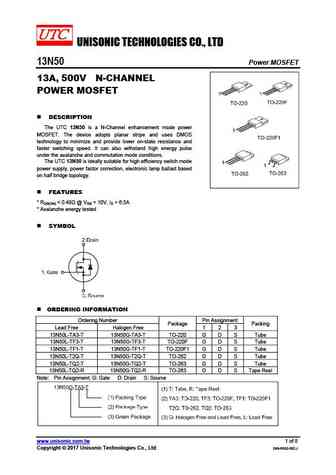
13n50l-ta3-t 13n50g-ta3-t 13n50l-tf3-t 13n50g-tf3-t 13n50l-tf1-t 13n50g-tf1-t.pdf
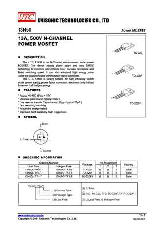
UNISONIC TECHNOLOGIES CO., LTD 13N50 Power MOSFET 13A, 500V N-CHANNEL POWER MOSFET DESCRIPTION The UTC 13N50 is a N-Channel enhancement mode power MOSFET. The device adopts planar stripe and uses DMOS technology to minimize and provide lower on-state resistance and faster switching speed. It can also withstand high energy pulse under the avalanche and commutation mode cond
13n50.pdf
UNISONIC TECHNOLOGIES CO., LTD 13N50 Power MOSFET 13A, 500V N-CHANNEL POWER MOSFET 1 TO-220 DESCRIPTION The UTC 13N50 is an N-Channel enhancement mode power MOSFET. The device adopts planar stripe and uses DMOS technology to minimize and provide lower on-state resistance and faster switching speed. It can also withstand high energy pulse 1 under the avalanche and commutat
13n50l-t2q-t 13n50g-t2q-t 13n50l-tq2-t 13n50g-tq2-t 13n50l-tq2-r 13n50g-tq2-r.pdf
UNISONIC TECHNOLOGIES CO., LTD 13N50 Power MOSFET 13A, 500V N-CHANNEL POWER MOSFET DESCRIPTION The UTC 13N50 is a N-Channel enhancement mode power MOSFET. The device adopts planar stripe and uses DMOS technology to minimize and provide lower on-state resistance and faster switching speed. It can also withstand high energy pulse under the avalanche and commutation mode cond
3n50z.pdf
UNISONIC TECHNOLOGIES CO., LTD 3N50Z Preliminary Power MOSFET 3A, 500V N-CHANNEL POWER MOSFET DESCRIPTION 1 TO-220F The UTC 3N50Z is an N-channel mode power MOSFET using UTC s advanced technology to provide customers with planar stripe and DMOS technology. This technology allows a minimum on-state resistance and superior switching performance. It also can withstand high e
fmv23n50es.pdf
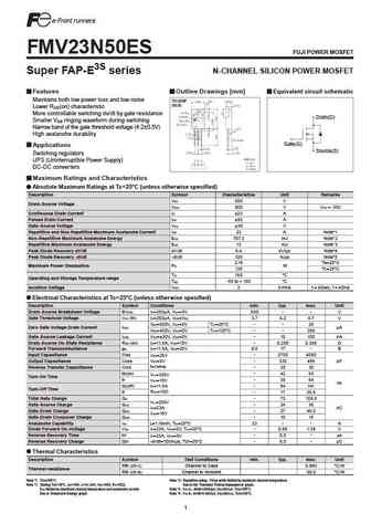
FMV23N50ES FUJI POWER MOSFET Super FAP-E3S series N-CHANNEL SILICON POWER MOSFET Features Outline Drawings [mm] Equivalent circuit schematic Maintains both low power loss and low noise TO-220F (SLS) Lower R (on) characteristic DS More controllable switching dv/dt by gate resistance Drain(D) Smaller V ringing waveform during switching GS Narrow band of the gate threshold voltage (4.2
fmv23n50e.pdf
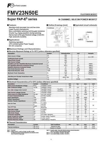
FMV23N50E FUJI POWER MOSFET Super FAP-E3 series N-CHANNEL SILICON POWER MOSFET Features Outline Drawings [mm] Equivalent circuit schematic Maintains both low power loss and low noise TO-220F(SLS) Lower R (on) characteristic DS More controllable switching dv/dt by gate resistance Drain(D) Smaller V ringing waveform during switching GS Narrow band of the gate threshold voltage (3.0 0.
fmh23n50es.pdf
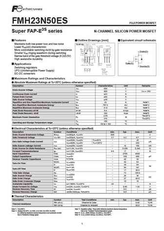
FMH23N50ES FUJI POWER MOSFET Super FAP-E3S series N-CHANNEL SILICON POWER MOSFET Features Outline Drawings [mm] Equivalent circuit schematic Maintains both low power loss and low noise TO-3P (Q) Lower R (on) characteristic DS More controllable switching dv/dt by gate resistance Drain(D) Smaller V ringing waveform during switching GS Narrow band of the gate threshold voltage (4.2 0.5
fmr23n50e.pdf
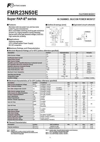
FMR23N50E FUJI POWER MOSFET Super FAP-E3 series N-CHANNEL SILICON POWER MOSFET Features Outline Drawings [mm] Equivalent circuit schematic Maintains both low power loss and low noise TO-3PF Lower R (on) characteristic DS More controllable switching dv/dt by gate resistance Drain(D) Smaller V ringing waveform during switching GS Narrow band of the gate threshold voltage (3.0 0.5V) H
fmr23n50es.pdf
FMR23N50ES FUJI POWER MOSFET Super FAP-E3S series N-CHANNEL SILICON POWER MOSFET Features Outline Drawings [mm] Equivalent circuit schematic Maintains both low power loss and low noise TO-3PF Lower R (on) characteristic DS More controllable switching dv/dt by gate resistance Drain(D) Smaller V ringing waveform during switching GS Narrow band of the gate threshold voltage (4.2 0.5V)
fmh23n50e.pdf
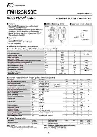
FMH23N50E FUJI POWER MOSFET Super FAP-E3 series N-CHANNEL SILICON POWER MOSFET Features Outline Drawings [mm] Equivalent circuit schematic Maintains both low power loss and low noise TO-3P(Q) Lower R (on) characteristic DS More controllable switching dv/dt by gate resistance Drain(D) Smaller V ringing waveform during switching GS Narrow band of the gate threshold voltage (3.0 0.5V)
tsm23n50cn.pdf
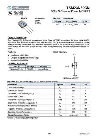
TSM23N50CN 500V N-Channel Power MOSFET TO-3PN Pin Definition PRODUCT SUMMARY 1. Gate VDS (V) RDS(on)(m ) ID (A) 2. Drain 3. Source 500 0.22 @ VGS =10V 23 General Description The TSM23N50CN N-Channel enhancement mode Power MOSFET is produced by planar stripe DMOS technology. This advanced technology has been especially tailored to minimize on-state resistance, provide
tsm13n50ci tsm13n50cz.pdf
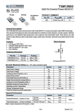
TSM13N50 500V N-Channel Power MOSFET TO-220 ITO-220 PRODUCT SUMMARY Pin Definition 1. Gate VDS (V) RDS(on)( ) ID (A) 2. Drain 3. Source 500 0.48 @ VGS =10V 13 General Description The TSM13N50 N-Channel enhancement mode Power MOSFET is produced by planar stripe DMOS technology. This advanced technology has been especially tailored to minimize on-state resistance, prov
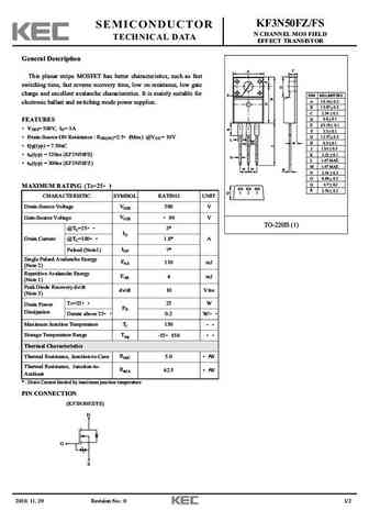
kf3n50fz-fs.pdf
KF3N50FZ/FS SEMICONDUCTOR N CHANNEL MOS FIELD TECHNICAL DATA EFFECT TRANSISTOR General Description C A This planar stripe MOSFET has better characteristics, such as fast switching time, fast reverse recovery time, low on resistance, low gate charge and excellent avalanche characteristics. It is mainly suitable for E DIM MILLIMETERS _ A 10.16 0.2 + electronic ballast and switchin
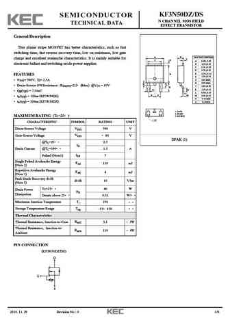
kf3n50dz-ds.pdf
KF3N50DZ/DS SEMICONDUCTOR N CHANNEL MOS FIELD TECHNICAL DATA EFFECT TRANSISTOR General Description This planar stripe MOSFET has better characteristics, such as fast switching time, fast reverse recovery time, low on resistance, low gate A K DIM MILLIMETERS charge and excellent avalanche characteristics. It is mainly suitable for L C D _ A 6.60 + 0.20 _ electronic ballast and s
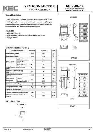
kf3n50dz-iz.pdf
KF3N50DZ/IZ SEMICONDUCTOR N CHANNEL MOS FIELD TECHNICAL DATA EFFECT TRANSISTOR General Description KF3N50DZ This planar stripe MOSFET has better characteristics, such as fast switching time, fast reverse recovery time, low on resistance, low gate A K DIM MILLIMETERS charge and excellent avalanche characteristics. It is mainly suitable for L C D _ A 6.60 + 0.20 _ electronic bal
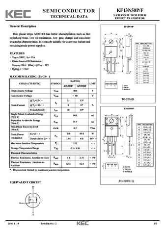
kf13n50p-f.pdf
KF13N50P/F SEMICONDUCTOR N CHANNEL MOS FIELD TECHNICAL DATA EFFECT TRANSISTOR General Description KF13N50P This planar stripe MOSFET has better characteristics, such as fast switching time, low on resistance, low gate charge and excellent avalanche characteristics. It is mainly suitable for electronic ballast and switching mode power supplies. FEATURES VDSS= 500V, ID= 13A Dra
aot13n50 aotf13n50.pdf
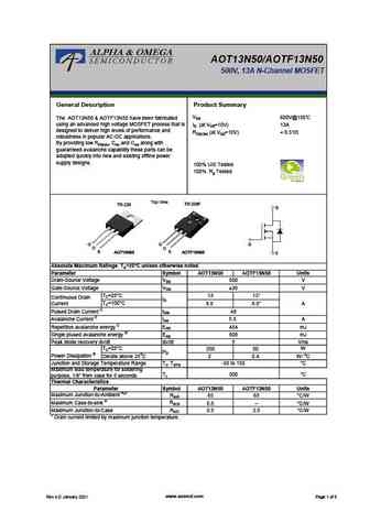
AOT13N50/AOTF13N50 500V, 13A N-Channel MOSFET General Description Product Summary VDS 600V@150 The AOT13N50 & AOTF13N50 have been fabricated using an advanced high voltage MOSFET process that is ID (at VGS=10V) 13A designed to deliver high levels of performance and RDS(ON) (at VGS=10V)
aotf3n50.pdf
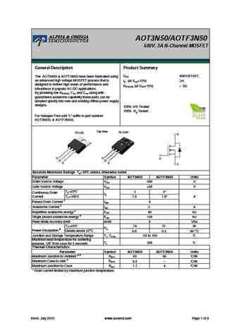
AOT3N50/AOTF3N50 500V, 3A N-Channel MOSFET General Description Product Summary VDS 600V@150 The AOT3N50 & AOTF3N50 have been fabricated using an advanced high voltage MOSFET process that is ID (at VGS=10V) 3A designed to deliver high levels of performance and RDS(ON) (at VGS=10V)
aod3n50.pdf
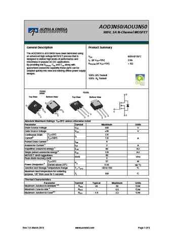
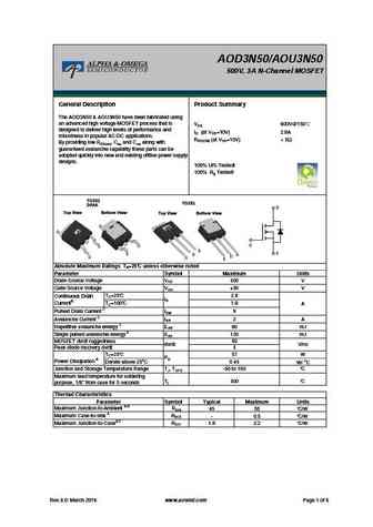
AOD3N50/AOU3N50 500V, 3A N-Channel MOSFET General Description Product Summary The AOD3N50 & AOU3N50 have been fabricated using an advanced high voltage MOSFET process that is VDS 600V@150 designed to deliver high levels of performance and ID (at VGS=10V) 2.8A robustness in popular AC-DC applications. RDS(ON) (at VGS=10V)
aot13n50.pdf
AOT13N50/AOTF13N50 500V, 13A N-Channel MOSFET General Description Product Summary VDS 600V@150 The AOT13N50 & AOTF13N50 have been fabricated using an advanced high voltage MOSFET process that is ID (at VGS=10V) 13A designed to deliver high levels of performance and RDS(ON) (at VGS=10V)
aou3n50.pdf
AOD3N50/AOU3N50 500V, 3A N-Channel MOSFET General Description Product Summary The AOD3N50 & AOU3N50 have been fabricated using an advanced high voltage MOSFET process that is VDS 600V@150 designed to deliver high levels of performance and ID (at VGS=10V) 2.8A robustness in popular AC-DC applications. RDS(ON) (at VGS=10V)
aod3n50 aou3n50.pdf
AOD3N50/AOU3N50 500V, 3A N-Channel MOSFET General Description Product Summary The AOD3N50 & AOU3N50 have been fabricated using an advanced high voltage MOSFET process that is VDS 600V@150 designed to deliver high levels of performance and ID (at VGS=10V) 2.8A robustness in popular AC-DC applications. RDS(ON) (at VGS=10V)
aotf13n50.pdf
AOT13N50/AOTF13N50 500V, 13A N-Channel MOSFET General Description Product Summary VDS 600V@150 The AOT13N50 & AOTF13N50 have been fabricated using an advanced high voltage MOSFET process that is ID (at VGS=10V) 13A designed to deliver high levels of performance and RDS(ON) (at VGS=10V)
aot3n50.pdf
AOT3N50/AOTF3N50 500V, 3A N-Channel MOSFET General Description Product Summary VDS 600V@150 The AOT3N50 & AOTF3N50 have been fabricated using an advanced high voltage MOSFET process that is ID (at VGS=10V) 3A designed to deliver high levels of performance and RDS(ON) (at VGS=10V)
ap13n50r-hf.pdf
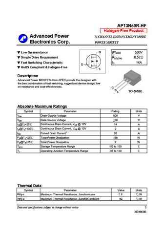
AP13N50R-HF Halogen-Free Product Advanced Power N-CHANNEL ENHANCEMENT MODE Electronics Corp. POWER MOSFET D Low On-resistance BVDSS 500V Simple Drive Requirement RDS(ON) 0.52 Fast Switching Characteristic ID 14A G RoHS Compliant & Halogen-Free S Description Advanced Power MOSFETs from APEC provide the designer with the best combination of fast switching, ruggedize
ap13n50w.pdf
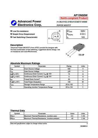
AP13N50W RoHS-compliant Product Advanced Power N-CHANNEL ENHANCEMENT MODE Electronics Corp. POWER MOSFET D Low On-resistance BVDSS 500V Simple Drive Requirement RDS(ON) 0.52 Fast Switching Characteristic ID 14A G S Description Advanced Power MOSFETs from APEC provide the designer with the best combination of fast switching, ruggedized device design, low on-resistance
ap13n50r.pdf
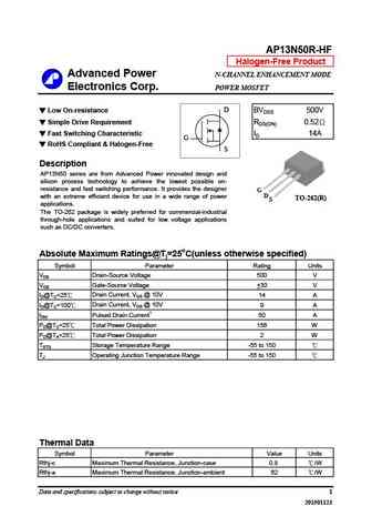
AP13N50R-HF Halogen-Free Product Advanced Power N-CHANNEL ENHANCEMENT MODE Electronics Corp. POWER MOSFET D Low On-resistance BVDSS 500V Simple Drive Requirement RDS(ON) 0.52 Fast Switching Characteristic ID 14A G RoHS Compliant & Halogen-Free S Description AP13N50 series are from Advanced Power innovated design and silicon process technology to achieve the lowest
ap13n50i-hf.pdf
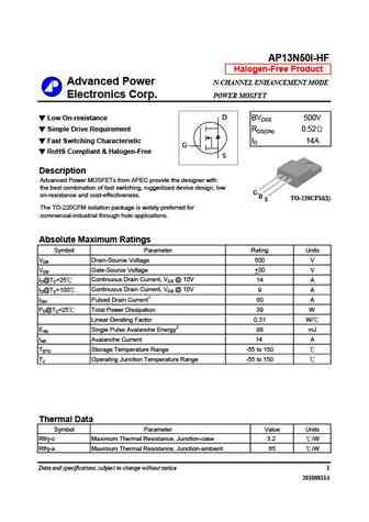
AP13N50I-HF Halogen-Free Product Advanced Power N-CHANNEL ENHANCEMENT MODE Electronics Corp. POWER MOSFET D Low On-resistance BVDSS 500V Simple Drive Requirement RDS(ON) 0.52 Fast Switching Characteristic ID 14A G RoHS Compliant & Halogen-Free S Description Advanced Power MOSFETs from APEC provide the designer with the best combination of fast switching, ruggedize
sif13n50c.pdf
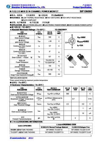
Shenzhen SI Semiconductors Co., LTD. Product Specification Shenzhen SI Semiconductors Co., LTD. Product Specification Shenzhen SI Semiconductors Co., LTD. Product Specification Shenzhen SI Semiconductors Co., LTD. Product Specification N- MOS / N-CHANNEL POWER MOSFET SIF13N50C N- MOS / N-CHANNEL POWER MOSFET SIF13N50C N- MOS / N-CHA
jcs13n50ft.pdf
N N- CHANNEL MOSFET R JCS13N50FT MAIN CHARACTERISTICS Package ID 13 A VDSS 500 V Rdson-max @Vgs=10V 0.46 Qg-typ 37 nC APPLICATIONS High frequency switching mode power supply UPS Electronic ballast UPS FEATUR
mtn13n50e3.pdf
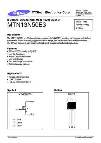
Spec. No. C405E3 Issued Date 2008.12.01 CYStech Electronics Corp. Revised Date 2009.08.13 Page No. 1/8 N-Channel Enhancement Mode Power MOSFET BVDSS 500V RDS(ON) 0.48 MTN13N50E3 ID 13A Description The MTN13N50E3 is a N-channel enhancement-mode MOSFET, providing the designer with the best combination of fast switching, ruggedized device design, low on-resis
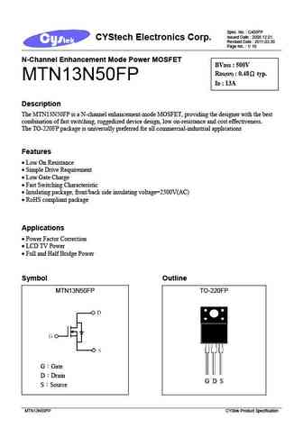
mtn13n50fp.pdf
Spec. No. C405FP Issued Date 2008.12.01 CYStech Electronics Corp. Revised Date 2011.03.30 Page No. 1/ 10 N-Channel Enhancement Mode Power MOSFET BVDSS 500V RDS(ON) 0.48 typ. MTN13N50FP ID 13A Description The MTN13N50FP is a N-channel enhancement-mode MOSFET, providing the designer with the best combination of fast switching, ruggedized device design, low o
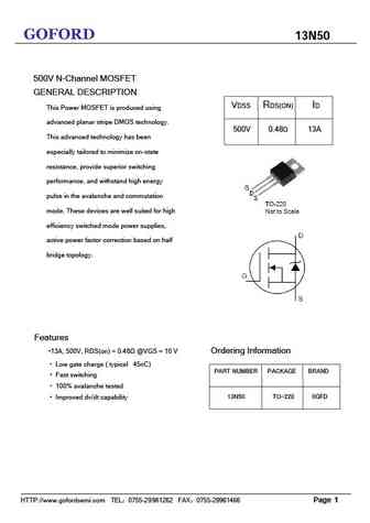
13n50.pdf
GOFORD 13N50 500V N-Channel MOSFET GENERAL DESCRIPTION VDSS RDS(ON) ID This Power MOSFET is produced using advanced planar stripe DMOS technology. 500V 0.48 13A This advanced technology has been especially tailored to minimize on-state resistance, provide superior switching performance, and withstand high energy pulse in the avalanche and commutation mode. These devices are well
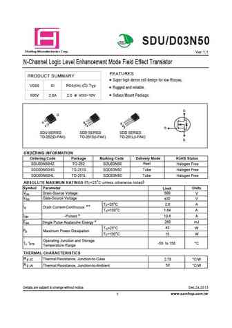
sdu03n50 sdd03n50.pdf
Green Product SDU/D03N50 a S mHop Microelectronics C orp. Ver 1.1 N-Channel Logic Level Enhancement Mode Field Effect Transistor FEATURES PRODUCT SUMMARY Super high dense cell design for low RDS(ON). VDSS ID RDS(ON) ( ) Typ Rugged and reliable. 500V 2.6A 2.0 @ VGS=10V Suface Mount Package. D G S SDU SERIES SDD SERIES SDD SERIES TO-252(D-PAK) TO-251S(I-PAK) TO-251L(I-PAK) ORDER
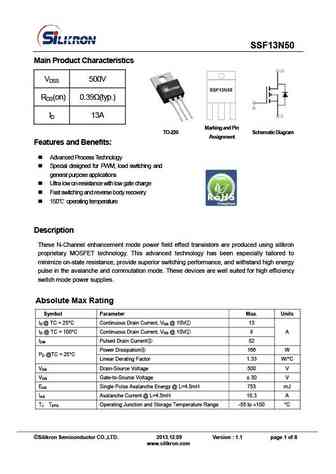
ssf13n50.pdf
SSF13N50 Main Product Characteristics VDSS 500V RDS(on) 0.39 (typ.) ID 13A Marking and Pin TO-220 Schematic Diagram Assignment Features and Benefits Advanced Process Technology Special designed for PWM, load switching and general purpose applications Ultra low on-resistance with low gate charge Fast switching and reverse body recovery 150 o
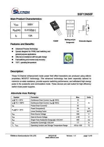
ssf13n50f.pdf
SSF13N50F Main Product Characteristics VDSS 500V RDS(on) 0.41 (typ.) ID 13A Marking a nd p in Sche ma ti c di agr a m TO220F Assignment Features and Benefits Advanced Process Technology Special designed for PWM, load switching and general purpose applications Ultra low on-resistance with low gate charge Fast switching and reverse body recovery
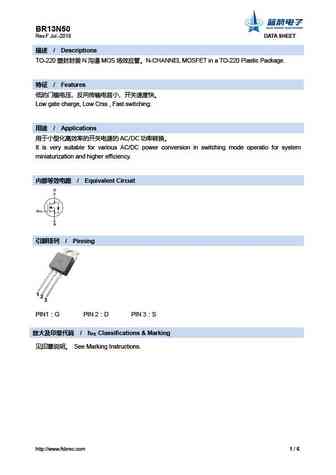
br13n50.pdf
BR13N50 Rev.F Jul.-2018 DATA SHEET / Descriptions TO-220 N MOS N-CHANNEL MOSFET in a TO-220 Plastic Package. / Features Low gate charge, Low Crss , Fast switching. / Applications AC/DC It is very suit
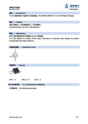
brb13n50.pdf
BRB13N50 Rev.A Nov.-2016 DATA SHEET / Descriptions TO-263 N MOS N-CHANNEL MOSFET in a TO-263Plastic Package. / Features Low gate charge, Low Crss , Fast switching. / Applications AC/DC It is very suit
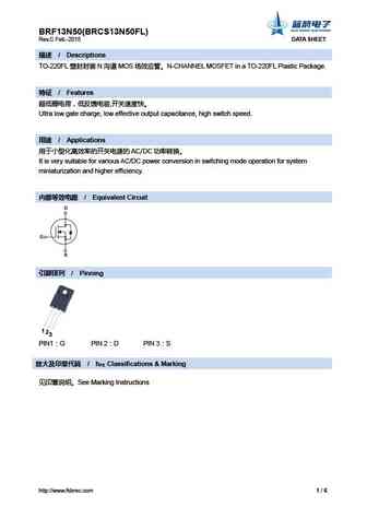
brf13n50.pdf
BRF13N50(BRCS13N50FL) Rev.C Feb.-2015 DATA SHEET / Descriptions TO-220FL N MOS N-CHANNEL MOSFET in a TO-220FL Plastic Package. / Features , Ultra low gate charge, low effective output capacitance, high switch speed. / Applications
brfl13n50.pdf
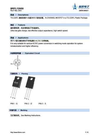
BRFL13N50 Rev.F Mar.-2023 DATA SHEET / Descriptions TO-220FL N MOS N-CHANNEL MOSFET in a TO-220FL Plastic Package. / Features , Ultra low gate charge, low effective output capacitance, high switch speed. / Applications AC/DC
irf13n50.pdf
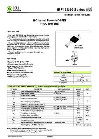
RoHS IRF13N50 Series RoHS SEMICONDUCTOR Nell High Power Products N-Channel Power MOSFET (14A, 500Volts) DESCRIPTION The Nell IRF13N50 are N-channel enhancement mode D silicon gate power field effect transistors. They are designed, tested and guaranteed to withstand level of energy in breakdown avalanche made of operation. They are designed as an extremely efficient and reliab
hfp13n50.pdf
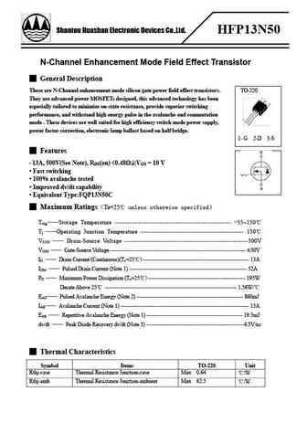
Shantou Huashan Electronic Devices Co.,Ltd. HFP13N50 N-Channel Enhancement Mode Field Effect Transistor General Description These are N-Channel enhancement mode silicon gate power field effect transistors. TO-220 They are advanced power MOSFETs designed, this advanced technology has been especially tailored to minimize on-state resistance, provide superior switching performan
cs13n50 a8d.pdf
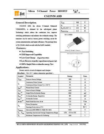
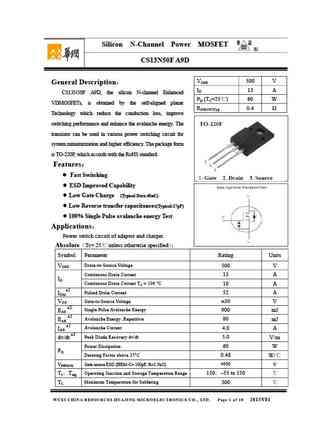
Silicon N-Channel Power MOSFET R CS13N50 A8D VDSS 500 V General Description ID 13 A CS13N50 A8D, the silicon N-channel Enhanced PD (TC=25 ) 125 W VDMOSFETs, is obtained by the self-aligned planar RDS(ON)Typ 0.4 Technology which reduce the conduction loss, improve switching performance and enhance the avalanche energy. The transistor can be used in various
cs13n50f a9d.pdf
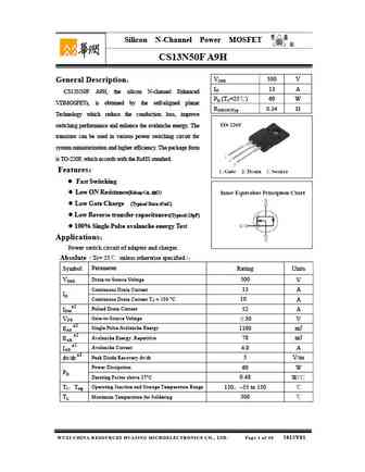
Silicon N-Channel Power MOSFET R CS13N50F A9D VDSS 500 V General Description ID 13 A CS13N50F A9D, the silicon N-channel Enhanced PD (TC=25 ) 60 W VDMOSFETs, is obtained by the self-aligned planar RDS(ON)Typ 0.4 Technology which reduce the conduction loss, improve switching performance and enhance the avalanche energy. The transistor can be used in various po
cs3n50 b4hy.pdf
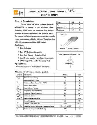
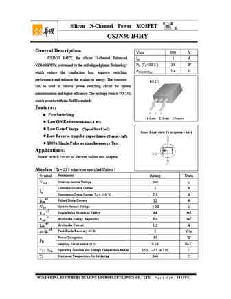
Silicon N-Channel Power MOSFET R CS3N50 B4HY General Description VDSS 500 V CS3N50 B4HY, the silicon N-channel Enhanced ID 3 A PD (TC=25 ) 35 W VDMOSFETs, is obtained by the self-aligned planar Technology RDS(ON)Typ 2.4 which reduce the conduction loss, improve switching performance and enhance the avalanche energy. The transistor can be used in various po
cs3n50 b4.pdf
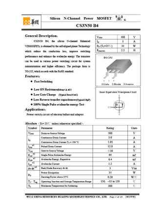
Silicon N-Channel Power MOSFET R CS3N50 B4 General Description VDSS 500 V CS3N50 B4, the silicon N-channel Enhanced ID 3 A PD (TC=25 ) 35 W VDMOSFETs, is obtained by the self-aligned planar Technology RDS(ON) 2.5 which reduce the conduction loss, improve switching performance and enhance the avalanche energy. The transistor can be used in various power swi
cs3n50 b3.pdf
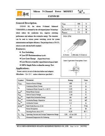
Silicon N-Channel Power MOSFET R CS3N50 B3 General Description VDSS 500 V CS3N50 B3, the silicon N-channel Enhanced ID 3 A PD (TC=25 ) 35 W VDMOSFETs, is obtained by the self-aligned planar Technology RDS(ON) 2.5 which reduce the conduction loss, improve switching performance and enhance the avalanche energy. The transistor can be used in various power swit
cs13n50 a8r.pdf
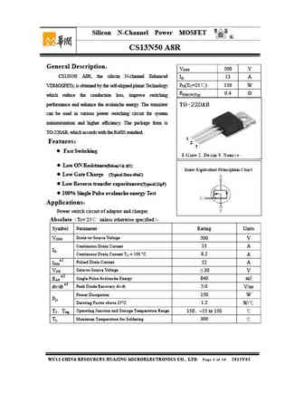
Silicon N-Channel Power MOSFET R CS13N50 A8R General Description VDSS 500 V CS13N50 A8R, the silicon N-channel Enhanced ID 13 A PD(TC=25 ) 150 W VDMOSFETs, is obtained by the self-aligned planar Technology RDS(ON)Typ 0.4 which reduce the conduction loss, improve switching performance and enhance the avalanche energy. The transistor can be used in various pow
cs13n50 a8h.pdf
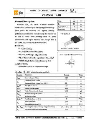
Silicon N-Channel Power MOSFET R CS13N50 A8H VDSS 500 V General Description ID 13 A CS13N50 A8H, the silicon N-channel Enhanced PD (TC=25 ) 150 W VDMOSFETs, is obtained by the self-aligned planar Technology RDS(ON)Typ 0.34 which reduce the conduction loss, improve switching performance and enhance the avalanche energy. The transistor can be used in various p
cs13n50f a9r.pdf
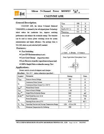
Silicon N-Channel Power MOSFET R CS13N50F A9R General Description VDSS 500 V CS13N50F A9R, the silicon N-channel Enhanced ID 13 A PD(TC=25 ) 42 W VDMOSFETs, is obtained by the self-aligned planar Technology RDS(ON)Typ 0.4 which reduce the conduction loss, improve switching performance and enhance the avalanche energy. The transistor can be used in various po
cs3n50 b3hy.pdf
Silicon N-Channel Power MOSFET R CS3N50 B3HY General Description VDSS 500 V CS3N50 B3HY, the silicon N-channel Enhanced ID 3 A VDMOSFETs, is obtained by the self-aligned planar PD (TC=25 ) 35 W RDS(ON)Typ 2.4 Technology which reduce the conduction loss, improve switching performance and enhance the avalanche energy. The transistor can be used in various powe
cs13n50f a9h.pdf
Silicon N-Channel Power MOSFET R CS13N50F A9H VDSS 500 V General Description ID 13 A CS13N50F A9H, the silicon N-channel Enhanced PD (TC=25 ) 60 W VDMOSFETs, is obtained by the self-aligned planar RDS(ON)Typ 0.34 Technology which reduce the conduction loss, improve switching performance and enhance the avalanche energy. The transistor can be used in variou
cm13n50.pdf
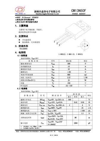
R C1N0 M35 www.jdsemi.cn ShenZhen Jingdao Electronic Co.,Ltd. POWER MOSFET 500V N-Channel VDMOS RoHS 1 2 3
e13n50.pdf
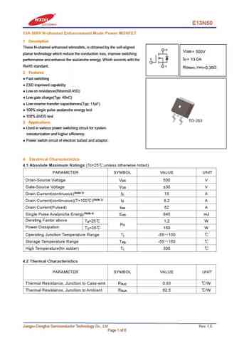
E13N50 13A 500V N-channel Enhancement Mode Power MOSFET 1 Description These N-channel enhanced vdmosfets, is obtained by the self-aligned V DSS = 500V planar technology which reduce the conduction loss, improve switching I = 13.0A D performance and enhance the avalanche energy. Which accords with the RoHS standard. R DS(on) TYP) =0.35 2 Features Fast switching ESD im
f13n50.pdf
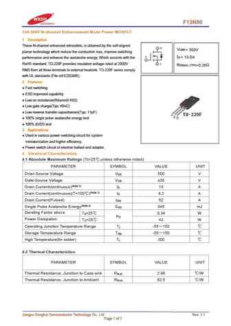
F13N50 13A 500V N-channel Enhancement Mode Power MOSFET 1 Description These N-channel enhanced vdmosfets, is obtained by the self-aligned V DSS = 500V planar technology which reduce the conduction loss, improve switching I = 13.0A D performance and enhance the avalanche energy. Which accords with the RoHS standard. TO-220F provides insulation voltage rated at 2000V R DS(on) TYP)
13n50.pdf
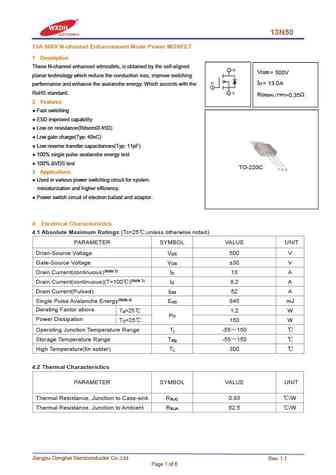
13N50 13A 500V N-channel Enhancement Mode Power MOSFET 1 Description These N-channel enhanced vdmosfets, is obtained by the self-aligned V DSS = 500V planar technology which reduce the conduction loss, improve switching I = 13.0A D performance and enhance the avalanche energy. Which accords with the RoHS standard. R DS(on) TYP) =0.35 2 Features Fast switching ESD imp
23n50d.pdf
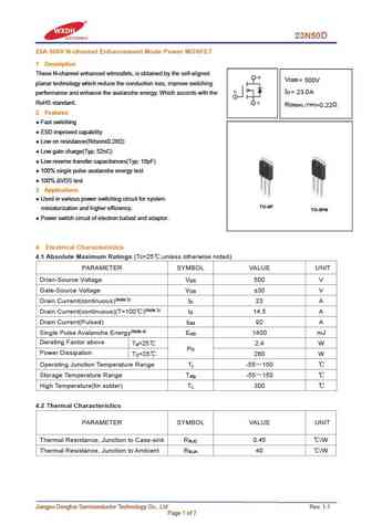
23N50D 23A 500V N-channel Enhancement Mode Power MOSFET 1 Description These N-channel enhanced vdmosfets, is obtained by the self-aligned V DSS = 500V planar technology which reduce the conduction loss, improve switching I = 23.0A D performance and enhance the avalanche energy. Which accords with the RoHS standard. R DS(on) TYP) =0.22 2 Features Fast switching ESD im
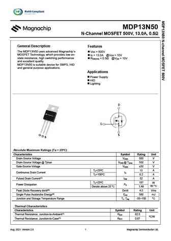
mdp13n50th.pdf
MDP13N50 N-Channel MOSFET 500V, 13.0A, 0.5 General Description Features The MDP13N50 uses advanced Magnachip s V = 500V DS MOSFET Technology, which provides low on- I = 13.0A @V = 10V D GS state resistance, high switching performance R
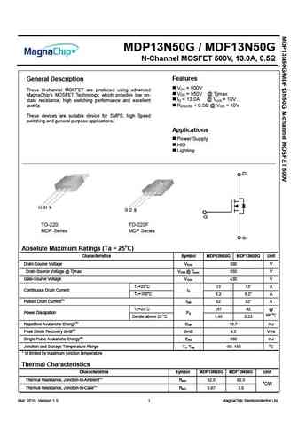
mdf13n50gth mdp13n50gth.pdf
MDP13N50G / MDF13N50G N-Channel MOSFET 500V, 13.0A, 0.5 General Description Features VDS = 500V These N-channel MOSFET are produced using advanced VDS = 550V @ Tjmax MagnaChip s MOSFET Technology, which provides low on- ID = 13.0A @ VGS = 10V state resistance, high switching performance and excellent RDS(ON)
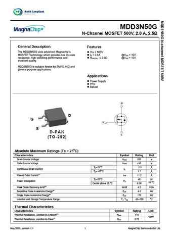
mdd3n50grh.pdf
MDD3N50G N-Channel MOSFET 500V, 2.8 A, 2.5 General Description Features The MDD3N50G uses advanced Magnachip s V = 500V DS MOSFET Technology, which provides low on-state @VGS = 10V ID = 2.8A resistance, high switching performance and @V = 10V R 2.5 DS(ON) GS excellent quality. MDD3N50G is suitable device for SMPS, HID and general purpose applications. App
mdq23n50dtp.pdf
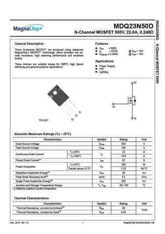
MDQ23N50D N-Channel MOSFET 500V, 23.0A, 0.245 General Description Features . VDS = 500V These N-channel MOSFET are produced using advanced ID = 23.0A @ VGS = 10V MagnaChip s MOSFET Technology, which provides low on- RDS(ON) 0.245 @ VGS = 10V state resistance, high switching performance and excellent quality. Applications These devices are suitable device fo
mdf13n50bth mdp13n50bth.pdf
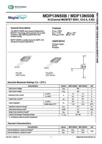
MDP13N50B / MDF13N50B N-Channel MOSFET 500V, 13.0 A, 0.5 General Description Features The MDP/F13N50B uses advanced Magnachip s VDS = 500V MOSFET Technology, which provides low on-state ID = 13.0A @VGS = 10V resistance, high switching performance and RDS(ON) 0.5 @VGS = 10V excellent quality. MDP/F13N50B is suitable device for SMPS, HID Applications and general p
msf13n50.pdf
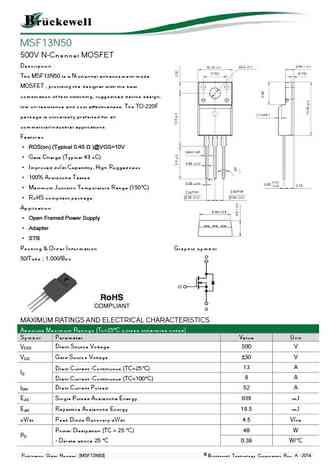
MSF13N50 500V N-Channel MOSFET Description The MSF13N50 is a N-channel enhancement-mode MOSFET , providing the designer with the best combination of fast switching, ruggedized device design, low on-resistance and cost effectiveness. The TO-220F package is universally preferred for all commercial-industrial applications Features RDS(on) (Typical 0.48 )@VGS=10V Ga
ms13n50.pdf
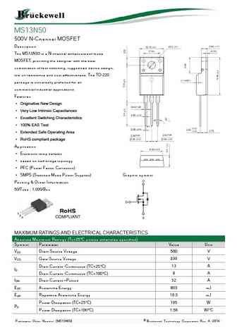
MS13N50 500V N-Channel MOSFET Description The MS13N50 is a N-channel enhancement-mode MOSFET, providing the designer with the best combination of fast switching, ruggedized device design, low on-resistance and cost effectiveness. The TO-220 package is universally preferred for all commercial-industrial applications Features Originative New Design Very Low Intrinsic
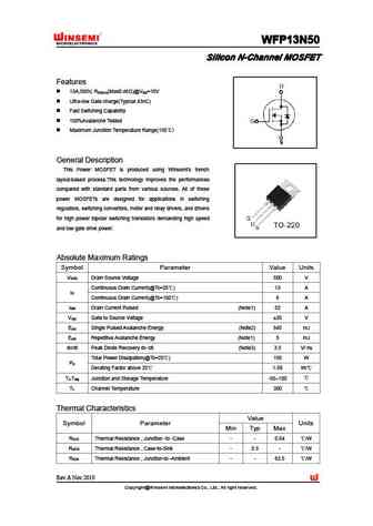
wfp13n50.pdf
WFP13N50 WFP13N50 WFP13N50 WFP13N50 Silicon N-Channel MOSFET Silicon N-Channel MOSFET Silicon N-Channel MOSFET Silicon N-Channel MOSFET Features 13A,500V, R (Max0.46 )@V =10V DS(on) GS Ultra-low Gate charge(Typical 43nC) Fast Switching Capability 100%Avalanche Tested Maximum Junction Temperature Range(150 ) General Description This Power MOSFET is produce
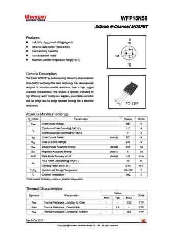
wff13n50.pdf
WFF13N50 WFF13N50 WFF13N50 WFF13N50 Silicon N-Channel MOSFET Silicon N-Channel MOSFET Silicon N-Channel MOSFET Silicon N-Channel MOSFET Features 13A,500V, R (Max0.46 )@V =10V DS(on) GS Ultra-low Gate charge(Typical 43nC) Fast Switching Capability 100%Avalanche Tested Maximum Junction Temperature Range(150 ) General Description This Power MOSFET is produce
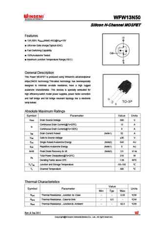
wfw13n50.pdf
WFW13N50 WFW13N50 WFW13N50 WFW13N50 Silicon N-Channel MOSFET Silicon N-Channel MOSFET Silicon N-Channel MOSFET Silicon N-Channel MOSFET Features 13A,500V, R (Max0.46 )@V =10V DS(on) GS Ultra-low Gate charge(Typical 43nC) Fast Switching Capability 100%Avalanche Tested Maximum Junction Temperature Range(150 ) General Description This Power MOSFET is produce
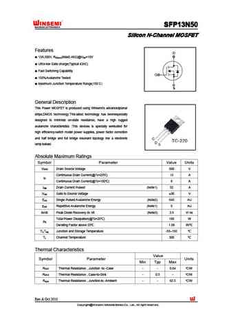
sfp13n50.pdf
SFP13N50 SFP13N50 SFP13N50 SFP13N50 Silicon N-Channel MOSFET Silicon N-Channel MOSFET Silicon N-Channel MOSFET Silicon N-Channel MOSFET Features 13A,500V, R (Max0.46 )@V =10V DS(on) GS Ultra-low Gate charge(Typical 43nC) Fast Switching Capability 100%Avalanche Tested Maximum Junction Temperature Range(150 ) General Description This Power MOSFET is produce
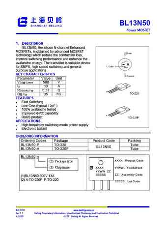
bl13n50-p bl13n50-a.pdf
BL13N50 Power MOSFET 1 Description BL13N50, the silicon N-channel Enhanced MOSFETs, is obtained by advanced MOSFET technology which reduce the conduction loss, improve switching performance and enhance the avalanche energy. The transistor is suitable device for SMPS, high speed switching and general purpose applications. KEY CHARACTERISTICS Parameter Value Unit V 500 V
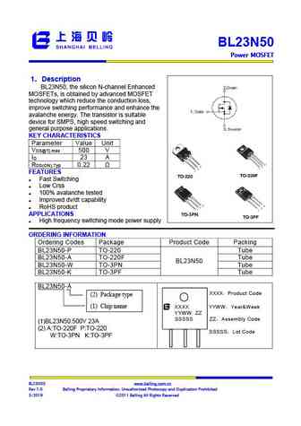
bl23n50-p bl23n50-a bl23n50-w bl23n50-k.pdf
BL23N50 Power MOSFET Power MOSFET Power MOSFET Power MOSFET 1 Description BL23N50, the silicon N-channel Enhanced MOSFETs, is obtained by advanced MOSFET technology which reduce the conduction loss, improve switching performance and enhance the avalanche energy. The transistor is suitable device for SMPS, high speed switching and general purpose applicati
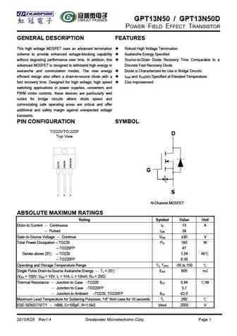
gpt13n50 gpt13n50d.pdf
GPT13N50 / GPT13N50D POWER FIELD EFFECT TRANSISTOR Fig 6. Typical Capacitance Vs. Fig 6. Typical Gate Charge Vs. Gate-to-Source Voltage Drain-to-Source Voltage 2013/6/26 Rev1.4 Greatpower Microelectronic Corp. Page 4 GPT13N50 / GPT13N50D POWER FIELD EFFECT TRANSISTOR PACKAGE DIMENSION TO-220 TO-220F 2013/6/26 Rev1.4 Greatpower Microelectronic Corp. Page 5 GPT13N50 / G
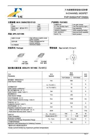
fhp13n50a fhf13n50a.pdf
N N-CHANNEL MOSFET FHP13N50A/FHF13N50A MAIN CHARACTERISTICS FEATURES ID 13A Low gate charge VDSS 500V Crss ( 23pF) Low Crss (typical 23pF ) Rdson-typ @Vgs=10V 0.34 Fast switching Qg-typ 45nC 100% 100% avalanche tested dv/dt Imp
fhp13n50c fhf13n50c.pdf
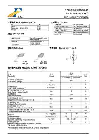
N N-CHANNEL MOSFET FHP13N50C/FHF13N50C MAIN CHARACTERISTICS FEATURES ID 13A Low gate charge VDSS 500V Crss ( 11pF) Low Crss (typical 11pF ) Rdson-typ @Vgs=10V 0.4 Fast switching Qg-typ 40nC 100% 100% avalanche tested dv/dt Impr
hy13n50t.pdf
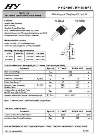
HY13N50T / HY13N50FT 500V / 13A 500V, RDS(ON)=0.52W@VGS=10V, ID=6.5A N-Channel Enhancement Mode MOSFET Features TO-220AB ITO-220AB Low On-State Resistance Fast Switching Low Gate Charge & Low CRSS Fully Characterized Avalanche Voltage and Current Specially Desigened for AC Adapter, Battery Charger and SMPS In compliance with EU RoHs 2002/95/EC Directives 1
jffm13n50e.pdf
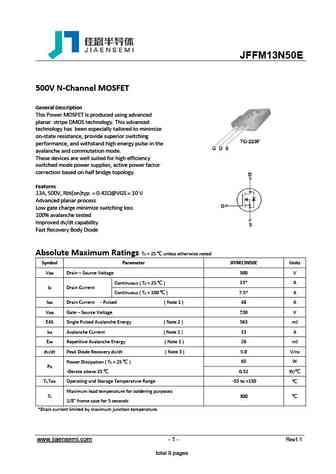
JFFM13N50E 500V N-Channel MOSFET General Description This Power MOSFET is produced using advanced planar stripe DMOS technology. This advanced technology has been especially tailored to minimize on-state resistance, provide superior switching performance, and withstand high energy pulse in the avalanche and commutation mode. These devices are well suited for high efficiency
jfpc13n50c jffm13n50c.pdf
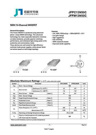
JFPC13N50C JFFM13N50C 500V N-Channel MOSFET General Description Features This Power MOSFET is produced using advanced - 13A, 500V, RDS(on)typ. = 380m @VGS = 10 V planar stripe DMOS technology. This advanced - Low gate charge technology has been especially tailored to minimize - High ruggedness on-state resistance, provide superior switching - Fast switching performanc
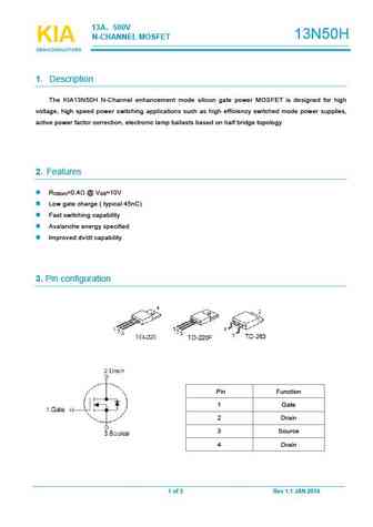
kia13n50h.pdf
13A 500V 13N50H N-CHANNELMOSFET KIA KIA KIA SEMICONDUCTORS SEMICONDUCTORS SEMICONDUCTORS 1. Description The KIA13N50H N-Channel enhancement mode silicon gate power MOSFET is designed for high voltage, high speed power switching applications such as high efficiency switched mode power supplies, active power factor correction, electronic lamp ballasts based on half bridge topology
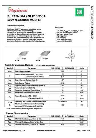
slp13n50a slf13n50a.pdf
LEAD FREE Pb RoHS SLP13N50A / SLF13N50A 500V N-Channel MOSFET General Description Features This Power MOSFET is produced using Maple semi s advanced planar stripe DMOS technology. - 13A, 500V, RDS(on) = 0.483 @VGS = 10 V This advanced technology has been especially tailored - Low gate charge ( typical 19.1nC) to minimize on-state resistance, provide superior switching - Low Crss (
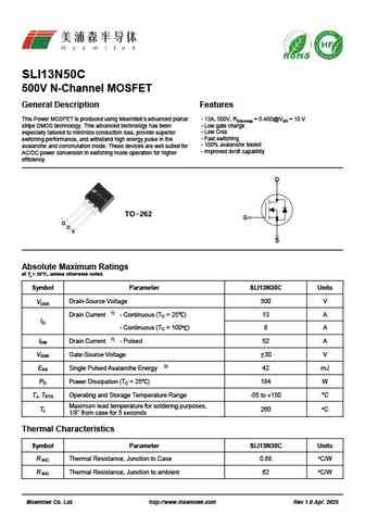
sli13n50c.pdf
SLI13N50C 500V N-Channel MOSFET General Description Features This Power MOSFET is produced using Msemitek s advanced planar - 13A, 500V, RDS(on)typ = 0.48 @VGS = 10 V stripe DMOS technology. This advanced technology has been - Low gate charge especially tailored to minimize conduction loss, provide superior - Low Crss - Fast switching switching performance, and withstand high ener
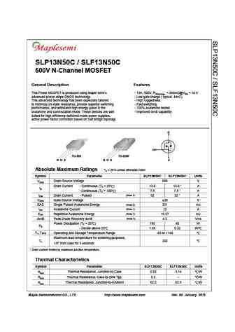
slp13n50c slf13n50c.pdf
SLP13N50C / SLF13N50C 500V N-Channel MOSFET General Description Features This Power MOSFET is produced using Maple semi s - 13A, 500V, RDS(on)typ. = 386m @VGS = 10 V advanced planar stripe DMOS technology. - Low gate charge ( typical 44nC) This advanced technology has been especially tailored - High ruggedness to minimize on-state resistance, provide superior switching - Fast switching
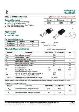
ptp13n50b pta13n50b.pdf
PTP13N50B PTA13N50B 500V N-Channel MOSFET General Features BVDSS RDS(ON),typ. ID Proprietary New Planar Technology 500V 0.40 13A RDS(ON),typ.=0.40 @VGS=10V Low Gate Charge Minimize Switching Loss Fast Recovery Body Diode Applications ATX Power G LCD Panel Power D S G D S Ordering Information Part Number Package Brand TO-220 TO-220F PTP13N50B TO-
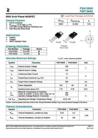
psa13n50 psp13n50.pdf
PSA13N50 PSP13N50 500V N-ch Planar MOSFET General Features BVDSS RDS(ON),Typ. ID RoHS Compliant 500V 0.40 13A RDS(ON),typ.=0.40 @VGS=10V Low Gate Charge Minimize Switching Loss Fast Recovery Body Diode Applications Adaptor Charger SMPS Standby Power Ordering Information Part Number Package Brand PSA13N50 TO-220F PSP13N50 TO-220
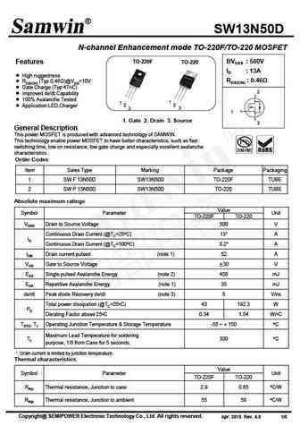
swf13n50d swp13n50d.pdf
SW13N50D N-channel Enhancement mode TO-220F/TO-220 MOSFET TO-220F BVDSS 500V Features TO-220 ID 13A High ruggedness RDS(ON) 0.46 RDS(ON) (Typ 0.46 )@VGS=10V Gate Charge (Typ 47nC) 2 Improved dv/dt Capability 100% Avalanche Tested 1 1 2 2 Application LED,Charger 3 3 1 1. Gate 2. Drain 3. Source 3 General Description Thi
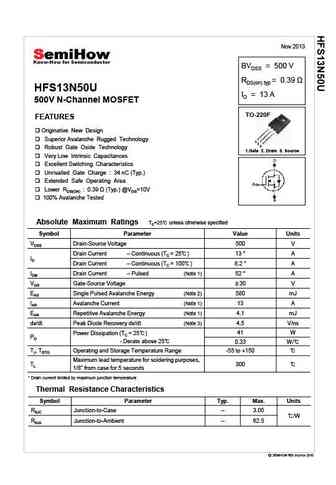
hfs13n50u.pdf
Nov 2013 BVDSS = 500 V RDS(on) typ = 0.39 HFS13N50U ID = 13 A 500V N-Channel MOSFET TO-220F FEATURES Originative New Design Superior Avalanche Rugged Technology 1 2 3 Robust Gate Oxide Technology 1.Gate 2. Drain 3. Source Very Low Intrinsic Capacitances Excellent Switching Characteristics Unrivalled Gate Charge 34 nC (Typ.) Extended Safe Operating Area Lo
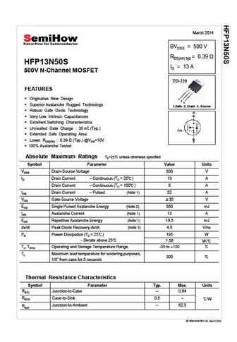
hfp13n50s.pdf
March 2014 BVDSS = 500 V RDS(on) typ HFP13N50S ID = 13 A 500V N-Channel MOSFET TO-220 FEATURES Originative New Design 1 2 3 Superior Avalanche Rugged Technology 1.Gate 2. Drain 3. Source Robust Gate Oxide Technology Very Low Intrinsic Capacitances Excellent Switching Characteristics Unrivalled Gate Charge 38 nC (Typ.) Extended Safe Operating Area L
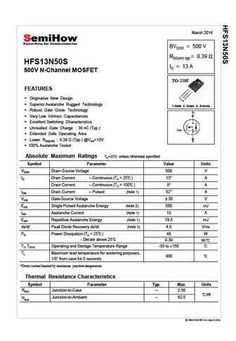
hfs13n50s.pdf
March 2014 BVDSS = 500 V RDS(on) typ HFS13N50S ID = 13 A 500V N-Channel MOSFET TO-220F FEATURES 1 Originative New Design 2 3 Superior Avalanche Rugged Technology 1.Gate 2. Drain 3. Source Robust Gate Oxide Technology Very Low Intrinsic Capacitances Excellent Switching Characteristics Unrivalled Gate Charge 38 nC (Typ.) Extended Safe Operating Area
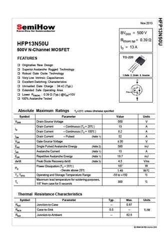
hfp13n50u.pdf
Nov 2013 BVDSS = 500 V RDS(on) typ = 0.39 HFP13N50U ID = 13 A 500V N-Channel MOSFET TO-220 FEATURES Originative New Design Superior Avalanche Rugged Technology 1 2 3 Robust Gate Oxide Technology 1.Gate 2. Drain 3. Source Very Low Intrinsic Capacitances Excellent Switching Characteristics Unrivalled Gate Charge 34 nC (Typ.) Extended Safe Operating Area Low
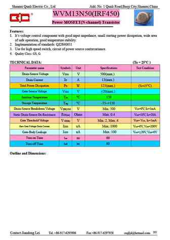
wvm13n50.pdf
Shaanxi Qunli Electric Co., Ltd Add. No. 1 Qunli Road,Baoji City,Shaanxi,China WVM13N50(IRF450) Power MOSFET(N-channel) Transistor Features 1. It s voltage control component with good input impedance, small starting power dissipation, wide area of safe operation, good temperature stability. 2. Implementation of standards QZJ840611 3. Use for high speed switch, circuit of power s
sl13n50fs.pdf
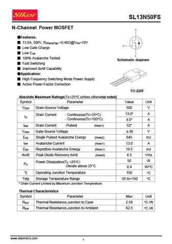
SL13N50FS N-Channel Power MOSFET Features 13.0A, 500V, R =0.40 @V =10V DS(on)(Typ) GS Low Gate Charge Low C rss 100% Avalanche Tested Schematic diagram Fast Switching Improved dv/dt Capability Application High Frequency Switching Mode Power Supply Active Power Factor Correction TO-220F Absolute Maximum Ratings(Tc=25 C unless otherw
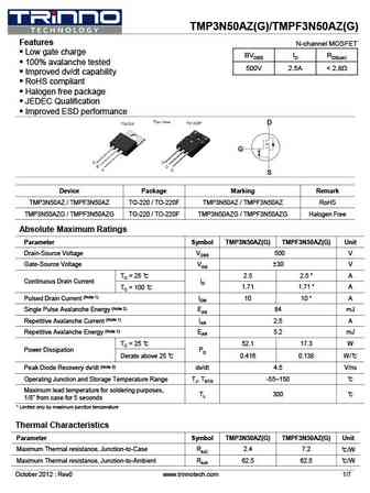
tmp3n50z tmpf3n50z.pdf
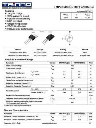
TMP3N50Z(G)/TMPF3N50Z(G) Features N-channel MOSFET Low gate charge BVDSS ID RDS(on) 100% avalanche tested 500V 2.5A
tmp13n50 tmpf13n50.pdf
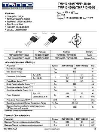
TMP13N50/TMPF13N50 TMP13N50G/TMPF13N50G VDSS = 550 V @Tjmax Features ID = 13A Low gate charge RDS(on) = 0.48 W(max) @ VGS= 10 V 100% avalanche tested Improved dv/dt capability RoHS compliant Halogen free package JEDEC Qualification D G S Device Package Marking Remark TMP13N50 / TMPF13N50 TO-220 / TO-220F TMP13N50 / TMPF13N50 RoHS TMP13N50G / TMPF13N50G
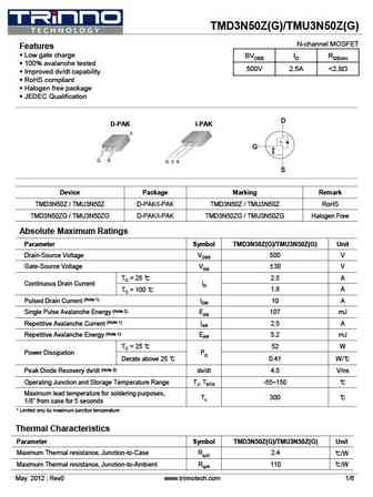
tmd3n50az tmu3n50az.pdf
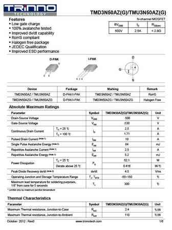
TMD3N50AZ(G)/TMU3N50AZ(G) N-channel MOSFET Features Low gate charge BVDSS ID RDS(on) 100% avalanche tested 500V 2.5A
tmp3n50az tmpf3n50az.pdf
TMP3N50AZ(G)/TMPF3N50AZ(G) Features N-channel MOSFET Low gate charge BVDSS ID RDS(on) 100% avalanche tested 500V 2.5A
tman23n50a.pdf
TMAN23N50A N-channel MOSFET Features BVDSS ID RDS(on) Low gate charge 500V 23A
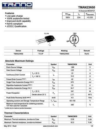
tman23n50.pdf
TMAN23N50 N-channel MOSFET Features BVDSS ID RDS(on)MAX Low gate charge 500V 23A
tmd3n50z tmu3n50z.pdf
TMD3N50Z(G)/TMU3N50Z(G) N-channel MOSFET Features Low gate charge BVDSS ID RDS(on) 100% avalanche tested 500V 2.5A
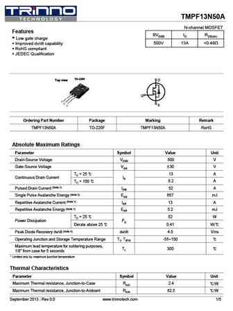
tmpf13n50a.pdf
TMPF13N50A N-channel MOSFET Features BVDSS ID RDS(on) Low gate charge 500V 13A
tsp13n50m tsf13n50m.pdf
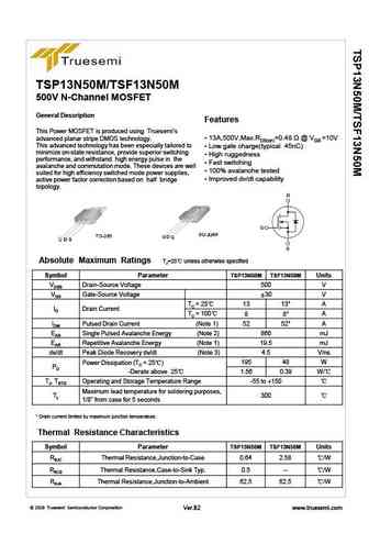
TSP13N50M/TSF13N50M 500V N-Channel MOSFET General Description Features This Power MOSFET is produced using Truesemi s 13A,500V,Max.RDS(on)=0.48 @ VGS =10V advanced planar stripe DMOS technology. This advanced technology has been especially tailored to Low gate charge(typical 45nC) minimize on-state resistance, provide superior switching High ruggedness perfo
tsa23n50m.pdf
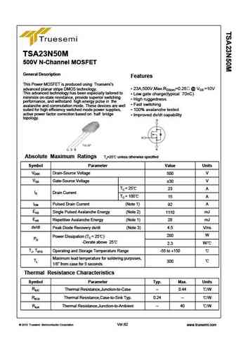
TSA23N50M 500V N-Channel MOSFET General Description Features This Power MOSFET is produced using Truesemi s advanced planar stripe DMOS technology. 23A,500V,Max.RDS(on)=0.26 @ VGS =10V This advanced technology has been especially tailored to Low gate charge(typical 70nC) minimize on-state resistance, provide superior switching High ruggedness performance, and withstand
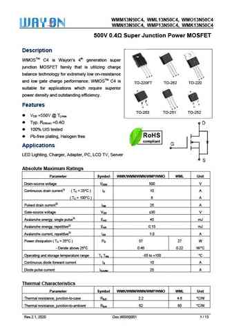
wmm13n50c4 wml13n50c4 wmo13n50c4 wmn13n50c4 wmp13n50c4 wmk13n50c4.pdf
WMM13N50C4, WML13N5 WM C4 50C4, MO13N50C WMN13N50C4, WMP13N5 WM C4 50C4, MK13N50C 500V 0.4 S unction Power M T V Super Ju MOSFET Descrip ption WMOSTM C4 is Wa 4th generation super ayon s n junction MOSFET fa that is utilizing charge M amily S balance te or extremely esistance echnology fo y low on-re D S D G G G S D G and low ga charge performanc WMO
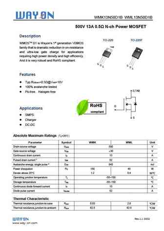
wmk13n50d1b wml13n50d1b.pdf
WMK13N50D1B WML13N50D1B 500V 13A 0.5 N-ch Power MOSFET Description TO-220 TO-220F WMOSTM D1 is Wayon s 1st generation VDMOS TAB family that is dramatic reduction in on-resistance and ultra-low gate charge for applications requiring high power density and high efficiency. And it is very robust and RoHS compliant. G D S G D S Features Typ.R =0.5 @V =10V DS(
cs13n50fa9h.pdf
Silicon N-Channel Power MOSFET R CS13N50F A9H VDSS 500 V General Description ID 13 A CS13N50F A9H, the silicon N-channel Enhanced PD (TC=25 ) 60 W VDMOSFETs, is obtained by the self-aligned planar RDS(ON)Typ 0.34 Technology which reduce the conduction loss, improve switching performance and enhance the avalanche energy. The transistor can be used in variou
cs3n50b3hy.pdf
Silicon N-Channel Power MOSFET R CS3N50 B3HY General Description VDSS 500 V CS3N50 B3HY, the silicon N-channel Enhanced ID 3 A VDMOSFETs, is obtained by the self-aligned planar PD (TC=25 ) 35 W RDS(ON)Typ 2.4 Technology which reduce the conduction loss, improve switching performance and enhance the avalanche energy. The transistor can be used in various powe
cs3n50b4hy.pdf
Silicon N-Channel Power MOSFET R CS3N50 B4HY General Description VDSS 500 V CS3N50 B4HY, the silicon N-channel Enhanced ID 3 A PD (TC=25 ) 35 W VDMOSFETs, is obtained by the self-aligned planar Technology RDS(ON)Typ 2.4 which reduce the conduction loss, improve switching performance and enhance the avalanche energy. The transistor can be used in various po
cs13n50fa9r.pdf
Silicon N-Channel Power MOSFET R CS13N50F A9R General Description VDSS 500 V CS13N50F A9R, the silicon N-channel Enhanced ID 13 A PD(TC=25 ) 42 W VDMOSFETs, is obtained by the self-aligned planar Technology RDS(ON)Typ 0.4 which reduce the conduction loss, improve switching performance and enhance the avalanche energy. The transistor can be used in various po
cs13n50a8h.pdf
Silicon N-Channel Power MOSFET R CS13N50 A8H VDSS 500 V General Description ID 13 A CS13N50 A8H, the silicon N-channel Enhanced PD (TC=25 ) 150 W VDMOSFETs, is obtained by the self-aligned planar Technology RDS(ON)Typ 0.34 which reduce the conduction loss, improve switching performance and enhance the avalanche energy. The transistor can be used in various p
cs3n50df cs3n50dp cs3n50dd cs3n50du.pdf
CS3N50DF, CS3N50DP, nvert Suzhou Convert Semiconductor Co ., Ltd. CS3N50DD,CS3N50DU 500V N-Channel MOSFET FEATURES Fast switching 100% avalanche tested Improved dv/dt capability APPLICATIONS Switch Mode Power Supply (SMPS) Uninterruptible Power Supply (UPS) Power Factor Correction (PFC) Device Marking and Package Information Device Package Marking CS3N50DF
fir13n50fg.pdf
FIR13N50FG CREAT BY ART Advanced N-Ch Power MOSFET-G PIN Connection TO-220F VDSS 500 V ID 13 A PD (TC=25 ) 150 W RDS(ON) 0.4 G D S Features Fast Switching g Schematic dia ram Low ON Resistance(Rdson 0.5 ) D Low Gate Charge (Typical Data 85nC) Low Reverse transfer capacitances(Typical 100pF) G 100% Single Pulse avalanche energy Test S Marking Di
hfs13n50.pdf
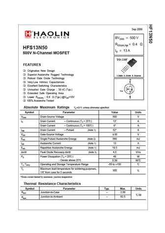
Sep 2009 BVDSS = 500 V RDS(on) typ = 0.4 HFS13N50 ID = 13 A 500V N-Channel MOSFET TO-220F FEATURES 1 Originative New Design 2 3 Superior Avalanche Rugged Technology 1.Gate 2. Drain 3. Source Robust Gate Oxide Technology Very Low Intrinsic Capacitances Excellent Switching Characteristics Unrivalled Gate Charge 38 nC (Typ.) Unrivalled Gate Charge 38 nC (Typ ) Ext
jmpc13n50bj.pdf
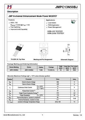
JMPC13N50BJ Description JMP N-channel Enhancement Mode Power MOSFET Features Applications 500V, 13A Load Switch RDS(ON)
jmpf13n50bj.pdf
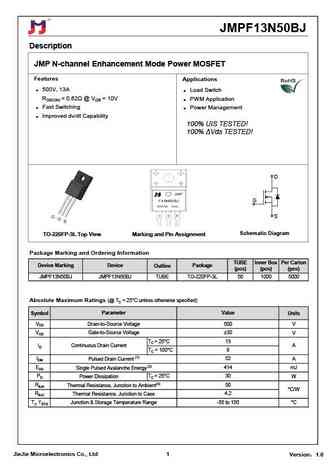
JMPF13N50BJ Description JMP N-channel Enhancement Mode Power MOSFET Features Applications 500V, 13A Load Switch RDS(ON)
lnc13n50 lnd13n50.pdf
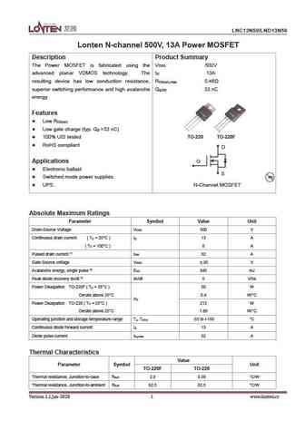
LNC13N50/LND13N50 Lonten N-channel 500V, 13A Power MOSFET Description Product Summary The Power MOSFET is fabricated using the V 500V DSS advanced planar VDMOS technology. The I 13A D resulting device has low conduction resistance, R 0.46 DS(on),max superior switching performance and high avalanche Q 33 nC g,typ energy. Features Low R DS(on) Low gate charge (typ. Q =33
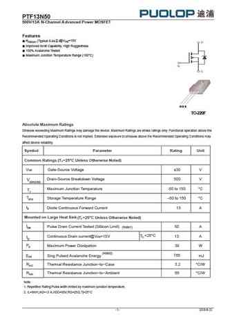
ptf13n50.pdf
PTF1 3 N5 0 5 00V/1 3 A N-Channel A dv anced Power MOSFET Features )@VGS=10V RDS(on) (Typical 0.44 Improved dv/dt Capability, High Ruggedness 100% Avalanche Tested Maximum Junction Temperature Range (150 C) G D S TO-220F Absolute Maximum Ratings Stresses exceeding Maximum Ratings may damage the device. Maximum Ratings are stress ratings only. Functional operation
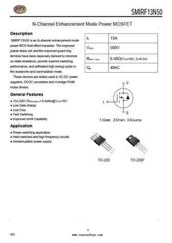
smirf13n50.pdf
SMIRF13N50 30V /36A Single N Power MOSFET N-Channel Enhancement Mode Power MOSFET Description ID 13A SMIRF13N50 is an N-channel enhancement mode power MOS field effect transistor. The improved VDSS 500V planar stripe cell and the improved guard ring terminal have been especially tailored to minimize Rdson max 0.48 (VGS=10V, ID=6.5A) on-state resistance, provide superi
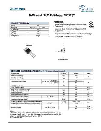
vbzm13n50.pdf
VBZM13N50 www.VBsemi.com N hannel 500 D S Power MOSFET FEATURES PRODUCT SUMMARY Lower Gate Charge Qg Results in Simpler Drive VDS (V) 500 Reqirements RDS(on) ( )VGS = 10 V 0.660 Improved Gate, Avalanche and Dynamic dV/dt Qg (Max.) (nC) 81 Ruggedness Qgs (nC) 20 Qgd (nC) 36 Fully Characterized Capacitance and Avalanche Voltage Configuration Single Complian
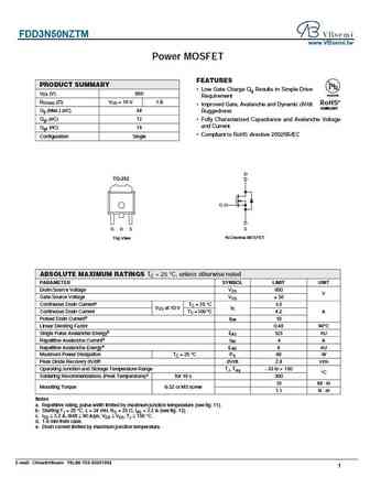
fdd3n50nztm.pdf
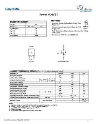
FDD3N50NZTM www.VBsemi.tw Power MOSFET FEATURES PRODUCT SUMMARY Low Gate Charge Qg Results in Simple Drive VDS (V) 650 Available Requirement RDS(on) ( )VGS = 10 V 1.8 RoHS* Improved Gate, Avalanche and Dynamic dV/dt COMPLIANT Qg (Max.) (nC) 48 Ruggedness Qgs (nC) 12 Fully Characterized Capacitance and Avalanche Voltage and Current Qgd (nC) 19 Compliant to RoH
aot13n50.pdf
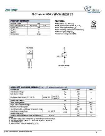
AOT13N50 www.VBsemi.tw N-Channel 650 V (D-S) MOSFET PRODUCT SUMMARY FEATURES VDS (V) at TJ max. 650 Reduced trr, Qrr, and IRRM RDS(on) max. ( ) at 25 C VGS = 10 V 0.34 Low figure-of-merit (FOM) Ron x Qg Qg max. (nC) 106 Low input capacitance (Ciss) Qgs (nC) 14 Low switching losses due to reduced Qrr Ultra low gate charge (Qg) Qgd (nC) 33 Avalanche ener
fdd3n50nz.pdf
FDD3N50NZ www.VBsemi.tw Power MOSFET FEATURES PRODUCT SUMMARY Low Gate Charge Qg Results in Simple Drive VDS (V) 650 Available Requirement RDS(on) ( )VGS = 10 V 1.8 RoHS* Improved Gate, Avalanche and Dynamic dV/dt COMPLIANT Qg (Max.) (nC) 48 Ruggedness Qgs (nC) 12 Fully Characterized Capacitance and Avalanche Voltage and Current Qgd (nC) 19 Compliant to RoHS
vbzmb13n50.pdf
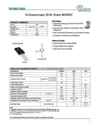
VBZMB13N50 www.VBsemi.com N-Channel (D-S) Power MOSFET 500V FEATURES PRODUCT SUMMARY Lower Gate Charge Qg Results in Simpler Drive VDS (V) 500 Available Reqirements RDS(on) ( )VGS = 10 V 0.80 Improved Gate, Avalanche and Dynamic dV/dt Available Qg (Max.) (nC) 81 Ruggedness Qgs (nC) 20 Qgd (nC) 36 Fully Characterized Capacitance and Avalanche Voltage Configuratio
hm13n50 hm13n50f.pdf
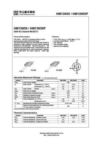
HM13N50 / HM13N50F HM13N50 / HM13N50F 500V N-Channel MOSFET General Description Features This Power MOSFET is produced using SL semi s 13.0A, 500V, RDS(on) = 0.48 @VGS = 10 V advanced planar stripe DMOS technology. Low gate charge ( typical 45nC) This advanced technology has been espe cially tailored to Fast witching s minimize o n-state r esistance, pr ovide superior
mp13n50.pdf
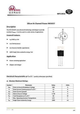
MP13N50 SiliconN-Channel Power MOSFET Description TheMP13N50PF uses advancedtechnology anddesigntoprovide excellent R . It canbeusedinawidevariety of applications. DS(ON) General Features V =500V,I =13A DS D LowONResistance LowReversetransfer capacitances 100%SinglePulseavalancheenergy Test Application Power switchingapplication Adapter andcharger Electrical Characteristics
mpf13n50.pdf
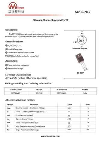
Silicon N-Channel Power MOSFET Description The MPF13N50 uses advanced technology and design to provide excellent RDS(ON) . It can be used in a wide variety of applications. General Features V =500V,I =13A DS D Schematic diagram Low ON Resistance Low Reverse transfer capacitances 100% Single Pulse avalanche energy Test Application Power switching application Adapte
md23n50.pdf
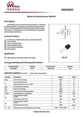
Silicon N-Channel Power MOSFET Description MD23N50 the silicon N-channel Enhanced MOSFETs, is obtained by advanced MOSFET technology which reduce the conduction loss, improve switching performance and enhance the avalanche energy. The transistor is suitable device for SMPS, high speed switching and general purpose applications. General Features 1 V =500V, R
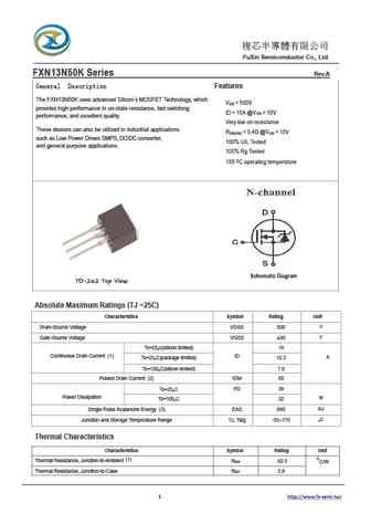
fxn13n50c.pdf
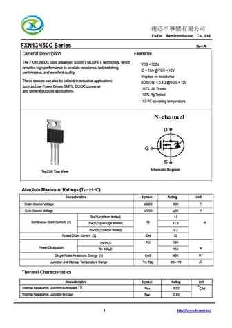
FuXin Semiconductor Co., Ltd. FXN13N50C Series Rev.A General Description Features The FXN13N50C uses advanced Silicon s MOSFET Technology, which VDS = 500V provides high performance in on-state resistance, fast switching ID = 13A @VGS = 10V performance, and excellent quality. Very low on-resistance These devices can also be utilized in indust
fxn13n50k.pdf
FuXin Semiconductor Co., Ltd. FXN13N50K Series Rev.A General Description Features The FXN13N50K uses advanced Silicon s MOSFET Technology, which V = 500V DS provides high performance in on-state resistance, fast switching ID = 15A @V = 10V GS performance, and excellent quality. Very low on-resistance These devices can also be utilized in industrial a
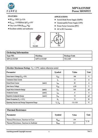
mpva13n50f.pdf
MPVA13N50F Power MOSFET MPSW60M041 FEATURES APPLICATIONS l BVDSS 500V, ID=13A l Switch Mode Power Supply (SMPS) l RDS(on) 0.45 (Max) @VGS=10V l Uninterruptible Power Supply (UPS) l Very Low FOM (RDS(on) *Qg) l Power Factor Correction (PFC) l Excellent stability and uniformity l AC to DC Converters D G S TO-220F Ordering Information Type NO. Marking Package Code MPVA13N5
mdp13n50th.pdf
isc N-Channel MOSFET Transistor MDP13N50TH FEATURES Drain Current I = 13A@ T =25 D C Drain Source Voltage V = 500V(Min) DSS Static Drain-Source On-Resistance R = 0.5 (Max) @V = 10V DS(on) GS 100% avalanche tested Minimum Lot-to-Lot variations for robust device performance and reliable operation DESCRIPTION motor drive, DC-DC converter, power switch and solen
mtp3n50e.pdf
INCHANGE Semiconductor isc N-Channel MOSFET Transistor MTP3N50E FEATURES With TO-220 packaging High speed switching Very high commutation ruggedness Easy to use 100% avalanche tested Minimum Lot-to-Lot variations for robust device performance and reliable operation APPLICATIONS PFC stages Popular AC-DC applications Power supply Switching applications ABS
irfp23n50l.pdf
iscN-Channel MOSFET Transistor IRFP23N50L FEATURES Low drain-source on-resistance RDS(ON) =0.235 (MAX) Enhancement mode Vth = 3.0 to 5.0V (VDS = 10 V, ID=0.25mA) 100% avalanche tested Minimum Lot-to-Lot variations for robust device performance and reliable operation DESCRITION Switching Voltage Regulators ABSOLUTE MAXIMUM RATINGS(T =25 ) a SYMBOL PARAMETER VA
aotf3n50.pdf
isc N-Channel MOSFET Transistor AOTF3N50 FEATURES Drain Current I = 3.0A@ T =25 D C Drain Source Voltage- V =500V(Min) DSS Static Drain-Source On-Resistance R =3.0 (Max) DS(on) 100% avalanche tested Minimum Lot-to-Lot variations for robust device performance and reliable operation DESCRIPTION Designed for use in switch mode power supplies and general purpos
aod3n50.pdf
isc N-Channel MOSFET Transistor AOD3N50 FEATURES Drain Current I = 2.8A@ T =25 D C Drain Source Voltage- V =500V(Min) DSS Static Drain-Source On-Resistance R =3.0 (Max) DS(on) 100% avalanche tested Minimum Lot-to-Lot variations for robust device performance and reliable operation DESCRIPTION Designed for use in switch mode power supplies and general purpose
aot13n50.pdf
isc N-Channel MOSFET Transistor AOT13N50 FEATURES Drain Current I = 13A@ T =25 D C Drain Source Voltage- V = 500V(Min) DSS Static Drain-Source On-Resistance R = 0.51 (Max) DS(on) 100% avalanche tested Minimum Lot-to-Lot variations for robust device performance and reliable operation DESCRIPTION Designed for use in switch mode power supplies and general purp
mdq23n50dtp.pdf
isc N-Channel MOSFET Transistor MDQ23N50DTP FEATURES Drain Current I = 23A@ T =25 D C Drain Source Voltage V = 500V(Min) DSS Static Drain-Source On-Resistance R = 0.245 (Max) @V = 10V DS(on) GS 100% avalanche tested Minimum Lot-to-Lot variations for robust device performance and reliable operation DESCRIPTION motor drive, DC-DC converter, power switch and so
23n50.pdf
isc N-Channel MOSFET Transistor 23N50 FEATURES Drain Current I = 23A@ T =25 D C Drain Source Voltage- V =500V(Min) DSS Static Drain-Source On-Resistance R =0.245 (Max) DS(on) 100% avalanche tested Minimum Lot-to-Lot variations for robust device performance and reliable operation DESCRIPTION Designed for use in switch mode power supplies and general purpose
aou3n50.pdf
isc N-Channel MOSFET Transistor AOU3N50 FEATURES Drain Current I = 2.8A@ T =25 D C Drain Source Voltage- V =500V(Min) DSS Static Drain-Source On-Resistance R =3.0 (Max) DS(on) 100% avalanche tested Minimum Lot-to-Lot variations for robust device performance and reliable operation DESCRIPTION Designed for use in switch mode power supplies and general purpose
fqpf13n50cf.pdf
isc N-Channel MOSFET Transistor FQPF13N50CF FEATURES Drain Current I =13A@ T =25 D C Drain Source Voltage V =500V(Min) DSS Static Drain-Source On-Resistance R =0.54m (Max) @ V = 10V DS(on) GS 100% avalanche tested Minimum Lot-to-Lot variations for robust device performance and reliable operation DESCRIPTION motor drive, DC-DC converter, power switch and sole
aotf13n50.pdf
isc N-Channel MOSFET Transistor AOTF13N50 FEATURES Drain Current I = 13A@ T =25 D C Drain Source Voltage- V = 500V(Min) DSS Static Drain-Source On-Resistance R = 0.51 (Max) DS(on) 100% avalanche tested Minimum Lot-to-Lot variations for robust device performance and reliable operation DESCRIPTION Designed for use in switch mode power supplies and general pur
aot3n50.pdf
isc N-Channel MOSFET Transistor AOT3N50 FEATURES Drain Current I = 3.0A@ T =25 D C Drain Source Voltage- V =500V(Min) DSS Static Drain-Source On-Resistance R =3.0 (Max) DS(on) 100% avalanche tested Minimum Lot-to-Lot variations for robust device performance and reliable operation DESCRIPTION Designed for use in switch mode power supplies and general purpose
fmh23n50e.pdf
isc N-Channel MOSFET Transistor FMH23N50E FEATURES With TO-3PN packaging High speed switching Standard level gate drive Easy to use 100% avalanche tested Minimum Lot-to-Lot variations for robust device performance and reliable operation APPLICATIONS Power supply Switching applications ABSOLUTE MAXIMUM RATINGS(T =25 ) a SYMBOL PARAMETER VALUE UNIT V Drain-S
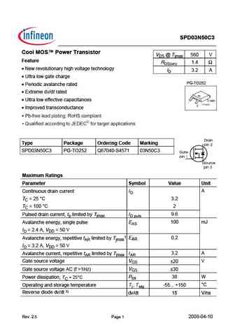
spd03n50c3.pdf
isc N-Channel MOSFET Transistor SPD03N50C3, ISPD03N50C3 FEATURES Static drain-source on-resistance RDS(on) 1.4 Enhancement mode 100% avalanche tested Minimum Lot-to-Lot variations for robust device performance and reliable operation DESCRITION Improved transconductance ABSOLUTE MAXIMUM RATINGS(T =25 ) a SYMBOL PARAMETER VALUE UNIT V Drain-Source Voltage 560
irfb13n50a.pdf
iscN-Channel MOSFET Transistor IRFB13N50A FEATURES Low drain-source on-resistance RDS(ON) =0.45 (MAX) Enhancement mode Vth = 2.0 to 4.0V (VDS = 10 V, ID=0.25mA) 100% avalanche tested Minimum Lot-to-Lot variations for robust device performance and reliable operation DESCRITION Switching Voltage Regulators ABSOLUTE MAXIMUM RATINGS(T =25 ) a SYMBOL PARAMETER VAL
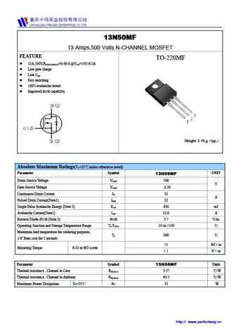
13n50mf.pdf
13N50MF 13 Amps,500 Volts N-CHANNEL MOSFET FEATURE TO-220MF 13A,500V,R =0.48 @V =10V/6.5A DS(ON)MAX GS Low gate charge Low C iss Fast switching 100% avalanche tested Improved dv/dt capability Weight 2.16 g typ. Absolute Maximum Ratings(T =25 ,unless otherwise noted) C Parameter Symbol UNIT 13N50MF Drain-Source Voltage V 500 DSS V Gate-Source
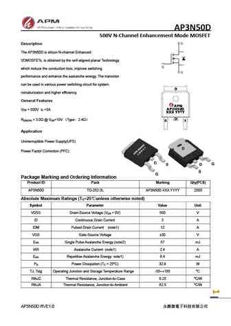
ap3n50d.pdf
AP3N50D 500V N-Channel Enhancement Mode MOSFET Description The AP3N50D is silicon N-channel Enhanced VDMOSFETs, is obtained by the self-aligned planar Technology which reduce the conduction loss, improve switching performance and enhance the avalanche energy. The transistor can be used in various power switching circuit for system miniaturization and higher efficiency. Genera
Другие MOSFET... UF830Z , UF840 , UK3568 , UF450 , UF460 , 1N50 , 1N50Z , 2N50 , AO3401 , 3N50Z , 4N50 , 5N50 , 5N50K , 6N50 , 7N50 , 8N50 , 1N40 .
🌐 : EN ES РУ
Список транзисторов
Обновления
MOSFET: HAF1008S | HAF1008L | EMZB08P03H | CS30N20FA9R | AOT66613L | AOSP21313C | AOSP21311C | AOB66918L | AO3415C | AOTF20N40L | AOTF11N60L | AOT11N60L | AONS21303C | AOI280A60 | AOB66914L | AO3485C
Popular searches
2sc1885 | skd502t | 2sb754 | 2sc2362 | 2sd468 | c2240 transistor | 2sc1918 | c1213 transistor
