4N50 datasheet, аналоги, основные параметры
Наименование производителя: 4N50 📄📄
Тип транзистора: MOSFET
Полярность: N
Предельные значения
Pd ⓘ - Максимальная рассеиваемая мощность: 85 W
|Vds|ⓘ - Максимально допустимое напряжение сток-исток: 500 V
|Vgs|ⓘ - Максимально допустимое напряжение затвор-исток: 30 V
|Id| ⓘ - Максимально допустимый постоянный ток стока: 4 A
Tj ⓘ - Максимальная температура канала: 150 °C
Электрические характеристики
tr ⓘ - Время нарастания: 21 ns
Cossⓘ - Выходная емкость: 65 pf
RDSonⓘ - Сопротивление сток-исток открытого транзистора: 1.6 Ohm
📄📄 Копировать
Аналог (замена) для 4N50
- подборⓘ MOSFET транзистора по параметрам
4N50 даташит
4n50.pdf
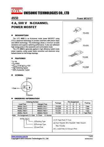
UNISONIC TECHNOLOGIES CO., LTD 4N50 Power MOSFET 4 A, 500 V N-CHANNEL POWER MOSFET 1 TO-252 DESCRIPTION The UTC 4N50 is an N-channel mode power MOSFET using UTC s advanced technology to provide customers with planar stripe and DMOS technology. This technology allows a minimum on-state 1 resistance and superior switching performance. It also can withstand TO-251 hig
spa04n50c3 spb04n50c3 spp04n50c3.pdf
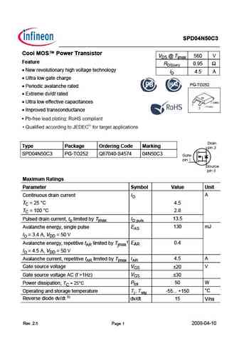
SPP04N50C3, SPB04N50C3 Final data SPA04N50C3 Cool MOS Power Transistor VDS @ Tjmax 560 V Feature RDS(on) 0.95 New revolutionary high voltage technology ID 4.5 A Ultra low gate charge P-TO220-3-31 P-TO263-3-2 P-TO220-3-1 Periodic avalanche rated Extreme dv/dt rated 3 Ultra low effective capacitances 2 1 P-TO220-3-31 Improved transconductance
mtp4n50erev1a.pdf
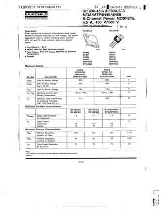
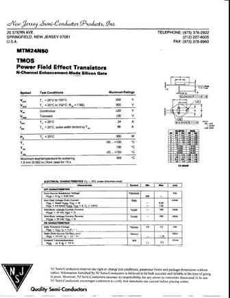
MOTOROLA Order this document SEMICONDUCTOR TECHNICAL DATA by MTP4N50E/D Designer's Data Sheet MTP4N50E TMOS E-FET. Motorola Preferred Device High Energy Power FET N Channel Enhancement Mode Silicon Gate TMOS POWER FET This advanced high voltage TMOS E FET is designed to 4.0 AMPERES withstand high energy in the avalanche mode and switch efficiently. 500 VOLTS This new
mtw14n50e.pdf
MOTOROLA Order this document SEMICONDUCTOR TECHNICAL DATA by MTW14N50E/D Designer's Data Sheet MTW14N50E TMOS E-FET. Motorola Preferred Device Power Field Effect Transistor TO-247 with Isolated Mounting Hole TMOS POWER FET N Channel Enhancement Mode Silicon Gate 14 AMPERES 500 VOLTS This advanced TMOS E FET is designed to withstand high RDS(on) = 0.40 OHM energy in th
mtp4n50e.pdf

MOTOROLA Order this document SEMICONDUCTOR TECHNICAL DATA by MTP4N50E/D Designer's Data Sheet MTP4N50E TMOS E-FET. Motorola Preferred Device High Energy Power FET N Channel Enhancement Mode Silicon Gate TMOS POWER FET This advanced high voltage TMOS E FET is designed to 4.0 AMPERES withstand high energy in the avalanche mode and switch efficiently. 500 VOLTS This new
mtw14n50erev4.pdf

MOTOROLA Order this document SEMICONDUCTOR TECHNICAL DATA by MTW14N50E/D Designer's Data Sheet MTW14N50E TMOS E-FET. Motorola Preferred Device Power Field Effect Transistor TO-247 with Isolated Mounting Hole TMOS POWER FET N Channel Enhancement Mode Silicon Gate 14 AMPERES 500 VOLTS This advanced TMOS E FET is designed to withstand high RDS(on) = 0.40 OHM energy in th
irfba34n50c.pdf
PD- 93931 PROVISIONAL IRFBA34N50C SMPS MOSFET HEXFET Power MOSFET Applications VDSS RDS(on) typ. ID Switch Mode Power Supply (SMPS) UninterruptIble Power Supply 500V 0.070 40A High Speed Power Switching Benefits Low Gate Charge Qg results in Simple Drive Requirement Improved Gate, Avalanche and Dynamic dv/dt Ruggedness Fully Characterized Capacitance and Super-220
phw14n50e 3.pdf
Philips Semiconductors Product specification PowerMOS transistors PHW14N50E Avalanche energy rated FEATURES SYMBOL QUICK REFERENCE DATA d Repetitive Avalanche Rated Fast switching VDSS = 500 V Stable off-state characteristics High thermal cycling performance ID = 14 A g Low thermal resistance RDS(ON) 0.4 s GENERAL DESCRIPTION PINNING SOT429 (TO247) N
phx4n50e 1.pdf
Philips Semiconductors Objective specification PowerMOS transistor PHX4N50E Isolated version of PHP4N50E GENERAL DESCRIPTION QUICK REFERENCE DATA N-channel enhancement mode SYMBOL PARAMETER MAX. UNIT field-effect power transistor in a full pack, plastic envelope featuring high VDS Drain-source voltage 500 V avalanche energy capability, stable ID Drain current (DC) 2.9 A blocking volt
php4n50e 1.pdf
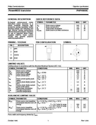
Philips Semiconductors Objective specification PowerMOS transistor PHP4N50E GENERAL DESCRIPTION QUICK REFERENCE DATA N-channel enhancement mode SYMBOL PARAMETER MAX. UNIT field-effect power transistor in a plastic envelope featuring high VDS Drain-source voltage 500 V avalanche energy capability, stable ID Drain current (DC) 5.3 A blocking voltage, fast switching and Ptot Total power d

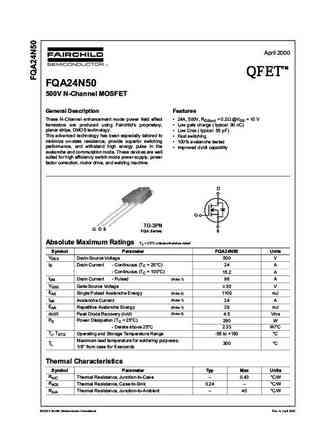
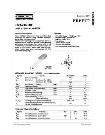
fqa24n50.pdf
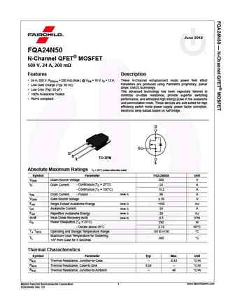
June 2014 FQA24N50 N-Channel QFET MOSFET 500 V, 24 A, 200 m Features Description 24 A, 500 V, RDS(on) = 200 m (Max.) @ VGS = 10 V, ID = 12 A These N-Channel enhancement mode power field effect transistors are produced using Fairchild s proprietary, planar Low Gate Charge (Typ. 90 nC) stripe, DMOS technology. Low Crss (Typ. 55 pF) This advanced technology has been e
fqd4n50tf fqd4n50tm fqd4n50 fqu4n50.pdf
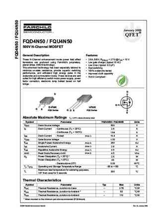
January 2009 QFET FQD4N50 / FQU4N50 500V N-ChanneI MOSFET GeneraI Description Features These N-Channel enhancement mode power field effect 2.6A, 500V, RDS(on) = 2.7 @VGS = 10 V transistors are produced using Fairchild s proprietary, Low gate charge ( typical 10 nC) planar stripe, DMOS technology. Low Crss ( typical 6.0 pF) This advanced technology has been especiall
fqp4n50.pdf
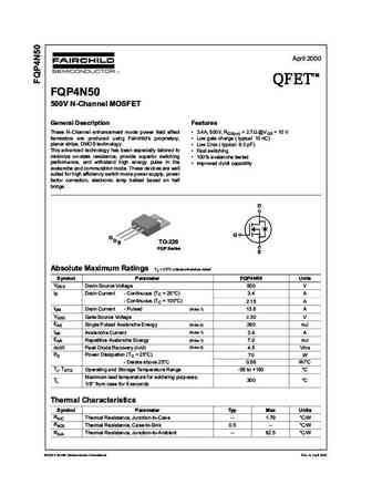
April 2000 TM QFET QFET QFET QFET 500V N-ChanneI MOSFET GeneraI Description Features These N-Channel enhancement mode power field effect 3.4A, 500V, RDS(on) = 2.7 @VGS = 10 V transistors are produced using Fairchild s proprietary, Low gate charge ( typical 10 nC) planar stripe, DMOS technology. Low Crss ( typical 6.0 pF) This advanced technology has been
fqb4n50tm.pdf
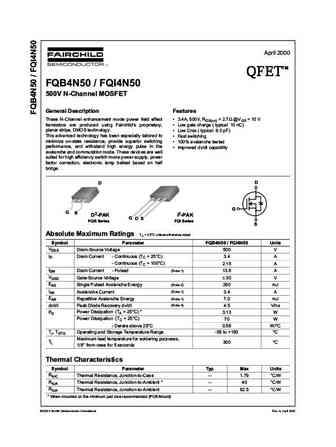
April 2000 TM QFET QFET QFET QFET FQB4N50 / FQI4N50 500V N-ChanneI MOSFET GeneraI Description Features These N-Channel enhancement mode power field effect 3.4A, 500V, RDS(on) = 2.7 @VGS = 10 V transistors are produced using Fairchild s proprietary, Low gate charge ( typical 10 nC) planar stripe, DMOS technology. Low Crss ( typical 6.0 pF) This advanced technology
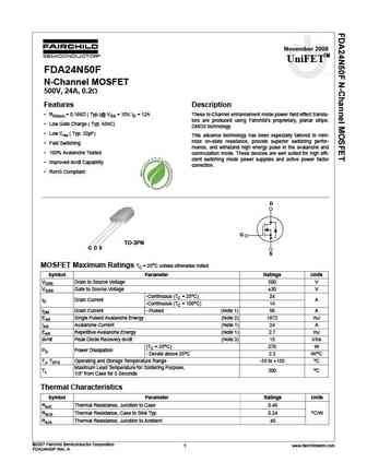
fda24n50.pdf
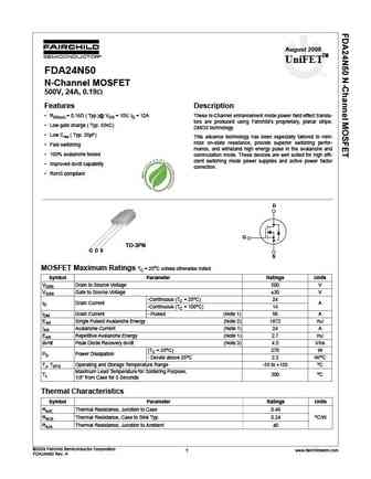
August 2008 UniFETTM FDA24N50 N-Channel MOSFET 500V, 24A, 0.19 Features Description RDS(on) = 0.16 ( Typ.)@ VGS = 10V, ID = 12A These N-Channel enhancement mode power field effect transis- tors are produced using Fairchild s proprietary, planar stripe, Low gate charge ( Typ. 65nC) DMOS technology. Low Crss ( Typ. 35pF) This advance technology has been especially t
fqa24n50 f109.pdf
April 2000 TM QFET QFET QFET QFET 500V N-ChanneI MOSFET GeneraI Description Features These N-Channel enhancement mode power field effect 24A, 500V, RDS(on) = 0.2 @VGS = 10 V transistors are produced using Fairchild s proprietary, Low gate charge ( typical 90 nC) planar stripe, DMOS technology. Low Crss ( typical 55 pF) This advanced technology has been e
fqa24n50f.pdf
September 2001 TM FRFET FQA24N50F 500V N-Channel MOSFET General Description Features These N-Channel enhancement mode power field effect 24A, 500V, RDS(on) = 0.2 @VGS = 10 V transistors are produced using Fairchild s proprietary, Low gate charge ( typical 90 nC) planar stripe, DMOS technology. Low Crss ( typical 55 pF) This advanced technology has been especially tail
fdh44n50.pdf
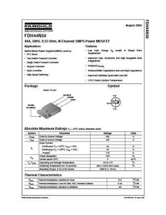
August 2002 FDH44N50 44A, 500V, 0.12 Ohm, N-Channel SMPS Power MOSFET Applications Features Low Gate Charge Qg results in Simple Drive Switch Mode Power Supplies(SMPS), such as Requirement PFC Boost Improved Gate, Avalanche and High Reapplied dv/dt Two-Switch Forward Converter Ruggedness Single Switch Forward Converter Reduced rDS(ON) Flyback Converter
fda24n50f.pdf
November 2008 UniFETTM FDA24N50F tm N-Channel MOSFET 500V, 24A, 0.2 Features Description RDS(on) = 0.166 ( Typ.)@ VGS = 10V, ID = 12A These N-Channel enhancement mode power field effect transis- tors are produced using Fairchild s proprietary, planar stripe, Low Gate Charge ( Typ. 65nC) DMOS technology. Low Crss ( Typ. 32pF) This advance technology has been esp
fqpf4n50.pdf
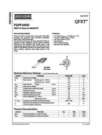
April 2000 TM QFET QFET QFET QFET 500V N-ChanneI MOSFET GeneraI Description Features These N-Channel enhancement mode power field effect 2.3A, 500V, RDS(on) = 2.7 @VGS = 10 V transistors are produced using Fairchild s proprietary, Low gate charge ( typical 10 nC) planar stripe, DMOS technology. Low Crss ( typical 6.0 pF) This advanced technology has been
sihg14n50d.pdf
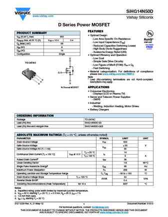
SiHG14N50D www.vishay.com Vishay Siliconix D Series Power MOSFET FEATURES PRODUCT SUMMARY Optimal Design VDS (V) at TJ max. 550 - Low Area Specific On-Resistance RDS(on) max. at 25 C ( ) VGS = 10 V 0.4 - Low Input Capacitance (Ciss) Qg (Max.) (nC) 58 - Reduced Capacitive Switching Losses Qgs (nC) 8 - High Body Diode Ruggedness Qgd (nC) 14 - Avalanche Energy Rated (UIS)
sihp14n50d.pdf
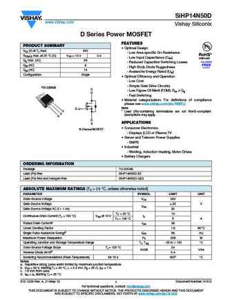
SiHP14N50D www.vishay.com Vishay Siliconix D Series Power MOSFET FEATURES PRODUCT SUMMARY Optimal Design VDS (V) at TJ max. 550 - Low Area specific On-Resistance RDS(on) max. at 25 C ( ) VGS = 10 V 0.4 - Low Input Capacitance (Ciss) Qg max. (nC) 58 - Reduced Capacitive Switching Losses Qgs (nC) 8 - High Body Diode Ruggedness Qgd (nC) 14 - Avalanche Energy Rated (UIS) Co
ixfh21n50 ixfh24n50 ixfh26n50 ixfm21n50 ixfm24n50 ixfm26n50 ixft24n50 ixft26n50.pdf
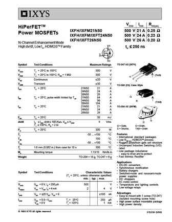
VDSS ID25 RDS(on) HiPerFETTM IXFH/IXFM21N50 500 V 21 A 0.25 Power MOSFETs IXFH/IXFM/IXFT24N50 500 V 24 A 0.23 IXFH/IXFT26N50 500 V 26 A 0.20 N-Channel Enhancement Mode High dv/dt, Low trr, HDMOSTM Family trr 250 ns TO-247 AD (IXFH) Symbol Test Conditions Maximum Ratings VDSS TJ = 25 C to
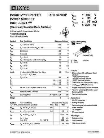
ixfk64n50p ixfx64n50p.pdf
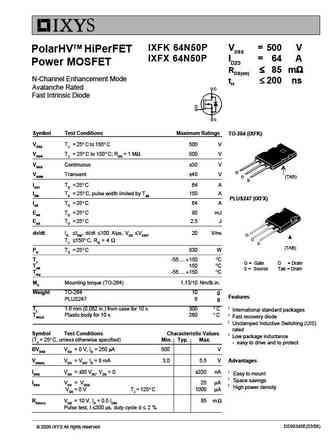
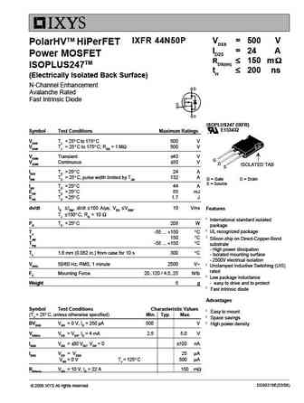
IXFK 64N50P VDSS = 500 V PolarHVTM HiPerFET IXFX 64N50P ID25 = 64 A Power MOSFET RDS(on) 85 m N-Channel Enhancement Mode trr 200 ns Avalanche Rated Fast Intrinsic Diode Symbol Test Conditions Maximum Ratings TO-264 (IXFK) VDSS TJ = 25 C to 150 C 500 V VDGR TJ = 25 C to 150 C; RGS = 1 M 500 V VGSS Continuo
ixfh24n50q ixft24n50q ixfh26n50q ixft26n50q.pdf
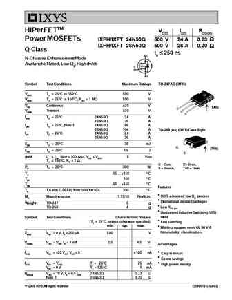
HiPerFETTM VDSS ID25 RDS(on) Power MOSFETs IXFH/IXFT 24N50Q 500 V 24 A 0.23 IXFH/IXFT 26N50Q 500 V 26 A 0.20 Q-Class trr 250 ns N-Channel Enhancement Mode Avalanche Rated, Low Qg, High dv/dt Symbol Test Conditions Maximum Ratings TO-247 AD (IXFH) VDSS TJ = 25 C to 150 C 500 V VDGR TJ = 25 C to 150 C; RGS = 1
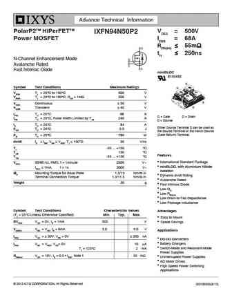
ixfk94n50p2 ixfx94n50p2.pdf
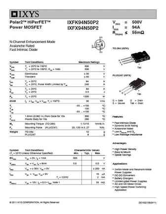
Polar2TM HiPerFETTM VDSS = 500V IXFK94N50P2 Power MOSFET ID25 = 94A IXFX94N50P2 RDS(on) 55m N-Channel Enhancement Mode Avalanche Rated TO-264 (IXFK) Fast Intrinsic Diode G Symbol Test Conditions Maximum Ratings D S VDSS TJ = 25 C to 150 C 500 V Tab VDGR TJ = 25 C to 150 C, RGS = 1M 500 V VGSS Continuous 30 V PLUS247 (IXFX) VGSM Tr
ixtq44n50p.pdf
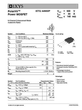
IXTQ 44N50P VDSS = 500 V PolarHVTM ID25 = 44 A Power MOSFET RDS(on) 140 m N-Channel Enhancement Mode Avalanche Rated Symbol Test Conditions Maximum Ratings TO-3P (IXTQ) VDSS TJ = 25 C to 150 C 500 V VDGR TJ = 25 C to 150 C; RGS = 1 M 500 V VGS Continuous 30 V VGSM Transient 40 V G ID25 TC = 25 C44 A D (TAB) IDM TC = 25
ixgh24n50bu1 ixgh24n60bu1.pdf
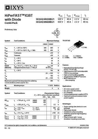
VCES IC(25) VCE(sat) tfi HiPerFASTTM IGBT 500 V 48 A 2.3 V 80 ns IXGH24N50BU1 with Diode 600 V 48 A 2.5 V 80 ns IXGH24N60BU1 Combi Pack Preliminary data TO-247 AD Symbol Test Conditions Maximum Ratings 24N50 24N60 C (TAB) VCES TJ = 25 C to 150 C 500 600 V G VCGR TJ = 25 C to 150 C; RGE = 1 M 500 600 V C E VGES Continuous 20 V VGEM Transient 30 V G = Gate, C = Collector, E
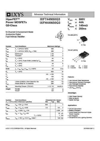
ixfr44n50q3.pdf
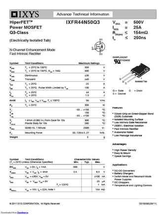
Advance Technical Information HiperFETTM VDSS = 500V IXFR44N50Q3 P wer MOSFET ID25 = 25A Q3-CIass RDS( n) 154m trr 250ns (EIectricaIIy Is Iated Tab) N-Channel Enhancement Mode Fast Intrinsic Rectifier ISOPLUS247 E153432 Symb I Test C nditi ns Maximum Ratings VDSS TJ = 25 C to 150 C 500 V VDGR TJ = 25 C to 150 C, RGS = 1M 500 V VGSS Continuous 30 V G VGSM Transient 40
ixfn44n50 ixfk44n50 ixfn48n50 ixfk48n50.pdf
VDSS ID25 RDS(on) HiPerFETTM IXFK / IXFN 44 N50 500 V 44 A 0.12 Power MOSFETs IXFK / IXFN 48 N50 500 V 48 A 0.10 trr 250 ns N-Channel Enhancement Mode Avalanche Rated, High dv/dt, Low trr TO-264 AA Symbol Test Conditions Maximum Ratings (IXFK) IXFK IXFN VDSS TJ = 25 C to 150 C 500 500 V VDGR TJ = 25 C
ixfx74n50p2 ixfk74n50p2.pdf
Advance Technical Information PolarP2TM HiPerFETTM VDSS = 500V IXFK74N50P2 Power MOSFET ID25 = 74A IXFX74N50P2 RDS(on) 77m trr 250ns N-Channel Enhancement Mode Avalanche Rated Fast Intrinsic Diode TO-264 (IXFK) Symbol Test Conditions Maximum Ratings G D VDSS TJ = 25 C to 150 C 500 V S VDGR TJ = 25 C to 150 C, RGS
ixfh44n50p ixfk44n50p ixft44n50p.pdf
IXFH 44N50P VDSS = 500 V PolarHVTM HiPerFET IXFK 44N50P ID25 = 44 A Power MOSFET IXFT 44N50P RDS(on) 140 m N-Channel Enhancement Mode trr 200 ns Avalanche Rated Fast Intrinsic Diode TO-247 AD (IXFH) Symbol Test Conditions Maximum Ratings VDSS TJ = 25 C to 175 C 500 V VDGR TJ = 25 C to 175 C; RGS = 1 M 500
ixfr24n50 ixfr26n50.pdf
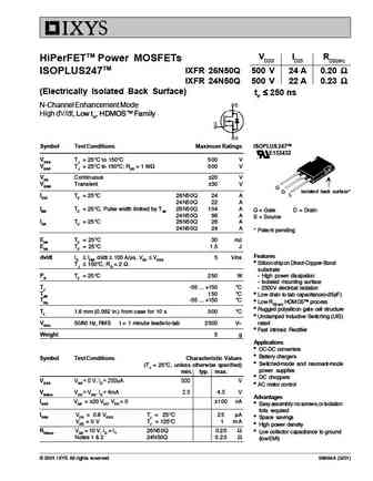
Advanced Technical Information VDSS ID25 RDS(on) HiPerFETTM Power MOSFETs IXFR 26N50 500 V 24 A 0.20 W ISOPLUS247TM IXFR 24N50 500 V 22 A 0.23 W (Electrically Isolated Back Surface) trr 250 ns N-Channel Enhancement Mode High dV/dt, Low trr, HDMOSTM Family ISOPLUS 247TM Symbol Test Conditions Maximum Ratings VDSS TJ = 25 C to 150 C 500 V VDGR TJ = 25 C to 150 C; RGS = 1 MW 50
ixfr64n50p.pdf
IXFR 64N50P VDSS = 500 V PolarHVTM HiPerFET ID25 = 35 A Power MOSFET RDS(on) 95 m ISOPLUS247TM trr 200 ns (Electrically Isolated Back Surface) N-Channel Enhancement Mode Avalanche Rated Fast Intrinsic Diode Symbol Test Conditions Maximum Ratings ISOPLUS247 (IXFR) E153432 VDSS TJ = 25 C to 150 C 500 V VDGR TJ
ixfn64n50p.pdf
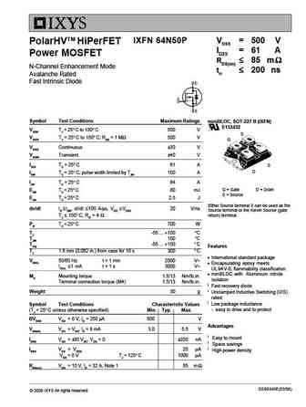
IXFN 64N50P VDSS = 500 V PolarHVTM HiPerFET ID25 = 61 A Power MOSFET RDS(on) 85 m N-Channel Enhancement Mode trr 200 ns Avalanche Rated Fast Intrinsic Diode Symbol Test Conditions Maximum Ratings miniBLOC, SOT-227 B (IXFN) E153432 VDSS TJ = 25 C to 150 C 500 V S VDGR TJ = 25 C to 150 C; RGS = 1 M 500 V G
ixtp2r4n50p ixty2r4n50p.pdf
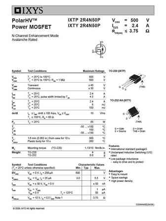
IXTP 2R4N50P VDSS = 500 V PolarHVTM IXTY 2R4N50P ID25 = 2.4 A Power MOSFET RDS(on) 3.75 N-Channel Enhancement Mode Avalanche Rated Symbol Test Conditions Maximum Ratings TO-220 (IXTP) VDSS TJ = 25 C to 150 C 500 V VDGR TJ = 25 C to 150 C; RGS = 1 M 500 V VGSM Transient 40 V (TAB) G VGSM Continuous 30 V D S ID25 TC = 25 C 2.4 A
ixfx44n50f ixfk44n50f.pdf
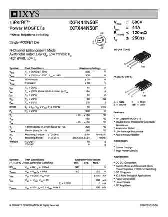
HiPerRFTM VDSS = 500V IXFK44N50F ID25 = 44A Power MOSFETs IXFX44N50F RDS(on) 120m F-Class MegaHertz Switching trr 250ns Single MOSFET Die TO-264 (IXFK) N-Channel Enhancement Mode Avalanche Rated, Low Qg, Low Intrinsic Rg High dV/dt, Low trr G D Tab S Symbol Test Conditions Maximum Ratings VDSS TJ = 25 C to 150 C
ixfk44n50 ixfn44n50 ixfk48n50 ixfn48n50.pdf

VDSS ID25 RDS(on) HiPerFETTM IXFK / IXFN 44 N50 500 V 44 A 0.12 Power MOSFETs IXFK / IXFN 48 N50 500 V 48 A 0.10 trr 250 ns N-Channel Enhancement Mode Avalanche Rated, High dv/dt, Low trr TO-264 AA Symbol Test Conditions Maximum Ratings (IXFK) IXFK IXFN VDSS TJ = 25 C to 150 C 500 500 V VDGR TJ = 25 C
ixft44n50q3.pdf

Reduce The Size of Your High Power Design 1000V Q3-Class HiPerFETTM Power MOSFET in SMPD Package Technology Q3-Class HiPerFETTM Features Low Rdson & Qg Low Intrinsic Gate Resistance Fast Intrinsic Rectifier Excellent dV/dt Performance High Avalanche Energy Capabilities SMPD Package Features High Speed Switching Capabilities Compact, Ultra-low Package Pr
ixfn44n50u2-u3 ixfn48n50u2-u3.pdf
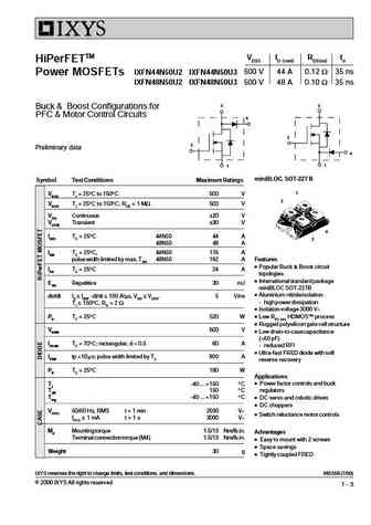
VDSS ID (cont) RDS(on) trr HiPerFETTM 500 V 44 A 0.12 W 35 ns IXFN44N50U2 IXFN44N50U3 Power MOSFETs IXFN48N50U2 IXFN48N50U3 500 V 48 A 0.10 W 35 ns 3 3 Buck & Boost Configurations for PFC & Motor Control Circuits 4 2 2 Preliminary data 4 1 1 miniBLOC, SOT-227 B Symbol Test Conditions Maximum Ratings 1 VDSS TJ = 25 C to 150 C 500 V 2 VDGR TJ = 25 C to 150 C; RGS = 1 MW 5
ixfh34n50p3 ixfq34n50p3.pdf
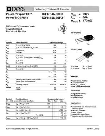
Preliminary Technical Information Polar3TM HiperFETTM VDSS = 500V IXFQ34N50P3 ID25 = 34A Power MOSFETs IXFH34N50P3 RDS(on) 170m N-Channel Enhancement Mode Avalanche Rated Fast Intrinsic Rectifier TO-3P (IXFQ) G D Symbol Test Conditions Maximum Ratings S Tab VDSS TJ = 25 C to 150 C 500 V VDGR TJ = 25 C to 150 C, RGS = 1M 500 V TO-247
ixfr24n50q ixfr26n50q.pdf
VDSS ID25 RDS(on) HiPerFETTM Power MOSFETs IXFR 26N50Q 500 V 24 A 0.20 ISOPLUS247TM IXFR 24N50Q 500 V 22 A 0.23 (Electrically Isolated Back Surface) trr 250 ns N-Channel Enhancement Mode High dV/dt, Low t , HDMOSTM Family rr Symbol Test Conditions Maximum Ratings ISOPLUS 247TM E153432 VDSS TJ = 25 C to 150 C
ixfk48n50q ixfx48n50q ixfk44n50q ixfx44n50q.pdf
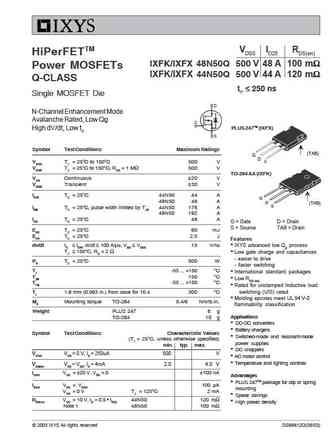
VDSS ID25 RDS(on) HiPerFETTM IXFK/IXFX 48N50Q 500 V 48 A 100 m Power MOSFETs IXFK/IXFX 44N50Q 500 V 44 A 120 m Q-CLASS trr 250 ns Single MOSFET Die N-Channel Enhancement Mode Avalanche Rated, Low Qg PLUS 247TM (IXFX) High dV/dt, Low trr Symbol Test Conditions Maximum Ratings (TAB) G D VDSS TJ = 25 C to 150
ixgh24n50b ixgh24n60b.pdf
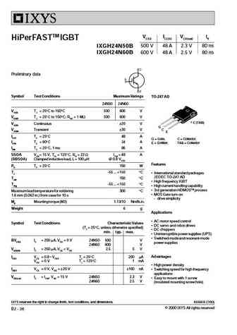
VCES IC(25) VCE(sat) tfi HiPerFASTTM IGBT IXGH24N50B 500 V 48 A 2.3 V 80 ns 600 V 48 A 2.5 V 80 ns IXGH24N60B Preliminary data Symbol Test Conditions Maximum Ratings TO-247 AD 24N50 24N60 VCES TJ = 25 C to 150 C 500 600 V VCGR TJ = 25 C to 150 C; RGE = 1 M 500 600 V C (TAB) VGES Continuous 20 V G VGEM Transient 30 V C E IC25 TC = 25 C48 A G = Gate, C = Collector, IC90 TC = 9
ixfh44n50q3.pdf
Advance Technical Information HiperFETTM V = 500V IXFT44N50Q3 DSS Power MOSFETs ID25 = 44A IXFH44N50Q3 Q3-Class RDS(on) 140m trr 250ns N-Channel Enhancement Mode Avalanche Rated TO-268 (IXFT) Fast Intrinsic Rectifier G S D (Tab) Symbol Test Conditions Maximum Ratings VDSS TJ = 25 C to 150 C 500 V TO-247 (IXFH) VDG
ixth21n50 ixth24n50 ixtm21n50 ixtm24n50.pdf
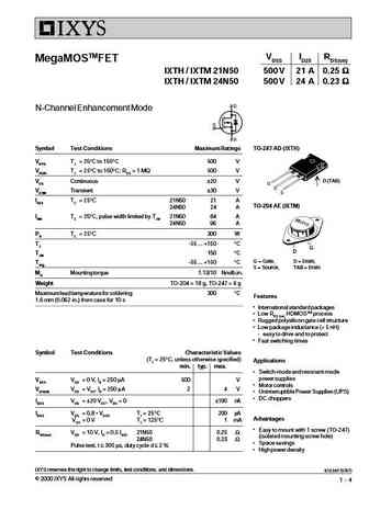
VDSS ID25 RDS(on) MegaMOSTMFET IXTH / IXTM 21N50 500 V 21 A 0.25 IXTH / IXTM 24N50 500 V 24 A 0.23 N-Channel Enhancement Mode Symbol Test Conditions Maximum Ratings TO-247 AD (IXTH) VDSS TJ = 25 C to 150 C 500 V VDGR TJ = 25 C to 150 C; RGS = 1 M 500 V D (TAB) VGS Continuous 20 V VGSM Transient 30 V ID25 TC = 25 C 21N50 21 A
ixfn94n50p2.pdf
Advance Technical Information PolarP2TM HiPerFETTM VDSS = 500V IXFN94N50P2 Power MOSFET ID25 = 68A RDS(on) 55m trr 250ns N-Channel Enhancement Mode Avalanche Rated Fast Intrinsic Diode miniBLOC E153432 S Symbol Test Conditions Maximum Ratings G VDSS TJ = 25 C to 150 C 500 V VDGR TJ = 25 C to 150 C, RGS = 1
mtw14n50e.pdf
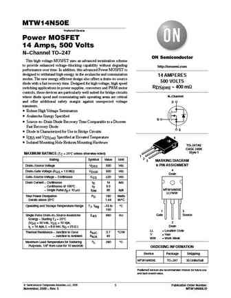
MTW14N50E Preferred Device Power MOSFET 14 Amps, 500 Volts N Channel TO 247 This high voltage MOSFET uses an advanced termination scheme to provide enhanced voltage blocking capability without degrading http //onsemi.com performance over time. In addition, this advanced Power MOSFET is designed to withstand high energy in the avalanche and commutation 14 AMPERES modes. The new
ndd04n50z.pdf
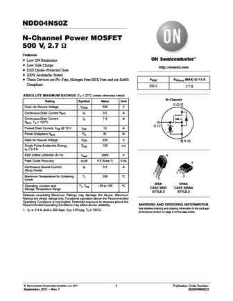
NDD04N50Z N-Channel Power MOSFET 500 V, 2.7 W Features Low ON Resistance Low Gate Charge http //onsemi.com ESD Diode-Protected Gate 100% Avalanche Tested VDSS RDS(on) (MAX) @ 1.5 A These Devices are Pb-Free, Halogen Free/BFR Free and are RoHS Compliant 500 V 2.7 W ABSOLUTE MAXIMUM RATINGS (TC = 25 C unless otherwise noted) N-Channel Rating Symbol Value Unit
fda24n50f.pdf

Is Now Part of To learn more about ON Semiconductor, please visit our website at www.onsemi.com Please note As part of the Fairchild Semiconductor integration, some of the Fairchild orderable part numbers will need to change in order to meet ON Semiconductor s system requirements. Since the ON Semiconductor product management systems do not have the ability to manage part nomenclatur
14n50.pdf
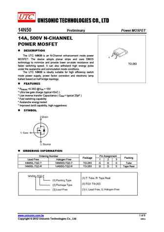
UNISONIC TECHNOLOGIES CO., LTD 14N50 Preliminary Power MOSFET 14A, 500V N-CHANNEL POWER MOSFET DESCRIPTION The UTC 14N50 is an N-Channel enhancement mode power 1 MOSFET. The device adopts planar stripe and uses DMOS technology to minimize and provide lower on-state resistance and TO-263 faster switching speed. It can also withstand high energy pulse under the avalanche and
24n50.pdf
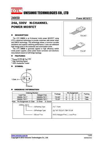
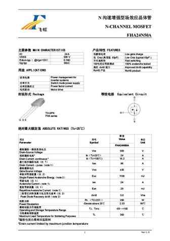
UNISONIC TECHNOLOGIES CO., LTD 24N50 Power MOSFET 24A, 500V N-CHANNEL POWER MOSFET DESCRIPTION The UTC 24N50 is an N-channel mode power MOSFET using UTC s advanced technology to provide customers with planar stripe and DMOS technology. This technology allows a minimum on-state resistance and superior switching performance. It also can withstand high energy pulse in the aval
14n50l-tf1-t 14n50g-tf1-t 14n50l-tf3-t 14n50g-tf3-t 14n50l-t3p-t 14n50g-t3p-t.pdf
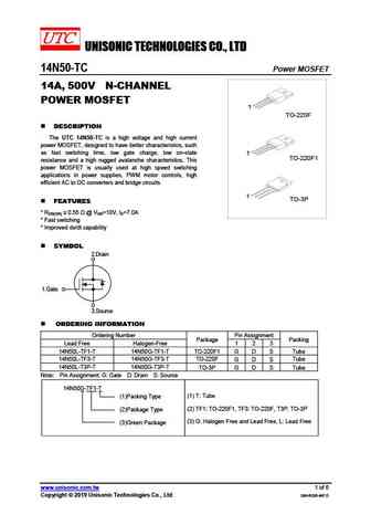
UNISONIC TECHNOLOGIES CO., LTD 14N50-TC Power MOSFET 14A, 500V N-CHANNEL POWER MOSFET 1 TO-220F DESCRIPTION The UTC 14N50-TC is a high voltage and high current power MOSFET, designed to have better characteristics, such as fast switching time, low gate charge, low on-state 1 TO-220F1 resistance and a high rugged avalanche characteristics. This power MOSFET is usually u
14n50l-ta3-t 14n50g-ta3-t 14n50l-tf1-t 14n50g-tf1-t 14n50l-tq2-t 14n50g-tq2-t 14n50l-tq2-r 14n50g-tq2-r.pdf

UNISONIC TECHNOLOGIES CO., LTD 14N50 Power MOSFET 14A, 500V N-CHANNEL POWER MOSFET DESCRIPTION The UTC 14N50 is a N-Channel enhancement mode power MOSFET. The device adopts planar stripe and uses DMOS technology to minimize and provide lower on-state resistance and faster switching speed. It can also withstand high energy pulse under the avalanche and commutation mode cond
24n50a.pdf
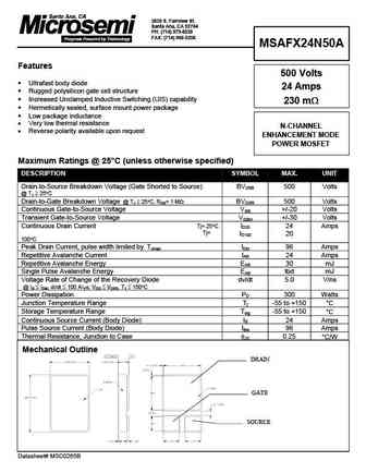
2830 S. Fairview St. Santa Ana, CA 92704 PH (714) 979-8220 FAX (714) 966-5256 MSAFX24N50A Features 500 Volts Ultrafast body diode 24 Amps Rugged polysilicon gate cell structure Increased Unclamped Inductive Switching (UIS) capability 230 m Hermetically sealed, surface mount power package Low package inductance Very low thermal resistance N-CHANNE
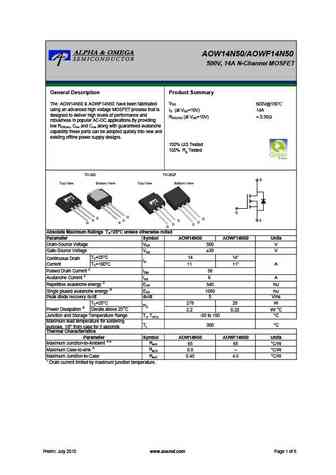
aowf14n50.pdf
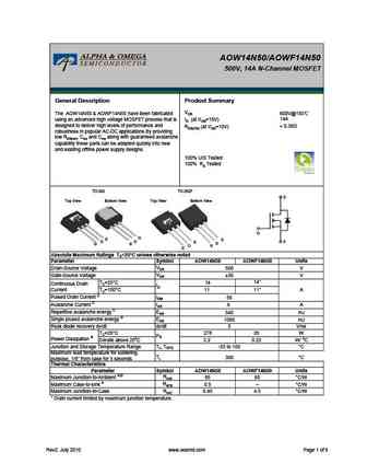
AOW14N50/AOWF14N50 500V, 14A N-Channel MOSFET General Description Product Summary VDS The AOW14N50 & AOWF14N50 have been fabricated 600V@150 using an advanced high voltage MOSFET process that is 14A ID (at VGS=10V) designed to deliver high levels of performance and
aob14n50.pdf
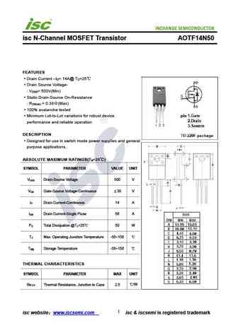
AOT14N50/AOB14N50/AOTF14N50 500V, 14A N-Channel MOSFET General Description Product Summary VDS 600V@150 The AOT14N50 &AOB14N50 & AOTF14N50 have been fabricated using an advanced high voltage MOSFET ID (at VGS=10V) 14A process that is designed to deliver high levels of RDS(ON) (at VGS=10V)
aot14n50.pdf

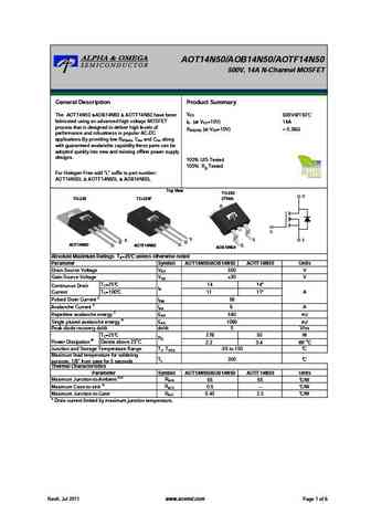
AOT14N50/AOB14N50/AOTF14N50 500V, 14A N-Channel MOSFET General Description Product Summary VDS 600V@150 The AOT14N50 &AOB14N50 & AOTF14N50 have been fabricated using an advanced high voltage MOSFET ID (at VGS=10V) 14A process that is designed to deliver high levels of RDS(ON) (at VGS=10V)
aotf14n50fd.pdf

AOT14N50FD/AOTF14N50FD 500V, 14A N-Channel MOSFET General Description Product Summary VDS 600V@150 The AOT14N50FD/AOTF14N50FD have been fabricated using an advanced high voltage MOSFET process that is ID (at VGS=10V) 14A designed to deliver high levels of performance and RDS(ON) (at VGS=10V)
aot14n50fd.pdf
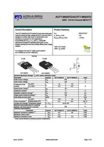
AOT14N50FD/AOTF14N50FD 500V, 14A N-Channel MOSFET General Description Product Summary VDS 600V@150 The AOT14N50FD/AOTF14N50FD have been fabricated using an advanced high voltage MOSFET process that is ID (at VGS=10V) 14A designed to deliver high levels of performance and RDS(ON) (at VGS=10V)
aotf14n50.pdf

AOT14N50/AOB14N50/AOTF14N50 500V, 14A N-Channel MOSFET General Description Product Summary VDS 600V@150 The AOT14N50 &AOB14N50 & AOTF14N50 have been fabricated using an advanced high voltage MOSFET ID (at VGS=10V) 14A process that is designed to deliver high levels of RDS(ON) (at VGS=10V)
aot14n50 aotf14n50.pdf
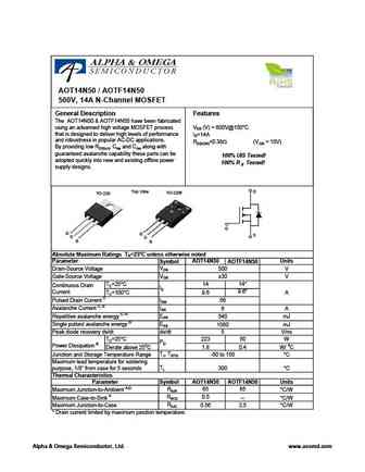
AOT14N50 / AOTF14N50 500V, 14A N-Channel MOSFET General Description Features The AOT14N50 & AOTF14N50 have been fabricated using an advanced high voltage MOSFET process VDS (V) = 600V@150 C that is designed to deliver high levels of performance ID=14A and robustness in popular AC-DC applications. RDS(ON)
aow14n50 aowf14n50.pdf
AOW14N50/AOWF14N50 500V, 14A N-Channel MOSFET General Description Product Summary VDS 600V@150 The AOW14N50 & AOWF14N50 have been fabricated using an advanced high voltage MOSFET process that is ID (at VGS=10V) 14A designed to deliver high levels of performance and RDS(ON) (at VGS=10V)
aow14n50.pdf

AOW14N50/AOWF14N50 500V, 14A N-Channel MOSFET General Description Product Summary VDS The AOW14N50 & AOWF14N50 have been fabricated 600V@150 using an advanced high voltage MOSFET process that is 14A ID (at VGS=10V) designed to deliver high levels of performance and
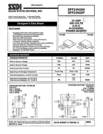
sff44n50s1 sff44n50s2.pdf
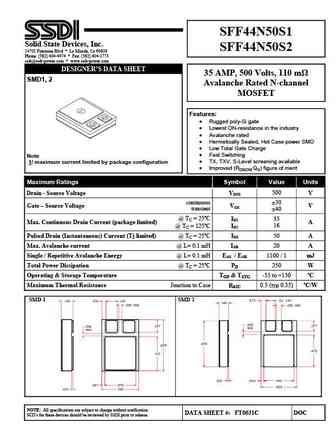
SFF44N50S1 Solid State Devices, Inc. SFF44N50S2 14701 Firestone Blvd * La Mirada, Ca 90638 Phone (562) 404-4474 * Fax (562) 404-1773 ssdi@ssdi-power.com * www.ssdi-power.com DESIGNER S DATA SHEET 35 AMP, 500 Volts, 110 m SMD1, 2 Avalanche Rated N-channel MOSFET Features Rugged poly-Si gate Lowest ON-resistance in the industry Avalanche rated
sff44n50m sff44n50z.pdf

SFF44N50M Solid State Devices, Inc. SFF44N50Z 14701 Firestone Blvd * La Mirada, Ca 90638 Phone (562) 404-4474 * Fax (562) 404-1773 ssdi@ssdi-power.com * www.ssdi-power.com DESIGNER S DATA SHEET 25 AMP , 500 Volts, 110 m Avalanche Rated N-channel TO-254 TO-254Z MOSFET Features Rugged poly-Si gate Lowest ON-resistance in the industry Avalanche rated
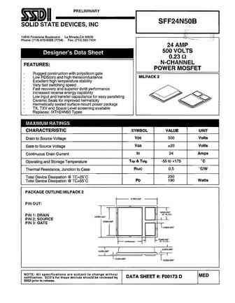
sff24n50.pdf
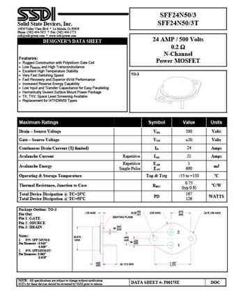
SFF24N50/3 SFF24N50/3T Solid State Devices, Inc. 14830 Valley View Blvd * La Mirada, Ca 90638 Phone (562) 404-7855 * Fax (562) 404-1773 ssdi@ssdi-power.com * www.ssdi-power.com 24 AMP / 500 Volts DESIGNER S DATA SHEET 0.2 N-Channel Features Power MOSFET Rugged Construction with Polysilicon Gate Cell Low R and High Transconductance DS(ON) Excellent H
mp4n50fr.pdf
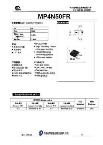
N R N-CHANNEL MOSFET MP4N50FR Package MAIN CHARACTERISTICS ID 4A VDSS 500V Rdson-max 2.8 Vgs=10V Qg-Typ 7.4nC APPLICATIONS High efficiency switch mode power supplies Variable frequency LED household appliance LED power supp
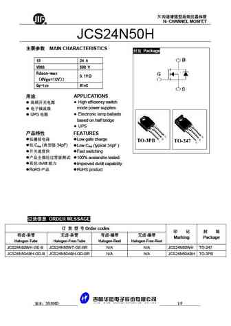
jcs24n50wh jcs24n50abh.pdf
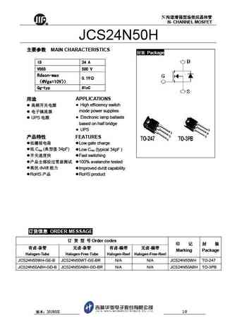
N N- CHANNEL MOSFET R JCS24N50H MAIN CHARACTERISTICS Package ID 24 A VDSS 500 V Rdson-max 0.19 @Vgs=10V Qg-typ 81nC APPLICATIONS High efficiency switch mode power supplies Electronic lamp ballasts UPS based on half bridge
fta14n50c ftp14n50c.pdf
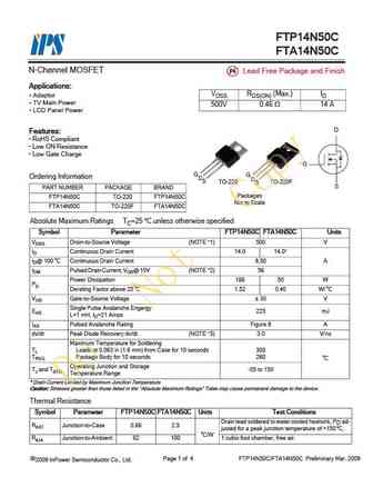
FTP14N50C FTA14N50C N-Channel MOSFET Pb Lead Free Package and Finish Applications VDSS RDS(ON) (Max.) ID Adaptor TV Main Power 500V 0.46 14 A LCD Panel Power D Features RoHS Compliant Low ON Resistance Low Gate Charge G G G Ordering Information DS DS TO-220F TO-220 S PART NUMBER PACKAGE BRAND Packages FTP14N50C TO-220 FTP14N50C Not to Sc
bru24n50.pdf
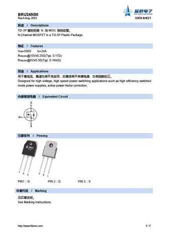
BRU24N50 Rev.A Aug.-2023 DATA SHEET / Descriptions TO-3P N MOS N-Channel MOSFET in a TO-3P Plastic Package. / Features V =500V I =24A DS D R DS(ON)@10V 0.25 (Typ. 0.17 ) R DS(ON)@6V 0.3 (Typ. 0.18m ) / Applications
24n50b 24n50c.pdf
RoHS 24N50 Series RoHS SEMICONDUCTOR Nell High Power Products N-Channel Power MOSFET 24A, 500Volts DESCRIPTION D The Nell 24N50 is a three-terminal silicon device with current conduction capability of 24A, fast switching speed, low on-state resistance, breakdown voltage rating of 500V, and max. threshold voltage of 4 volts. They are designed for use in applications such as G
cs24n50 anhd.pdf
Silicon N-Channel Power MOSFET R CS24N50 ANHD General Description VDSS 500 V CS24N50 ANHD, the silicon N-channel Enhanced ID 24 A PD(TC=25 ) 230 W VDMOSFETs, is obtained by the self-aligned planar Technology RDS(ON)Typ 0.18 which reduce the conduction loss, improve switching performance and enhance the avalanche energy. The transistor can be used in various
cs24n50.pdf
CS24N50 N PD TC=25 300 W 0.40 W/ ID VGS=10V,TC=25 24 A IDM 96 VGS 20 V Tjm +150 Tstg -55 +150 RthJC 0.42 /W BVDSS VGS=0V,ID=0.25mA 500 V RDS on VGS=10V,ID=12A 0.23 VGS th VDS=VGS,ID=4mA 2.
kqb4n50.pdf
SMD Type IC SMD Type IC SMD Type Transistors SMD Type Transistors SMDType SMDType IC Product specification KQB4N50 TO-263 Unit mm 4.57+0.2 -0.2 Features +0.1 1.27-0.1 3.4A, 500 V. RDS(ON) =2.7 @VGS =10V Low gate charge (typical 10nC) Low Crss(typical 6.0pF) +0.1 Fast switching 0.1max 1.27-0.1 100% avalanche tested 0.81+0.1 -0.1 lmproved dv/dt capability 2.54 1gate 1Ga
wfw24n50n.pdf
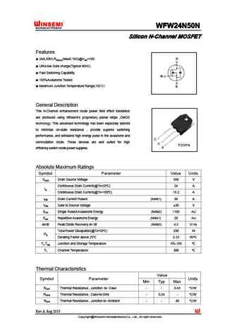
WFW24N50N WFW24N50N WFW24N50N WFW24N50N Silicon N-Channel MOSFET Silicon N-Channel MOSFET Silicon N-Channel MOSFET Silicon N-Channel MOSFET Features 24A,500V,RDS(on)(Max0.19 )@VGS=10V Ultra-low Gate charge(Typical 90nC) Fast Switching Capability 100%Avalanche Tested Maximum Junction Temperature Range(150 ) General Description This N-Channel enhancement mod
wfw24n50w.pdf
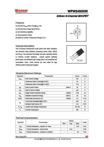
WFW24N50W WFW24N50W WFW24N50W WFW24N50W Silicon N-Channel MOSFET Silicon N-Channel MOSFET Silicon N-Channel MOSFET Silicon N-Channel MOSFET Features 24A,500V,RDS(on)(Max0.19 )@VGS=10V Ultra-low Gate charge(Typical 90nC) Fast Switching Capability 100%Avalanche Tested Maximum Junction Temperature Range(150 ) General Description This N-Channel enhancement mod
cmt14n50.pdf
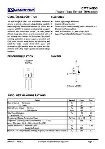
CMT14N50 POWER FIELD EFFECT TRANSISTOR GENERAL DESCRIPTION FEATURES This high voltage MOSFET uses an advanced termination Robust High Voltage Termination scheme to provide enhanced voltage-blocking capability Avalanche Energy Specified without degrading performance over time. In addition, this Source-to-Drain Diode Recovery Time Comparable to a advanced MOSFET is designed to w
ctm14n50.pdf
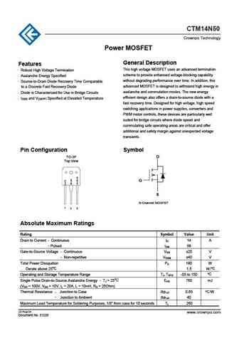
CTM14N50 Crownpo Technology Power MOSFET General Description Features . This high voltage MOSFET uses an advanced termination Robust High Voltage Termination . scheme to provide enhanced voltage-blocking capability Avalanche Energy Specified . without degrading performance over time. In addition, this Source-to-Drain Diode Recovery Time Comparable advanced MOSFET is designed to wit
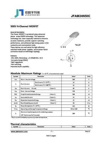
jfam24n50c.pdf
JFAM24N50C 500V N-Channel MOSFET General Description This Power MOSFET is produced using advanced planar stripe DMOS technology. This advanced technology has been especially tailored to minimize on-state resistance, provide superior switching performance, and withstand high energy pulse in the avalanche and commutation mode. These devices are well suited for high efficiency
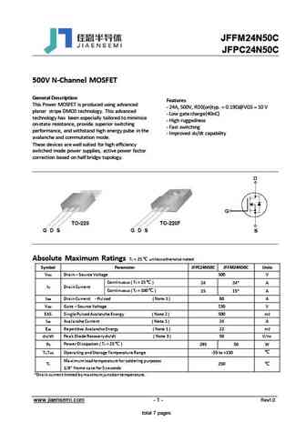
jfpc24n50c jffm24n50c.pdf
JFFM24N50C JFPC24N50C 500V N-Channel MOSFET General Description Features This Power MOSFET is produced using advanced - 24A, 500V, RDS(on)typ. = 0.19 @VGS = 10 V planar stripe DMOS technology. This advanced - Low gate charge(40nC) technology has been especially tailored to minimize - High ruggedness on-state resistance, provide superior switching - Fast switching perf
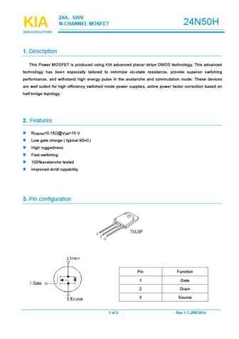
kia24n50h.pdf
24A 500V 24N50H N-CHANNELMOSFET KIA KIA KIA SEMICONDUCTORS SEMICONDUCTORS SEMICONDUCTORS 1.Description This Power MOSFET is produced using KIAadvanced planar stripe DMOS technology. This advanced technology has been especially tailored to minimize on-state resistance, provide superior switching performance, and withstand high energy pulse in the avalanche and commutation mode. The
slw24n50c.pdf
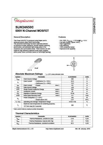
SLW24N50C 500V N-Channel MOSFET General Description Features This Power MOSFET is produced using Maple semi s - 25A, 500V, RDS(on)typ. = 167m @VGS = 10 V advanced planar stripe DMOS technology. - Low gate charge ( typical 96nC) This advanced technology has been especially tailored - High ruggedness to minimize on-state resistance, provide superior switching - Fast switching performanc
slw24n50c slh24n50c.pdf
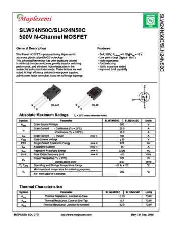
LEAD FREE Pb RoHS SLW24N50C/SLH24N50C 500V N-Channel MOSFET General Description Features This Power MOSFET is produced using Maple semi s - 24A, 500V, RDS(on) = 0.2 @VGS = 10 V advanced planar stripe DMOS technology. - Low gate charge ( typical 96nC) This advanced technology has been especially tailored - High ruggedness to minimize on-state resistance, provide superior switching -
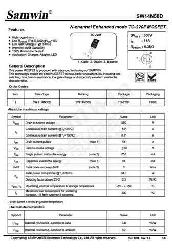
swf14n50d.pdf
SW14N50D N-channel Enhanced mode TO-220F MOSFET Features TO-220F BVDSS 500V High ruggedness Low RDS(ON) (Typ 0.38 )@VGS=10V ID 14A Low Gate Charge (Typ 54nC) RDS(ON) 0.38 Improved dv/dt Capability 100% Avalanche Tested 2 1 Application Charger, Adaptor, LED 2 3 1 1. Gate 2. Drain 3. Source General Description 3 This power MOSFET is produce
swn4n50k swd4n50k swf4n50k.pdf
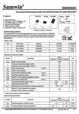
SW4N50K N-channel Enhanced mode TO-251N/TO-252/TO-220F MOSFET Features TO-251N TO-252 TO-220F BVDSS 500V ID 4A High ruggedness Low RDS(ON) (Typ 0.76 )@VGS=10V RDS(ON) 0.76 Low Gate Charge (Typ 13nC) Improved dv/dt Capability 100% Avalanche Tested 1 1 1 2 2 2 2 Application Charger, Adaptor, LED 3 3 3 1. Gate 2. Drain 3. S
swt24n50d.pdf
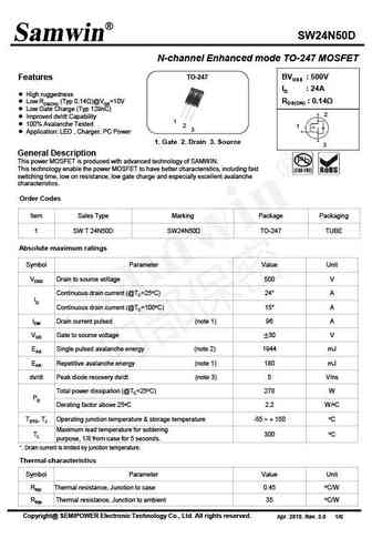
SW24N50D N-channel Enhanced mode TO-247 MOSFET TO-247 BVDSS 500V Features ID 24A High ruggedness RDS(ON) 0.14 Low RDS(ON) (Typ 0.14 )@VGS=10V Low Gate Charge (Typ 129nC) 2 Improved dv/dt Capability 1 100% Avalanche Tested 2 1 3 Application LED , Charger, PC Power 1. Gate 2. Drain 3. Source 3 General Description This p
hfa24n50g.pdf
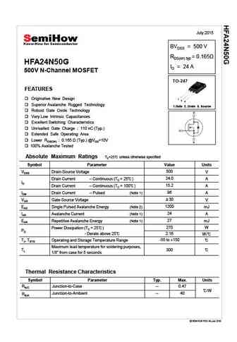
July 2015 BVDSS = 500 V RDS(on) typ HFA24N50G ID = 24 A 500V N-Channel MOSFET TO-247 FEATURES Originative New Design 1 2 3 Superior Avalanche Rugged Technology 1.Gate 2. Drain 3. Source Robust Gate Oxide Technology Very Low Intrinsic Capacitances Excellent Switching Characteristics Unrivalled Gate Charge 110 nC (Typ.) Extended Safe Operating Area Lo
hfd4n50.pdf
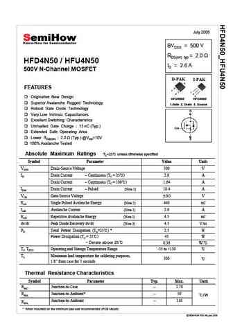
July 2005 BVDSS = 500 V RDS(on) typ HFD4N50 / HFU4N50 ID = 2.6 A 500V N-Channel MOSFET D-PAK I-PAK 2 FEATURES 1 1 3 2 3 Originative New Design HFD4N50 HFU4N50 Superior Avalanche Rugged Technology 1.Gate 2. Drain 3. Source Robust Gate Oxide Technology Very Low Intrinsic Capacitances Excellent Switching Characteristics Unrivalled Gate Charge 13 nC (Typ.
hfp4n50.pdf
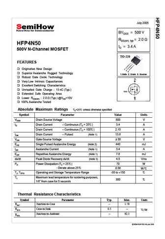
July 2005 BVDSS = 500 V RDS(on) typ HFP4N50 ID = 3.4 A 500V N-Channel MOSFET TO-220 FEATURES Originative New Design 1 2 3 Superior Avalanche Rugged Technology 1.Gate 2. Drain 3. Source Robust Gate Oxide Technology Very Low Intrinsic Capacitances Excellent Switching Characteristics Unrivalled Gate Charge 13 nC (Typ.) Extended Safe Operating Area Lower RDS(ON
hfs4n50.pdf
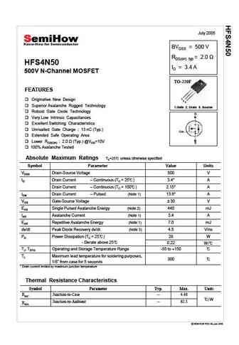
July 2005 BVDSS = 500 V RDS(on) typ HFS4N50 ID = 3.4 A 500V N-Channel MOSFET TO-220F FEATURES 1 Originative New Design 2 3 Superior Avalanche Rugged Technology 1.Gate 2. Drain 3. Source Robust Gate Oxide Technology Very Low Intrinsic Capacitances Excellent Switching Characteristics Unrivalled Gate Charge 13 nC (Typ.) Extended Safe Operating Area Lo
hfd4n50 hfu4n50.pdf

July 2005 BVDSS = 500 V RDS(on) typ HFD4N50 / HFU4N50 ID = 2.6 A 500V N-Channel MOSFET D-PAK I-PAK 2 FEATURES 1 1 3 2 3 Originative New Design HFD4N50 HFU4N50 Superior Avalanche Rugged Technology 1.Gate 2. Drain 3. Source Robust Gate Oxide Technology Very Low Intrinsic Capacitances Excellent Switching Characteristics Unrivalled Gate Charge 13 nC (Typ.
wvm4n50.pdf
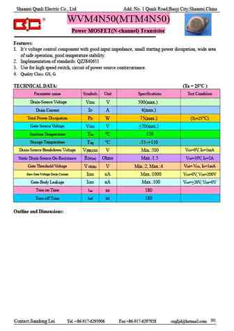
Shaanxi Qunli Electric Co., Ltd Add. No. 1 Qunli Road,Baoji City,Shaanxi,China WVM4N50(MTM4N50) Power MOSFET(N-channel) Transistor Features 1. It s voltage control component with good input impedance, small starting power dissipation, wide area of safe operation, good temperature stability. 2. Implementation of standards QZJ840611 3. Use for high speed switch, circuit of power
smos44n50 smos48n50.pdf
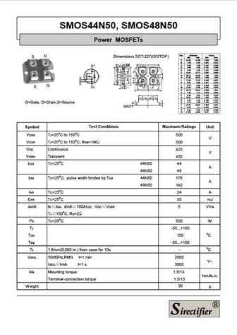
SMOS44N50, SMOS48N50 Power MOSFETs Dim. Millimeter Inches D Dimensions SOT-227(ISOTOP) S Min. Max. Min. Max. A 31.50 31.88 1.240 1.255 B 7.80 8.20 0.307 0.323 C 4.09 4.29 0.161 0.169 D 4.09 4.29 0.161 0.169 E 4.09 4.29 0.161 0.169 F 14.91 15.11 0.587 0.595 G 30.12 30.30 1.186 1.193 H 37.80 38.20 1.489 1.505 J 11.68 12.22 0.460 0.481 K 8.92 9.60 0.351 0.378 L 0.76 0.84 0.030 0.0
smos44n50d2 smos44n50d3.pdf
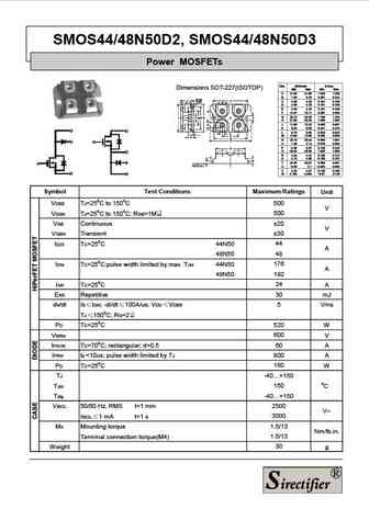
SMOS44/48N50D2, SMOS44/48N50D3 Power MOSFETs Dim. Millimeter Inches Dimensions SOT-227(ISOTOP) Min. Max. Min. Max. A 31.50 31.88 1.240 1.255 B 7.80 8.20 0.307 0.323 C 4.09 4.29 0.161 0.169 D 4.09 4.29 0.161 0.169 E 4.09 4.29 0.161 0.169 F 14.91 15.11 0.587 0.595 G 30.12 30.30 1.186 1.193 H 37.80 38.20 1.489 1.505 J 11.68 12.22 0.460 0.481 K 8.92 9.60 0.351 0.378 L 0.76 0.84 0.030
tsa24n50m.pdf
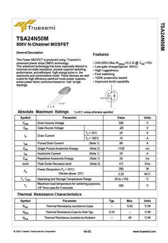
TSA24N50M 500V N-Channel MOSFET General Description Features This Power MOSFET is produced using Truesemi s 24A,500V,Max.RDS(on)=0.2 @ VGS =10V advanced planar stripe DMOS technology. This advanced technology has been especially tailored to Low gate charge(typical 90nC) minimize on-state resistance, provide superior switching High ruggedness performance, and
wm04n50m.pdf
WM04N50M N-Channel Enhancement MOSFET Features Way-on Small Signal MOSFETs V = 40V, I = 5A DS D R
fir14n50fg.pdf
FIR14N50FG CREAT BY ART Advanced N-Ch Power MOSFET-G PIN Connection TO-220F VDSS 500 V ID 13 A PD (TC=25 ) 150 W RDS(ON) 0.4 G D S Features Fast Switching g Schematic dia ram Low ON Resistance(Rdson 0.5 ) D Low Gate Charge (Typical Data 85nC) Low Reverse transfer capacitances(Typical 100pF) G 100% Single Pulse avalanche energy Test S Marking Di
fir24n50aptg.pdf
FIR24N50APTG High Voltage N-Channel MOSFET PIN Connection TO-3P Features Low Intrinsic Capacitances Excellent Switching Characteristics Extended Safe Operating Area Unrivalled Gate Charge 90 nC (Typ.) g Schematic dia ram BVDSS=500V,ID=24A D Lower RDS(on) 0.2 (Max) @VG=10V G 100% Avalanche Tested S Marking Diagram Y = Year A = Assembly Location
spa24n50g.pdf
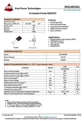
SPA24N50G Sinai Power Technologies www.sinai-power.com N-channel Power MOSFET PRODUCT SUMMARY Features V (V) at T max. 500 DS J ID=24A(Vgs=10V) R max. at 25oC ( ) V =10V 0.2 DS(on) GS Ultra Low Gate Charge Q max. (nC) 160 g Improved dv/dt Capability Q (nC) 30 gs 100% Avalanche Tested Q (nC) 53 gd ROHS compliant Configuration single A
hm24n50a.pdf
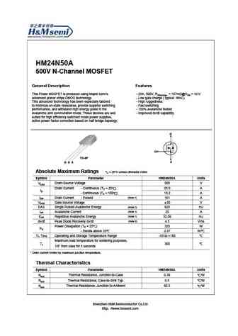
HM24N50A 500V N-Channel MOSFET General Description Features This Power MOSFET is produced using Maple semi s - 25A, 500V, RDS(on)typ. = 167m @VGS = 10 V advanced planar stripe DMOS technology. - Low gate charge ( typical 96nC) This advanced technology has been especially tailored - High ruggedness to minimize on-state resistance, provide superior switching - Fast switching performance
ixfh44n50p.pdf
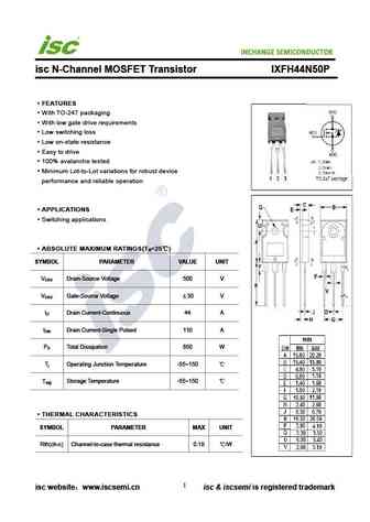
INCHANGE Semiconductor isc N-Channel MOSFET Transistor IXFH44N50P FEATURES With TO-247 packaging With low gate drive requirements Low switching loss Low on-state resistance Easy to drive 100% avalanche tested Minimum Lot-to-Lot variations for robust device performance and reliable operation APPLICATIONS Switching applications ABSOLUTE MAXIMUM RATINGS(T =25 )
ixfx64n50q3.pdf
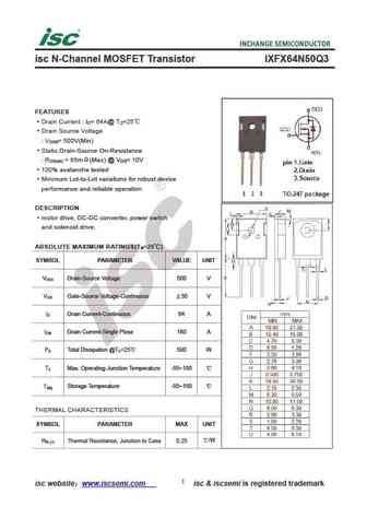
isc N-Channel MOSFET Transistor IXFX64N50Q3 FEATURES Drain Current I = 64A@ T =25 D C Drain Source Voltage V = 500V(Min) DSS Static Drain-Source On-Resistance R = 85m (Max) @ V = 10V DS(on) GS 100% avalanche tested Minimum Lot-to-Lot variations for robust device performance and reliable operation DESCRIPTION motor drive, DC-DC converter, power switch and sol
aob14n50.pdf
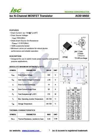
isc N-Channel MOSFET Transistor AOB14N50 FEATURES Drain Current I = 14A@ T =25 D C Drain Source Voltage- V = 500V(Min) DSS Static Drain-Source On-Resistance R = 0.38 (Max) DS(on) 100% avalanche tested Minimum Lot-to-Lot variations for robust device performance and reliable operation DESCRIPTION Designed for use in switch mode power supplies and general purp
aot14n50.pdf
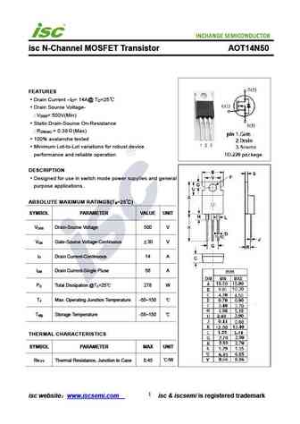
isc N-Channel MOSFET Transistor AOT14N50 FEATURES Drain Current I = 14A@ T =25 D C Drain Source Voltage- V = 500V(Min) DSS Static Drain-Source On-Resistance R = 0.38 (Max) DS(on) 100% avalanche tested Minimum Lot-to-Lot variations for robust device performance and reliable operation DESCRIPTION Designed for use in switch mode power supplies and general purp
aotf14n50fd.pdf
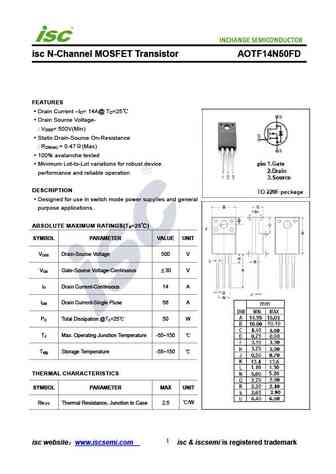
isc N-Channel MOSFET Transistor AOTF14N50FD FEATURES Drain Current I = 14A@ T =25 D C Drain Source Voltage- V = 500V(Min) DSS Static Drain-Source On-Resistance R = 0.47 (Max) DS(on) 100% avalanche tested Minimum Lot-to-Lot variations for robust device performance and reliable operation DESCRIPTION Designed for use in switch mode power supplies and general p
ixtm24n50.pdf
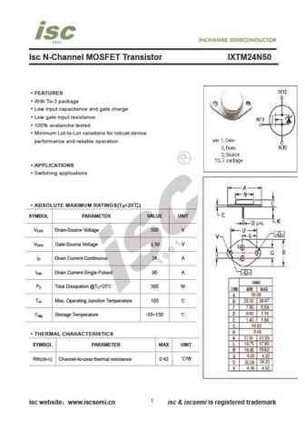
Isc N-Channel MOSFET Transistor IXTM24N50 FEATURES With To-3 package Low input capacitance and gate charge Low gate input resistance 100% avalanche tested Minimum Lot-to-Lot variations for robust device performance and reliable operation APPLICATIONS Switching applications ABSOLUTE MAXIMUM RATINGS(T =25 ) a SYMBOL PARAMETER VALUE UNIT V Drain-Source Voltage 500
aot14n50fd.pdf

isc N-Channel MOSFET Transistor AOT14N50FD FEATURES Drain Current I = 14A@ T =25 D C Drain Source Voltage- V = 500V(Min) DSS Static Drain-Source On-Resistance R = 0.47 (Max) DS(on) 100% avalanche tested Minimum Lot-to-Lot variations for robust device performance and reliable operation DESCRIPTION Designed for use in switch mode power supplies and general pu
aotf14n50.pdf
isc N-Channel MOSFET Transistor AOTF14N50 FEATURES Drain Current I = 14A@ T =25 D C Drain Source Voltage- V = 500V(Min) DSS Static Drain-Source On-Resistance R = 0.38 (Max) DS(on) 100% avalanche tested Minimum Lot-to-Lot variations for robust device performance and reliable operation DESCRIPTION Designed for use in switch mode power supplies and general pur
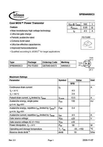
spp04n50c3.pdf
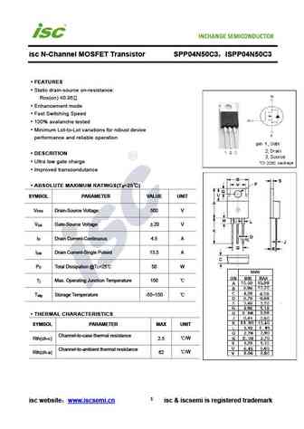
isc N-Channel MOSFET Transistor SPP04N50C3 ISPP04N50C3 FEATURES Static drain-source on-resistance RDS(on) 0.95 Enhancement mode Fast Switching Speed 100% avalanche tested Minimum Lot-to-Lot variations for robust device performance and reliable operation DESCRITION Ultra low gate charge Improved transcondutance ABSOLUTE MAXIMUM RATINGS(T =25 ) a SYMBO
spd04n50c3.pdf
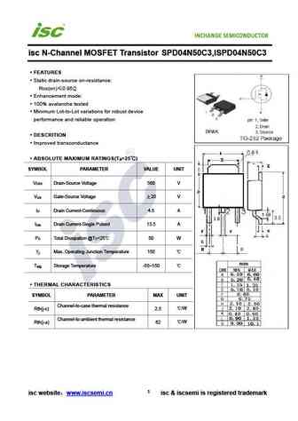
isc N-Channel MOSFET Transistor SPD04N50C3,ISPD04N50C3 FEATURES Static drain-source on-resistance RDS(on) 0.95 Enhancement mode 100% avalanche tested Minimum Lot-to-Lot variations for robust device performance and reliable operation DESCRITION Improved transconductance ABSOLUTE MAXIMUM RATINGS(T =25 ) a SYMBOL PARAMETER VALUE UNIT V Drain-Source Voltage 560
fqa24n50f.pdf
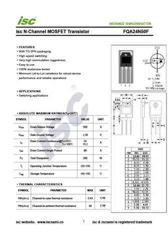
INCHANGE Semiconductor isc N-Channel MOSFET Transistor FQA24N50F FEATURES With TO-3PN packaging High speed switching Very high commutation ruggedness Easy to use 100% avalanche tested Minimum Lot-to-Lot variations for robust device performance and reliable operationz APPLICATIONS Switching applications ABSOLUTE MAXIMUM RATINGS(T =25 ) a SYMBOL PARAMETER VALUE
fdh44n50.pdf
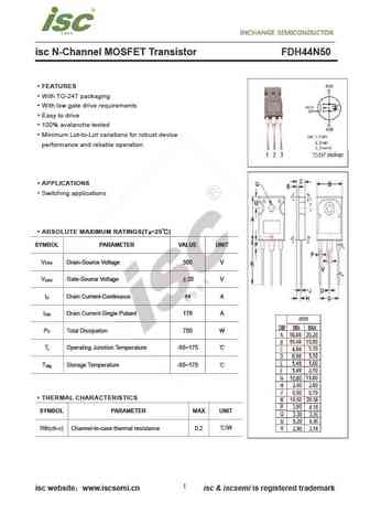
isc N-Channel MOSFET Transistor FDH44N50 FEATURES With TO-247 packaging With low gate drive requirements Easy to drive 100% avalanche tested Minimum Lot-to-Lot variations for robust device performance and reliable operation APPLICATIONS Switching applications ABSOLUTE MAXIMUM RATINGS(T =25 ) a SYMBOL PARAMETER VALUE UNIT V Drain-Source Voltage 500 V DSS V Gate
fda24n50f.pdf
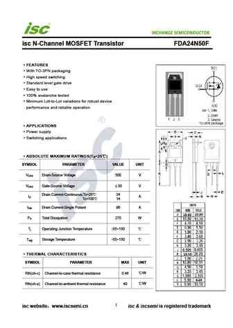
INCHANGE Semiconductor isc N-Channel MOSFET Transistor FDA24N50F FEATURES With TO-3PN packaging High speed switching Standard level gate drive Easy to use 100% avalanche tested Minimum Lot-to-Lot variations for robust device performance and reliable operation APPLICATIONS Power supply Switching applications ABSOLUTE MAXIMUM RATINGS(T =25 ) a SYMBOL PARAMET
fda44n50.pdf
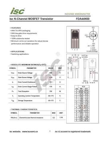
isc N-Channel MOSFET Transistor FDA44N50 FEATURES With TO-3PN packaging With low gate drive requirements Easy to drive 100% avalanche tested Minimum Lot-to-Lot variations for robust device performance and reliable operation APPLICATIONS Switching applications ABSOLUTE MAXIMUM RATINGS(T =25 ) a SYMBOL PARAMETER VALUE UNIT V Drain-Source Voltage 500 V DSS V Gate
aow14n50.pdf
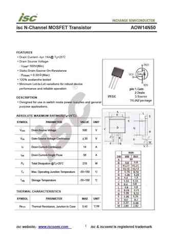
isc N-Channel MOSFET Transistor AOW14N50 FEATURES Drain Current I = 14A@ T =25 D C Drain Source Voltage- V = 500V(Min) DSS Static Drain-Source On-Resistance R = 0.38 (Max) DS(on) 100% avalanche tested Minimum Lot-to-Lot variations for robust device performance and reliable operation DESCRIPTION Designed for use in switch mode power supplies and general purp
Другие IGBT... UK3568, UF450, UF460, 1N50, 1N50Z, 2N50, 3N50, 3N50Z, 13N50, 5N50, 5N50K, 6N50, 7N50, 8N50, 1N40, 2N40, 3N40
Параметры MOSFET. Взаимосвязь и компромиссы
🌐 : EN ES РУ

Список транзисторов
Обновления
MOSFET: CEZC2P07 | CEZ2R05 | CEU3133 | CES2361 | CES2312A | CEP100N10L | CEM3425 | CEM3139 | CEM3133 | CEM3115 | CED3133 | CEC3257 | CEC2533 | CEB100N10L | BC3134KT | BC3134K
Popular searches
2sb754 | 2sc2362 | 2sd468 | c2240 transistor | 2sc1918 | c1213 transistor | 2sc1400 replacement | 2sb817