6N50 datasheet, аналоги, основные параметры
Наименование производителя: 6N50 📄📄
Тип транзистора: MOSFET
Полярность: N
Предельные значения
Pd ⓘ - Максимальная рассеиваемая мощность: 89 W
|Vds|ⓘ - Максимально допустимое напряжение сток-исток: 500 V
|Vgs|ⓘ - Максимально допустимое напряжение затвор-исток: 30 V
|Id| ⓘ - Максимально допустимый постоянный ток стока: 6 A
Tj ⓘ - Максимальная температура канала: 150 °C
Электрические характеристики
tr ⓘ - Время нарастания: 30 ns
Cossⓘ - Выходная емкость: 85 pf
RDSonⓘ - Сопротивление сток-исток открытого транзистора: 0.95 Ohm
📄📄 Копировать
Аналог (замена) для 6N50
- подборⓘ MOSFET транзистора по параметрам
6N50 даташит
6n50.pdf
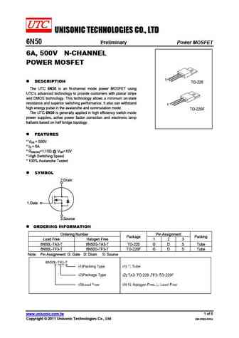
UNISONIC TECHNOLOGIES CO., LTD 6N50 Preliminary Power MOSFET 6A, 500V N-CHANNEL POWER MOSFET 1 DESCRIPTION TO-220 The UTC 6N50 is an N-channel mode power MOSFET using UTC s advanced technology to provide customers with planar stripe and DMOS technology. This technology allows a minimum on-state resistance and superior switching performance. It also can withstand 1 high e
ste24n90 ste36n50-da ste36n50-dk ste38n60 ste38na50 ste45n50 ste50n40 ste90n25.pdf
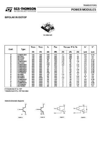
TRANSISTORS POWER MODULES BIPOLAR IN ISOTOP For other conf. VCEO VCEV IC Ptot VCE (sat) @IC / IB ts* tf* Conf. Type (V) (V) (A) (W) (V) (A) (A) ( s) ( s) D ESM2012DV 125 150 120 175 2 100 1 0.9 0.15 A BUT30V 125 200 100 250 1.5 100 10 1.0 0.1 B BUT230V 125 200 200 300 1.9 200 20 1.0 0.1 A BUT32V 300 400 80 250 1.9 40 4 1.9 0.12 D ESM2030DV 300 400 67 150 2.2 56 1.6 2.0 0.35 B BUT2
ste26n50.pdf
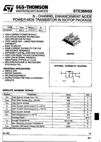
STE26N50 N - CHANNEL ENHANCEMENT MODE POWER MOS TRANSISTOR IN ISOTOP PACKAGE TYPE V R I DSS DS(on) D STE26N50 500 V
hgtp6n40e1d hgtp6n50e1d.pdf
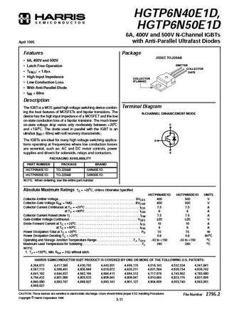
HGTP6N40E1D, S E M I C O N D U C T O R HGTP6N50E1D 6A, 400V and 500V N-Channel IGBTs with Anti-Parallel Ultrafast Diodes April 1995 Features Package JEDEC TO-220AB 6A, 400V and 500V EMITTER Latch Free Operation COLLECTOR TFALL
ste36n50a.pdf
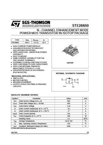
STE36N50A N - CHANNEL ENHANCEMENT MODE POWER MOS TRANSISTOR IN ISOTOP PACKAGE TYPE V R I DSS DS(on) D STE36N50A 500 V
hgtd6n40e1 hgtd6n40e1s hgtd6n50e1 hgtd6n50e1s.pdf
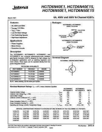
HGTD6N40E1, HGTD6N40E1S, HGTD6N50E1, HGTD6N50E1S 6A, 400V and 500V N-Channel IGBTs March 1997 Features Packages HGTD6N40E1, HGTD6N50E1 6A, 400V and 500V JEDEC TO-251AA VCE(ON) 2.5V Max. EMITTER COLLECTOR TFALL 1.0 s GATE Low On-State Voltage Fast Switching Speeds COLLECTOR (FLANGE) High Input Impedance HGTD6N40E1S, HGTD6N50E1S Applications JEDEC TO
mtv16n50e.pdf
MOTOROLA Order this document SEMICONDUCTOR TECHNICAL DATA by MTV16N50E/D Advance Information MTV16N50E TMOS E-FET. Power Field Effect Transistor D3PAK for Surface Mount TMOS POWER FET N Channel Enhancement Mode Silicon Gate 16 AMPERES 500 VOLTS This high voltage MOSFET uses an advanced termination RDS(on) = 0.40 OHM scheme to provide enhanced voltage blocking capability
irfb16n50kpbf.pdf
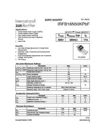
PD - 95619 SMPS MOSFET IRFB16N50KPbF Applications l Switch Mode Power Supply (SMPS) HEXFET Power MOSFET l Uninterruptible Power Supply l High Speed Power Switching VDSS RDS(on) typ. ID l Hard Switched and High Frequency Circuits 500V 285m 17A l Lead-Free Benefits l Low Gate Charge Qg results in Simple Drive Requirement l Improved Gate, Avalanche and Dynamicdv/dt S D Ruggedne
php6n50e phb6n50e.pdf
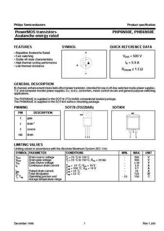
Philips Semiconductors Product specification PowerMOS transistors PHP6N50E, PHB6N50E Avalanche energy rated FEATURES SYMBOL QUICK REFERENCE DATA d Repetitive Avalanche Rated Fast switching VDSS = 500 V Stable off-state characteristics High thermal cycling performance ID = 5.9 A g Low thermal resistance RDS(ON) 1.5 s GENERAL DESCRIPTION N-channel, enh
std16n50m2 stf16n50m2 stp16n50m2.pdf
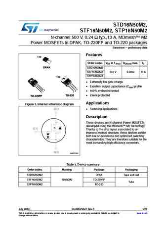
STD16N50M2, STF16N50M2, STP16N50M2 N-channel 500 V, 0.24 typ.,13 A, MDmesh M2 Power MOSFETs in DPAK, TO-220FP and TO-220 packages Datasheet - preliminary data Features TAB 3 Order codes VDS @ TJmax RDS(on) max. ID 1 DPAK STD16N50M2 STF16N50M2 550 V 0.28 13 A STP16N50M2 TAB Extremely low gate charge Excellent output capacitance (Coss) profile 3 3 2 2 10
stf16n50u.pdf
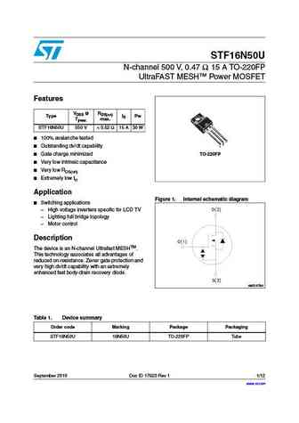
STF16N50U N-channel 500 V, 0.47 , 15 A TO-220FP UltraFAST MESH Power MOSFET Features VDSS @ RDS(on) Type ID Pw Tjmax. max. STF16N50U 550 V
fqp6n50c.pdf
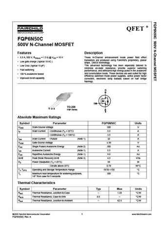
QFET FQP6N50C 500V N-Channel MOSFET Features Description 5.5 A, 500 V, RDS(on) = 1.2 @ VGS = 10 V These N-Channel enhancement mode power field effect transistors are produced using Fairchild s proprietary, planar Low gate charge ( typical 19 nC ) stripe, DMOS technology. This advanced technology has been especially tailored to Low Crss ( typical 15 pF) minimize
fda16n50.pdf
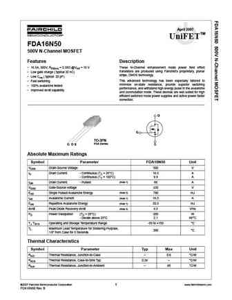
April 2007 TM UniFET FDA16N50 500V N-Channel MOSFET Features Description 16.5A, 500V, RDS(on) = 0.38 @VGS = 10 V These N-Channel enhancement mode power field effect transistors are produced using Fairchild s proprietary, planar Low gate charge ( typical 32 nC) stripe, DMOS technology. Low Crss ( typical 20 pF) This advanced technology has been especially tailored to
fdpf16n50 fdpf16n50t.pdf
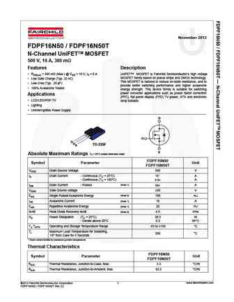
November 2013 FDPF16N50 / FDPF16N50T N-Channel UniFETTM MOSFET 500 V, 16 A, 380 m Features Description RDS(on) = 380 m (Max.) @ VGS = 10 V, ID = 8 A UniFETTM MOSFET is Fairchild Semiconductor s high voltage MOSFET family based on planar stripe and DMOS technology. Low Gate Charge (Typ. 32 nC) This MOSFET is tailored to reduce on-state resistance, and to Low Crss (
fda16n50ldtu.pdf
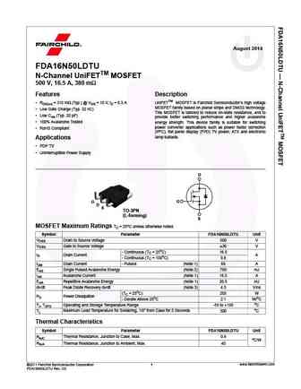
August 2014 FDA16N50LDTU N-Channel UniFETTM MOSFET 500 V, 16.5 A, 380 m Features Description RDS(on) = 310 m (Typ.) @ VGS = 10 V, ID = 8.3 A UniFETTM MOSFET is Fairchild Semiconductor s high voltage MOSFET family based on planar stripe and DMOS technology. Low Gate Charge (Typ. 32 nC) This MOSFET is tailored to reduce on-state resistance, and to Low Crss (Typ. 20 pF)
fdp16n50u fdpf16n50ut.pdf
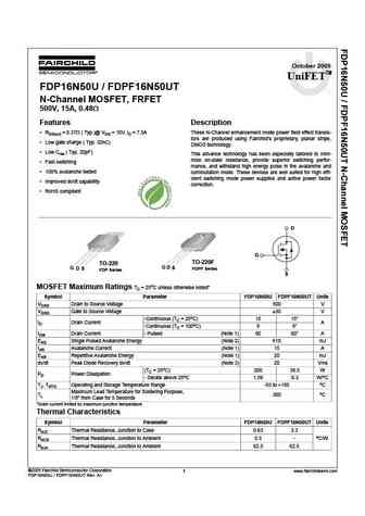
October 2009 UniFETTM FDP16N50U / FDPF16N50UT tm N-Channel MOSFET, FRFET 500V, 15A, 0.48 Features Description RDS(on) = 0.37 ( Typ.)@ VGS = 10V, ID = 7.5A These N-Channel enhancement mode power field effect transis- tors are produced using Fairchild s proprietary, planar stripe, Low gate charge ( Typ. 32nC) DMOS technology. Low Crss ( Typ. 20pF) This advance tech
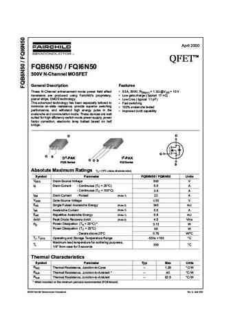
fqd6n50ctf fqd6n50ctm fqd6n50c fqu6n50c.pdf
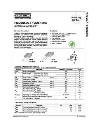
October 2008 QFET FQD6N50C / FQU6N50C 500V N-Channel MOSFET General Description Features These N-Channel enhancement mode power field effect 4.5A, 500V, RDS(on) = 1.2 @VGS = 10 V transistors are produced using Fairchild s proprietary, Low gate charge (typical 19nC) planar stripe, DMOS technology. Low Crss (typical 15pF) This advanced technology has been especially t
fda16n50 f109.pdf
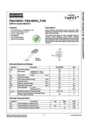
July 2007 TM UniFET FDA16N50 / FDA16N50_F109 500V N-Channel MOSFET Features Description 16.5A, 500V, RDS(on) = 0.38 @VGS = 10 V These N-Channel enhancement mode power field effect transistors are produced using Fairchild s proprietary, planar Low gate charge ( typical 32 nC) stripe, DMOS technology. Low Crss ( typical 20 pF) This advanced technology has been especial
fqp6n50.pdf
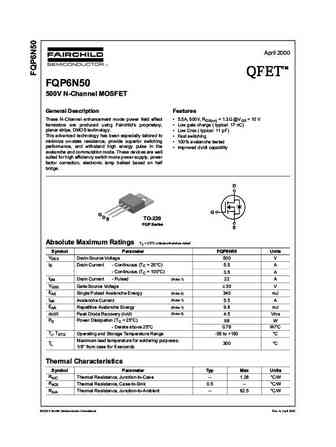
April 2000 TM QFET QFET QFET QFET 500V N-ChanneI MOSFET GeneraI Description Features These N-Channel enhancement mode power field effect 5.5A, 500V, RDS(on) = 1.3 @VGS = 10 V transistors are produced using Fairchild s proprietary, Low gate charge ( typical 17 nC) planar stripe, DMOS technology. Low Crss ( typical 11 pF) This advanced technology has been e
fqpf6n50.pdf

April 2000 TM QFET QFET QFET QFET 500V N-ChanneI MOSFET GeneraI Description Features These N-Channel enhancement mode power field effect 3.6A, 500V, RDS(on) = 1.3 @VGS = 10 V transistors are produced using Fairchild s proprietary, Low gate charge ( typical 17 nC) planar stripe, DMOS technology. Low Crss ( typical 11 pF) This advanced technology has been
fdp16n50.pdf
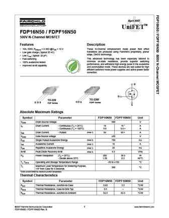
April 2007 TM UniFET FDP16N50 / FDPF16N50 500V N-Channel MOSFET Features Description 16A, 500V, RDS(on) = 0.38 @VGS = 10 V These N-Channel enhancement mode power field effect transistors are produced using Fairchild s proprietary, planar Low gate charge ( typical 32 nC) stripe, DMOS technology. Low Crss ( typical 20 pF) This advanced technology has been especially t
fdu6n50f.pdf
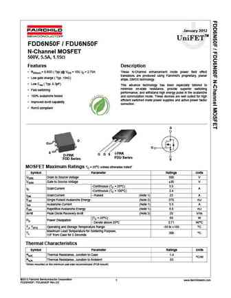
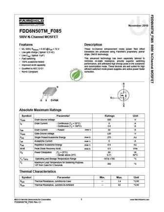
January 2012 UniFET TM FDD6N50F / FDU6N50F tm N-Channel MOSFET 500V, 5.5A, 1.15 Features Description RDS(on) = 0.95 ( Typ.)@ VGS = 10V, ID = 2.75A These N-Channel enhancement mode power field effect transistors are produced using Fairchild s proprietary, planar Low gate charge ( Typ. 15nC) stripe, DMOS technology. Low Crss ( Typ. 6.3pF) This advance technology h
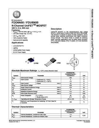
fdd6n50tf fdd6n50tm fdu6n50 fdu6n50tu.pdf
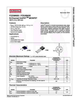
November 2013 FDD6N50 / FDU6N50 N-Channel UniFETTM MOSFET 500 V, 6 A, 900 m Features Description RDS(on) = 900 m (Max.) @ VGS = 10 V, ID = 3 A UniFETTM MOSFET is Fairchild Semiconductor s high voltage MOSFET family based on planar stripe and DMOS technology. Low Gate Charge (Typ. 12.8 nC) This MOSFET is tailored to reduce on-state resistance, and to Low Crss (Typ. 9 p
fdd6n50 fdu6n50.pdf
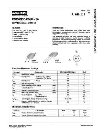
January 2006 TM UniFET FDD6N50/FDU6N50 500V N-Channel MOSFET Features Description 6A, 500V, RDS(on) = 0.9 @VGS = 10 V These N-Channel enhancement mode power field effect transistors are produced using Fairchild s proprietary, planar Low gate charge ( typical 12.8 nC) stripe, DMOS technology. Low Crss ( typical 9 pF) This advanced technology has been especially tai
fqaf16n50.pdf
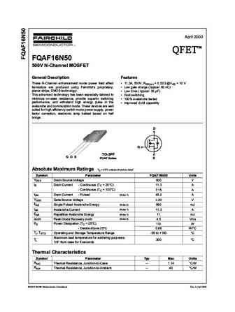
April 2000 TM QFET QFET QFET QFET 500V N-ChanneI MOSFET GeneraI Description Features These N-Channel enhancement mode power field effect 11.3A, 500V, RDS(on) = 0.32 @VGS = 10 V transistors are produced using Fairchild s proprietary, Low gate charge ( typical 60 nC) planar stripe, DMOS technology. Low Crss ( typical 35 pF) This advanced technology has be
fqa16n50.pdf
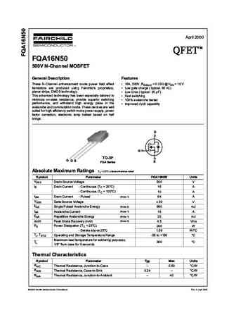
April 2000 TM QFET QFET QFET QFET 500V N-ChanneI MOSFET GeneraI Description Features These N-Channel enhancement mode power field effect 16A, 500V, RDS(on) = 0.32 @VGS = 10 V transistors are produced using Fairchild s proprietary, Low gate charge ( typical 60 nC) planar stripe, DMOS technology. Low Crss ( typical 35 pF) This advanced technology has been
fdd6n50f fdu6n50f.pdf
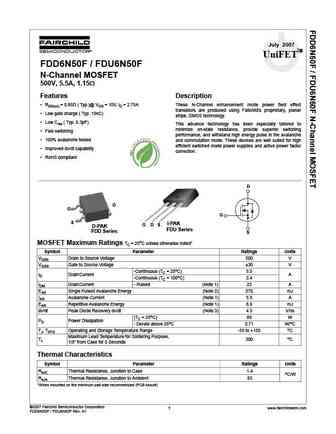
July 2007 UniFETTM FDD6N50F / FDU6N50F tm N-Channel MOSFET 500V, 5.5A, 1.15 Features Description RDS(on) = 0.95 ( Typ.)@ VGS = 10V, ID = 2.75A These N-Channel enhancement mode power field effect transistors are produced using Failchild s proprietary, planar Low gate charge ( Typ. 15nC) stripe, DMOS technology. Low Crss ( Typ. 6.3pF) This advance technology has
fdp16n50 fdpf16n50.pdf

April 2007 TM UniFET FDP16N50 / FDPF16N50 500V N-Channel MOSFET Features Description 16A, 500V, RDS(on) = 0.38 @VGS = 10 V These N-Channel enhancement mode power field effect transistors are produced using Fairchild s proprietary, planar Low gate charge ( typical 32 nC) stripe, DMOS technology. Low Crss ( typical 20 pF) This advanced technology has been especially t
fqb6n50 fqi6n50tu.pdf
April 2000 TM QFET QFET QFET QFET FQB6N50 / FQI6N50 500V N-ChanneI MOSFET GeneraI Description Features These N-Channel enhancement mode power field effect 5.5A, 500V, RDS(on) = 1.3 @VGS = 10 V transistors are produced using Fairchild s proprietary, Low gate charge ( typical 17 nC) planar stripe, DMOS technology. Low Crss ( typical 11 pF) This advanced technology
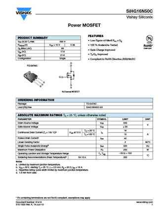
sihp16n50c sihb16n50c sihf16n50c.pdf

SiHP16N50C, SiHB16N50C, SiHF16N50C www.vishay.com Vishay Siliconix Power MOSFET FEATURES PRODUCT SUMMARY Low Figure-of-Merit Ron x Qg VDS (V) at TJ max. 560 RDS(on) ( )VGS = 10 V 0.38 100 % Avalanche Tested Qg (Max.) (nC) 68 Gate Charge Improved Qgs (nC) 17.6 Trr/Qrr Improved Qgd (nC) 21.8 Configuration Single Compliant to RoHS Directive 2002/95/EC TO-220A
sihs36n50d.pdf
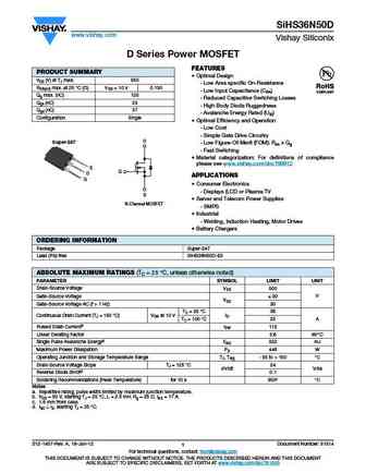
SiHS36N50D www.vishay.com Vishay Siliconix D Series Power MOSFET FEATURES PRODUCT SUMMARY Optimal Design VDS (V) at TJ max. 550 - Low Area specific On-Resistance RDS(on) max. at 25 C ( ) VGS = 10 V 0.130 - Low Input Capacitance (Ciss) Qg max. (nC) 125 - Reduced Capacitive Switching Losses Qgs (nC) 23 - High Body Diode Ruggedness Qgd (nC) 37 - Avalanche Energy Rated (UIS)
irfb16n50k irfb16n50kpbf.pdf
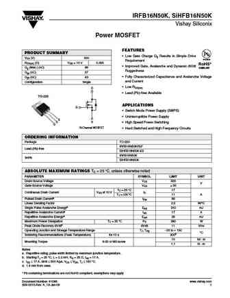
IRFB16N50K, SiHFB16N50K Vishay Siliconix Power MOSFET FEATURES PRODUCT SUMMARY Low Gate Charge Qg Results in Simple Drive VDS (V) 500 Available Requirement RDS(on) ( )VGS = 10 V 0.285 RoHS* Improved Gate, Avalanche and Dynamic dV/dt Qg (Max.) (nC) 89 COMPLIANT Ruggedness Qgs (nC) 27 Fully Characterized Capacitance and Avalanche Voltage Qgd (nC) 43 and Current Con
sihg16n50c.pdf
SiHG16N50C Vishay Siliconix Power MOSFET FEATURES PRODUCT SUMMARY Low Figure-of-Merit Ron x Qg VDS (V) at TJ max. 560 V RDS(on) ( )VGS = 10 V 0.38 100 % Avalanche Tested Qg (Max.) (nC) 68 Gate Charge Improved Qgs (nC) 17.6 Trr/Qrr Improved Qgd (nC) 21.8 Configuration Single Compliant to RoHS Directive 2002/95/EC D TO-247AC G S D G S N-Channel MOSFET
sihb16n50c sihf16n50c sihp16n50c.pdf
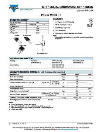
SiHP16N50C, SiHB16N50C, SiHF16N50C www.vishay.com Vishay Siliconix Power MOSFET FEATURES PRODUCT SUMMARY Low Figure-of-Merit Ron x Qg VDS (V) at TJ max. 560 RDS(on) ( )VGS = 10 V 0.38 100 % Avalanche Tested Qg (Max.) (nC) 68 Gate Charge Improved Qgs (nC) 17.6 Trr/Qrr Improved Qgd (nC) 21.8 Configuration Single Compliant to RoHS Directive 2002/95/EC TO-220A
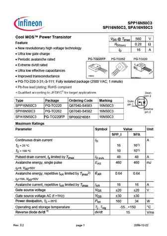
spp16n50c3 spi16n50c3 spa16n50c3 spp16n50c3 spi16n50c3 spa16n50c3 rev.3.2.pdf
spb16n50c3.pdf
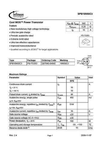
SPB16N50C3 Cool MOS Power Transistor VDS @ Tjmax 560 V Feature RDS(on) 0.28 New revolutionary high voltage technology ID 16 A Ultra low gate charge PG-TO263 Periodic avalanche rated Extreme dv/dt rated Ultra low effective capacitances Improved transconductance Type Package Ordering Code Marking SPB16N50C3 PG-TO263 Q67040-S4642 16N50C3 Maximum Rating
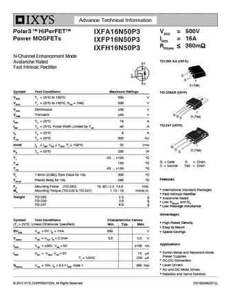
ixfh21n50 ixfh24n50 ixfh26n50 ixfm21n50 ixfm24n50 ixfm26n50 ixft24n50 ixft26n50.pdf
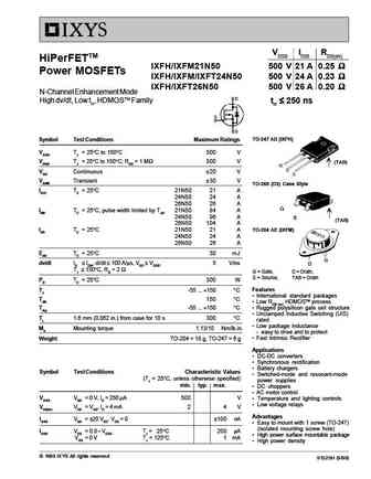
VDSS ID25 RDS(on) HiPerFETTM IXFH/IXFM21N50 500 V 21 A 0.25 Power MOSFETs IXFH/IXFM/IXFT24N50 500 V 24 A 0.23 IXFH/IXFT26N50 500 V 26 A 0.20 N-Channel Enhancement Mode High dv/dt, Low trr, HDMOSTM Family trr 250 ns TO-247 AD (IXFH) Symbol Test Conditions Maximum Ratings VDSS TJ = 25 C to
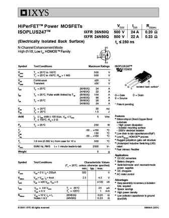
ixfc36n50p ixfr36n50p.pdf
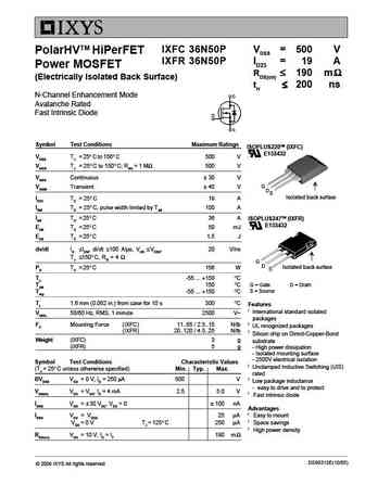
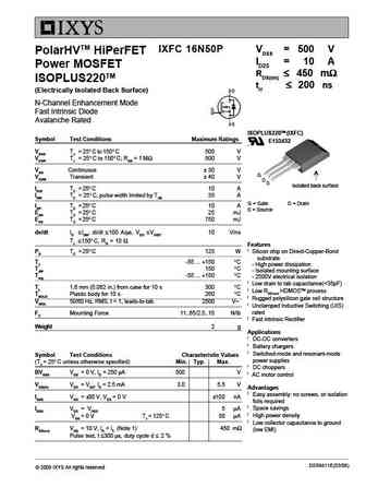
IXFC 36N50P VDSS = 500 V PolarHVTM HiPerFET IXFR 36N50P ID25 = 19 A Power MOSFET RDS(on) 190 m (Electrically Isolated Back Surface) trr 200 ns N-Channel Enhancement Mode Avalanche Rated Fast Intrinsic Diode Symbol Test Conditions Maximum Ratings ISOPLUS220TM (IXFC) E153432 VDSS TJ = 25 C to 150 C 500 V VDGR TJ
ixfh24n50q ixft24n50q ixfh26n50q ixft26n50q.pdf
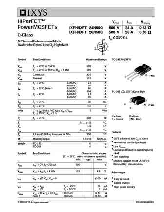
HiPerFETTM VDSS ID25 RDS(on) Power MOSFETs IXFH/IXFT 24N50Q 500 V 24 A 0.23 IXFH/IXFT 26N50Q 500 V 26 A 0.20 Q-Class trr 250 ns N-Channel Enhancement Mode Avalanche Rated, Low Qg, High dv/dt Symbol Test Conditions Maximum Ratings TO-247 AD (IXFH) VDSS TJ = 25 C to 150 C 500 V VDGR TJ = 25 C to 150 C; RGS = 1
ixta6n50d2 ixtp6n50d2 ixth6n50d2.pdf
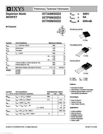
Preliminary Technical Information Depletion Mode VDSX = 500V IXTA6N50D2 MOSFET ID(on) > 6A IXTP6N50D2 RDS(on) 500m IXTH6N50D2 N-Channel TO-263 AA (IXTA) G S D (Tab) Symbol Test Conditions Maximum Ratings TO-220AB (IXTP) VDSX TJ = 25 C to 150 C 500 V VGSX Continuous 20 V VGSM Transient 30 V PD TC = 25 C 300 W G D D (Tab) TJ - 55 .
ixth16n50d2 ixtt16n50d2.pdf
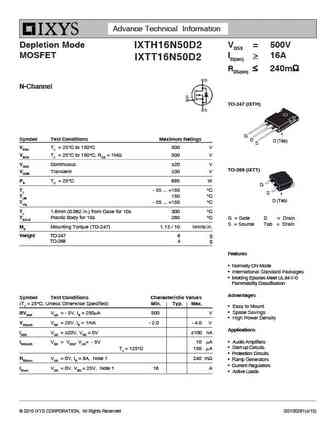
Advance Technical Information Depletion Mode VDSX = 500V IXTH16N50D2 MOSFET ID(on) > 16A IXTT16N50D2 RDS(on) 240m N-Channel TO-247 (IXTH) G Symbol Test Conditions Maximum Ratings D D (Tab) S VDSX TJ = 25 C to 150 C 500 V VDGX TJ = 25 C to 150 C, RGS = 1M 500 V VGSX Continuous 20 V TO-268 (IXTT) VGSM Transient 30 V PD TC = 2
ixfa16n50p ixfh16n50p ixfp16n50p.pdf
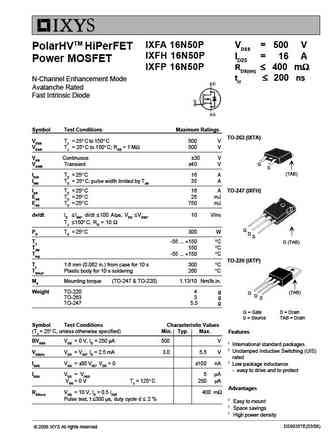
IXFA 16N50P VDSS = 500 V PolarHVTM HiPerFET IXFH 16N50P ID25 = 16 A Power MOSFET IXFP 16N50P RDS(on) 400 m trr 200 ns N-Channel Enhancement Mode Avalanche Rated Fast Intrinsic Diode Symbol Test Conditions Maximum Ratings TO-263 (IXTA) VDSS TJ = 25 C to 150 C 500 V VDGR TJ = 25 C to 150 C; RGS = 1 M 500 V
ixtc26n50p.pdf
IXTC 26N50P VDSS = 500 V PolarHVTM ID25 = 15 A Power MOSFET RDS(on) 260 m ISOPLUS220TM (Electrically Isolated Tab) N-Channel Enhancement Mode Avalanche Rated Symbol Test Conditions Maximum Ratings VDSS TJ = 25 C to 150 C 500 V ISOPLUS220TM (IXTC) E153432 VDGR TJ = 25 C to 150 C; RGS = 1 M 500 V VGS Continuous 30 V VGSM Transi
ixth36n50p ixtq36n50p ixtt36n50p ixtv36n50p.pdf

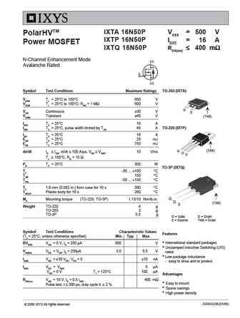
IXTH 36N50P VDSS = 500 V PolarHVTM IXTQ 36N50P ID25 = 36 A Power MOSFET IXTT 36N50P RDS(on) 170 m IXTV 36N50P N-Channel Enhancement Mode Avalanche Rated IXTV 36N50PS TO-3P (IXTQ) Symbol Test Conditions Maximum Ratings VDSS TJ = 25 C to 150 C 500 V G VDGR TJ = 25 C to 150 C; RGS = 1 M 500 V (TAB) D S VGS Continuous 30 V VGS
ixta6n50p ixtp6n50p.pdf
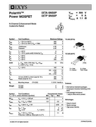
VDSS = 500 V IXTA 6N50P PolarHVTM ID25 = 6 A IXTP 6N50P Power MOSFET RDS(on) 1.1 N-Channel Enhancement Mode Avalanche Rated Symbol Test Conditions Maximum Ratings TO-263 (IXTA) VDSS TJ = 25 C to 150 C 500 V VDGR TJ = 25 C to 150 C; RGS = 1 M 500 V VGSS Continuous 30 V G S VGSM Transient 40 V (TAB) ID25 TC = 25 C6 A
ixfc26n50p.pdf
IXFC 26N50P VDSS = 500 V PolarHVTM HiPerFET ID25 = 15 A Power MOSFET RDS(on) 260 m ISOPLUS 220TM (Electrically Isolated Tab) trr 250 ns N-Channel Enhancement Mode Avalanche Rated Fast Intrinsic Diode Symbol Test Conditions Maximum Ratings ISOPLUS220TM (IXFC) E153432 VDSS TJ = 25 C to 150 C 500 V VDGR TJ = 25
ixth36n50p ixtq36n50p ixtt36n50p ixtv36n50p ixtv36n50ps.pdf
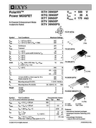
IXTH 36N50P VDSS = 500 V PolarHVTM IXTQ 36N50P ID25 = 36 A Power MOSFET IXTT 36N50P RDS(on) 170 m IXTV 36N50P N-Channel Enhancement Mode Avalanche Rated IXTV 36N50PS TO-3P (IXTQ) Symbol Test Conditions Maximum Ratings VDSS TJ = 25 C to 150 C 500 V G VDGR TJ = 25 C to 150 C; RGS = 1 M 500 V (TAB) D S VGS Continuous 30 V VGS
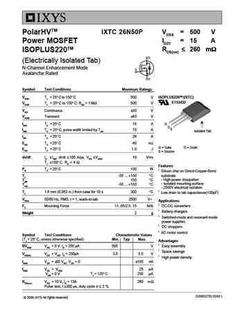
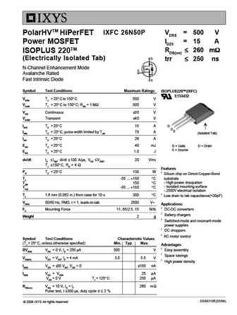
ixfj26n50p3.pdf
Advance Technical Information Polar3TM HiperFETTM VDSS = 500V IXFJ26N50P3 ID25 = 14A Power MOSFET RDS(on) 265m (Electrically Isolated Tab) N-Channel Enhancement Mode ISO TO-247TM Avalanche Rated E153432 Fast Intrinsic Rectifier Symbol Test Conditions Maximum Ratings G D Isolated Tab S VDSS TJ = 25 C to 150 C 500 V VDGR TJ = 25 C
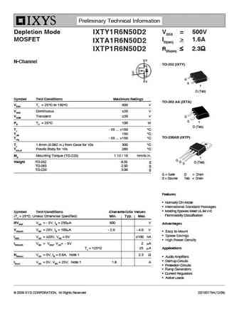
ixtp1r6n50p ixty1r6n50p.pdf
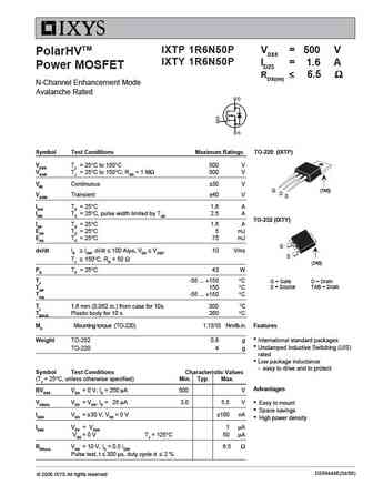
IXTP 1R6N50P VDSS = 500 V PolarHVTM IXTY 1R6N50P ID25 = 1.6 A Power MOSFET RDS(on) 6.5 N-Channel Enhancement Mode Avalanche Rated Symbol Test Conditions Maximum Ratings TO-220 (IXTP) VDSS TJ = 25 C to 150 C 500 V VDGR TJ = 25 C to 150 C; RGS = 1 M 500 V VGS Continuous 30 V G (TAB) D VGSM Transient 40 V S ID25 TC = 25 C 1.6 A IDM
ixfr24n50 ixfr26n50.pdf
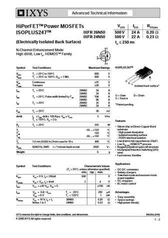
Advanced Technical Information VDSS ID25 RDS(on) HiPerFETTM Power MOSFETs IXFR 26N50 500 V 24 A 0.20 W ISOPLUS247TM IXFR 24N50 500 V 22 A 0.23 W (Electrically Isolated Back Surface) trr 250 ns N-Channel Enhancement Mode High dV/dt, Low trr, HDMOSTM Family ISOPLUS 247TM Symbol Test Conditions Maximum Ratings VDSS TJ = 25 C to 150 C 500 V VDGR TJ = 25 C to 150 C; RGS = 1 MW 50
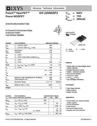
ixfa26n50p3 ixfh26n50p3 ixfp26n50p3 ixfq26n50p3.pdf
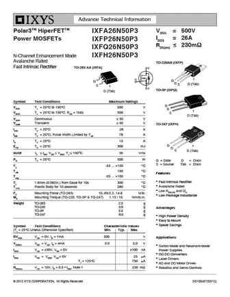
Advance Technical Information Polar3TM HiperFETTM VDSS = 500V IXFA26N50P3 ID25 = 26A Power MOSFETs IXFP26N50P3 RDS(on) 230m IXFQ26N50P3 N-Channel Enhancement Mode IXFH26N50P3 Avalanche Rated TO-220AB (IXFP) Fast Intrinsic Rectifier TO-263 AA (IXFA) G G D D (Tab) S S TO-3P (IXFQ) D (Tab) Symbol Test Conditions Maximum Ratings G VDSS TJ
ixfc16n50p.pdf
IXFC 16N50P VDSS = 500 V PolarHVTM HiPerFET ID25 = 10 A Power MOSFET RDS(on) 450 m ISOPLUS220TM trr 200 ns (Electrically Isolated Back Surface) N-Channel Enhancement Mode Fast Intrinsic Diode Avalanche Rated ISOPLUS220TM (IXFC) Symbol Test Conditions Maximum Ratings E153432 VDSS TJ = 25 C to 150 C 500 V VDGR T
ixty1r6n50d2 ixta1r6n50d2 ixtp1r6n50d2.pdf
Preliminary Technical Information Depletion Mode VDSX = 500V IXTY1R6N50D2 MOSFET ID(on) > 1.6A IXTA1R6N50D2 RDS(on) 2.3 IXTP1R6N50D2 N-Channel TO-252 (IXTY) G S D (Tab) Symbol Test Conditions Maximum Ratings TO-263 AA (IXTA) VDSX TJ = 25 C to 150 C 500 V VGSX Continuous 20 V VGSM Transient 30 V G S PD TC = 25 C 100 W D (Tab) TJ -
ixfa16n50p3 ixfh16n50p3 ixfp16n50p3.pdf
Advance Technical Information Polar3 TM HiPerFETTM VDSS = 500V IXFA16N50P3 Power MOSFETs ID25 = 16A IXFP16N50P3 RDS(on) 360m IXFH16N50P3 N-Channel Enhancement Mode TO-263 AA (IXFA) Avalanche Rated Fast Intrinsic Rectifier G S D (Tab) Symbol Test Conditions Maximum Ratings TO-220AB (IXFP) VDSS TJ = 25 C to 150 C 500 V VDGR TJ = 25 C to 15
ixtk46n50l ixtx46n50l.pdf
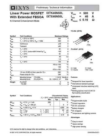
Preliminary Technical Information IXTK46N50L VDSS = 500 V Linear Power MOSFET IXTX46N50L ID25 = 46 A With Extended FBSOA RDS(on) 0.16 N-Channel Enhancement Mode TO-264 (IXTK) Symbol Test Conditions Maximum Ratings VDSS TJ = 25 C to 150 C 500 V VDGR TJ = 25 C to 150 C; RGS = 1 M 500 V G D VGS Continuous 30 V S (TAB) VGSM Transient
ixfr24n50q ixfr26n50q.pdf
VDSS ID25 RDS(on) HiPerFETTM Power MOSFETs IXFR 26N50Q 500 V 24 A 0.20 ISOPLUS247TM IXFR 24N50Q 500 V 22 A 0.23 (Electrically Isolated Back Surface) trr 250 ns N-Channel Enhancement Mode High dV/dt, Low t , HDMOSTM Family rr Symbol Test Conditions Maximum Ratings ISOPLUS 247TM E153432 VDSS TJ = 25 C to 150 C
ixta16n50p ixtp16n50p ixtq16n50p.pdf
IXTA 16N50P VDSS = 500 V PolarHVTM IXTP 16N50P ID25 = 16 A Power MOSFET IXTQ 16N50P RDS(on) 400 m N-Channel Enhancement Mode Avalanche Rated Symbol Test Conditions Maximum Ratings TO-263 (IXTA) VDSS TJ = 25 C to 150 C 500 V VDGR TJ = 25 C to 150 C; RGS = 1 M 500 V G VGS Continuous 30 V S VGSM Transient 40 V (TAB) ID25 TC = 25 C16 A
ixtq26n50p ixtt26n50p ixtv26n50p.pdf
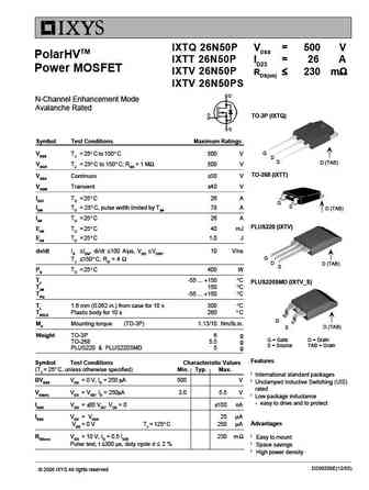
IXTQ 26N50P VDSS = 500 V PolarHVTM IXTT 26N50P ID25 = 26 A Power MOSFET IXTV 26N50P RDS(on) 230 m IXTV 26N50PS N-Channel Enhancement Mode Avalanche Rated TO-3P (IXTQ) Symbol Test Conditions Maximum Ratings G VDSS TJ = 25 C to 150 C 500 V D S D (TAB) VDGR TJ = 25 C to 150 C; RGS = 1 M 500 V TO-268 (IXTT) VGSS Continuos 30 V
ixfh36n50p ixft36n50p ixfv36n50p.pdf
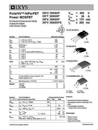
IXFH 36N50P VDSS = 500 V PolarHVTM HiPerFET IXFT 36N50P ID25 = 36 A Power MOSFET IXFV 36N50P RDS(on) 170 m N-Channel Enhancement Mode IXFV 36N50PS trr 200 ms Avalanche Rated Fast Intrinsic Diode TO-247 AD (IXFH) Symbol Test Conditions Maximum Ratings VDSS TJ = 25 C to 175 C 500 V VDGR TJ = 25 C to 175 C; RGS
ixfv26n50p ixfh26n50p.pdf
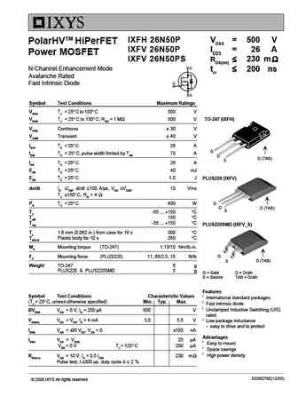
IXFH 26N50P VDSS = 500 V PolarHVTM HiPerFET IXFV 26N50P ID25 = 26 A Power MOSFET IXFV 26N50PS RDS(on) 230 m N-Channel Enhancement Mode trr 200 ns Avalanche Rated Fast Intrinsic Diode Symbol Test Conditions Maximum Ratings VDSS TJ = 25 C to 150 C 500 V VDGR TJ = 25 C to 150 C; RGS = 1 M 500 V TO-247 (IXFH)
ixtn46n50l.pdf
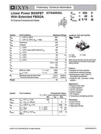
Preliminary Technical Information IXTN46N50L VDSS = 500 V Linear Power MOSFET ID25 = 46 A With Extended FBSOA D RDS(on) 0.16 N-Channel Enhancement Mode G S S Symbol Test Conditions Maximum Ratings miniBLOC, SOT-227 B (IXTN) E153432 VDSS TJ = 25 C to 150 C 500 V VDGR TJ = 25 C to 150 C; RGS = 1 M 500 V S G VGS Continuous 30 V VGSM
fqd6n50c.pdf

Is Now Part of To learn more about ON Semiconductor, please visit our website at www.onsemi.com Please note As part of the Fairchild Semiconductor integration, some of the Fairchild orderable part numbers will need to change in order to meet ON Semiconductor s system requirements. Since the ON Semiconductor product management systems do not have the ability to manage part nomenclatur
fdd6n50tm-f085.pdf
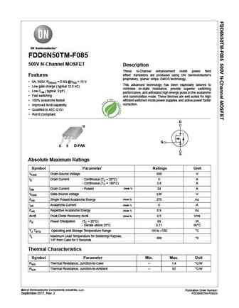
FDD6N50TM-F085 500V N-Channel MOSFET Description These N-Channel enhancement mode power field effect transistors are produced using ON Semiconductor's Features proprietary, planar stripe, DMOS technology. 6A, 500V, RDS(on) = 0.9 @VGS = 10 V This advanced technology has been especially tailored to Low gate charge ( typical 12.8 nC) minimize on-state resistance, provide s
fdd6n50 fdu6n50.pdf
FDD6N50 / FDU6N50 N-Channel UniFETTM MOSFET 500 V, 6 A, 900 m Description Features RDS(on) = 900 m (Max.) @ VGS = 10 V, ID = 3 A UniFETTM MOSFET is ON Semiconductor s high voltage MOSFET family based on planar stripe and DMOS technology. Low Gate Charge (Typ. 12.8 nC) This MOSFET is tailored to reduce on-state resistance, and to Low Crss (Typ. 9 pF) provide bet
fqaf16n50.pdf

Is Now Part of To learn more about ON Semiconductor, please visit our website at www.onsemi.com Please note As part of the Fairchild Semiconductor integration, some of the Fairchild orderable part numbers will need to change in order to meet ON Semiconductor s system requirements. Since the ON Semiconductor product management systems do not have the ability to manage part nomenclatur
fdd6n50f.pdf

Is Now Part of To learn more about ON Semiconductor, please visit our website at www.onsemi.com Please note As part of the Fairchild Semiconductor integration, some of the Fairchild orderable part numbers will need to change in order to meet ON Semiconductor s system requirements. Since the ON Semiconductor product management systems do not have the ability to manage part nomenclatur
fdpf16n50ut.pdf

Is Now Part of To learn more about ON Semiconductor, please visit our website at www.onsemi.com Please note As part of the Fairchild Semiconductor integration, some of the Fairchild orderable part numbers will need to change in order to meet ON Semiconductor s system requirements. Since the ON Semiconductor product management systems do not have the ability to manage part nomenclatur
26n50.pdf

UNISONIC TECHNOLOGIES CO., LTD 26N50 Preliminary Power MOSFET 26A, 500V N-CHANNEL POWER MOSFET DESCRIPTION The UTC 26N50 is an N-channel mode power MOSFET using UTC s advanced technology to provide customers with planar stripe and DMOS technology. This technology allows a minimum on-state resistance and superior switching performance. It also can withstand high energy pulse
16n50.pdf
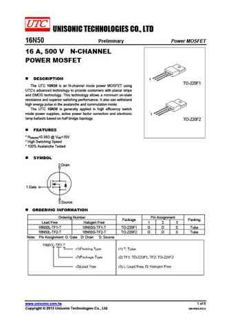
UNISONIC TECHNOLOGIES CO., LTD 16N50 Preliminary Power MOSFET 16 A, 500 V N-CHANNEL POWER MOSFET DESCRIPTION 1 TO-220F1 The UTC 16N50 is an N-channel mode power MOSFET using UTC s advanced technology to provide customers with planar stripe and DMOS technology. This technology allows a minimum on-state resistance and superior switching performance. It also can withstand
fmh16n50e.pdf
FMH16N50E FUJI POWER MOSFET Super FAP-E3 series N-CHANNEL SILICON POWER MOSFET Features Outline Drawings [mm] Equivalent circuit schematic Maintains both low power loss and low noise TO-3P(Q) Lower R (on) characteristic DS More controllable switching dv/dt by gate resistance Drain(D) Smaller V ringing waveform during switching GS Narrow band of the gate threshold voltage (3.0 0.5V)
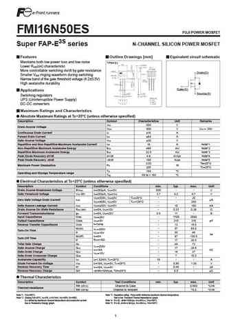
fmv16n50es.pdf
FMV16N50ES FUJI POWER MOSFET Super FAP-E3S series N-CHANNEL SILICON POWER MOSFET Features Outline Drawings [mm] Equivalent circuit schematic Maintains both low power loss and low noise TO-220F(SLS) Lower R (on) characteristic DS More controllable switching dv/dt by gate resistance Drain(D) Smaller V ringing waveform during switching GS Narrow band of the gate threshold voltage (4.2
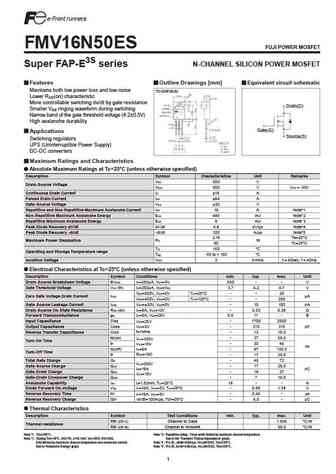
fmh16n50es.pdf
FMH16N50ES FUJI POWER MOSFET Super FAP-E3S series N-CHANNEL SILICON POWER MOSFET Features Outline Drawings [mm] Equivalent circuit schematic Maintains both low power loss and low noise TO-3P (Q) Lower R (on) characteristic DS More controllable switching dv/dt by gate resistance Drain(D) Smaller V ringing waveform during switching GS Narrow band of the gate threshold voltage (4.2 0.5
fmp16n50e.pdf
FMP16N50E FUJI POWER MOSFET Super FAP-E3 series N-CHANNEL SILICON POWER MOSFET Features Outline Drawings [mm] Equivalent circuit schematic Maintains both low power loss and low noise TO-220AB Lower R (on) characteristic DS More controllable switching dv/dt by gate resistance Drain(D) Smaller V ringing waveform during switching GS Narrow band of the gate threshold voltage (3.0 0.5V)
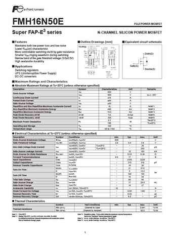
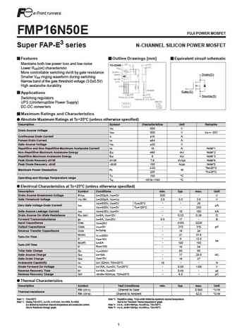
fmv16n50e.pdf
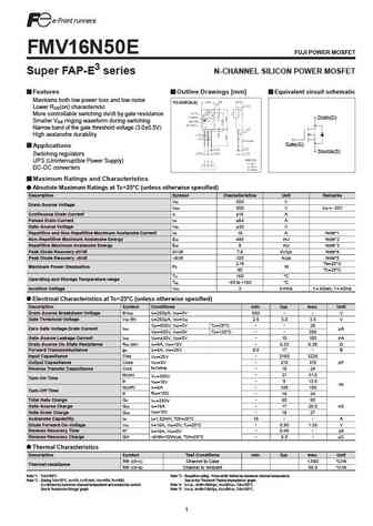
FMV16N50E FUJI POWER MOSFET Super FAP-E3 series N-CHANNEL SILICON POWER MOSFET Features Outline Drawings [mm] Equivalent circuit schematic Maintains both low power loss and low noise TO-220F(SLS) Lower R (on) characteristic DS More controllable switching dv/dt by gate resistance Drain(D) Smaller V ringing waveform during switching GS Narrow band of the gate threshold voltage (3.0 0.
fmb16n50e.pdf
SPECIFICATION Device Name Power MOSFET FMI16N50E (T-pack L) FMC16N50E (T-pack S) Type Name FMB16N50E (T-pack SJ) Spec. No. MS5F6867 Date July.-19-2007 Fuji Electric Device Technology Co.,Ltd. NAME DATE APPROVED Fuji Electric Device Technology Co., Ltd. DRAWN July.-19-'07 CHECKED July.-19-'07 MS5F6867 1 / 18 CHECKED July.-19-'07 H04-004-05 This m aterial and the inform a
fmi16n50es.pdf
FMI16N50ES FUJI POWER MOSFET Super FAP-E3S series N-CHANNEL SILICON POWER MOSFET Features Outline Drawings [mm] Equivalent circuit schematic Maintains both low power loss and low noise T-Pack (L) Lower R (on) characteristic DS More controllable switching dv/dt by gate resistance Drain(D) Smaller V ringing waveform during switching GS Narrow band of the gate threshold voltage (4.2 0.
fmc16n50es.pdf

FMC16N50ES FUJI POWER MOSFET Super FAP-E3S series N-CHANNEL SILICON POWER MOSFET Features Outline Drawings [mm] Equivalent circuit schematic Maintains both low power loss and low noise T-Pack (S) Lower R (on) characteristic DS More controllable switching dv/dt by gate resistance Drain(D) Smaller V ringing waveform during switching GS Narrow band of the gate threshold voltage (4.2 0.
fmc16n50e.pdf
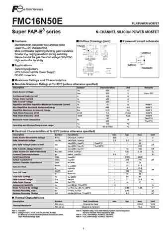
FMC16N50E FUJI POWER MOSFET Super FAP-E3 series N-CHANNEL SILICON POWER MOSFET Features Outline Drawings [mm] Equivalent circuit schematic Maintains both low power loss and low noise T-Pack(S) Lower R (on) characteristic DS More controllable switching dv/dt by gate resistance Drain(D) Smaller V ringing waveform during switching GS Narrow band of the gate threshold voltage (3.0 0.5V)
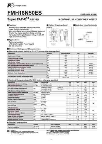
fmp16n50es.pdf
FMP16N50ES FUJI POWER MOSFET Super FAP-E3S series N-CHANNEL SILICON POWER MOSFET Features Outline Drawings [mm] Equivalent circuit schematic Maintains both low power loss and low noise TO-220AB Lower R (on) characteristic DS More controllable switching dv/dt by gate resistance Drain(D) Smaller V ringing waveform during switching GS Narrow band of the gate threshold voltage (4.2 0.5V
fml16n50es.pdf
http //www.fujisemi.com FML16N50ES FUJI POWER MOSFET Super FAP-E3 series N-CHANNEL SILICON POWER MOSFET Features Outline Drawings [mm] Equivalent circuit schematic Maintains both low power loss and low noise TFP 9.0 0.2 7.0 0.2 0.4 0.1 Lower R (on) characteristic DS 4 More controllable switching dv/dt by gate resistance 4 D Smaller V ringing waveform during switching GS Narrow
fmi16n50e.pdf

FMI16N50E FUJI POWER MOSFET Super FAP-E3 series N-CHANNEL SILICON POWER MOSFET Features Outline Drawings [mm] Equivalent circuit schematic Maintains both low power loss and low noise T-Pack(L) Lower R (on) characteristic DS More controllable switching dv/dt by gate resistance Drain(D) Smaller V ringing waveform during switching GS Narrow band of the gate threshold voltage (3.0 0.5V)
tsm6n50ch tsm6n50ci tsm6n50cp.pdf
TSM6N50 500V N-Channel Power MOSFET ITO-220 TO-252 TO-251 Pin Definition PRODUCT SUMMARY (DPAK) (IPAK) 1. Gate VDS (V) RDS(on)( ) ID (A) 2. Drain 3. Source 500 1.4 @ VGS =10V 2.8 General Description The TSM6N50 N-Channel enhancement mode Power MOSFET is produced by planar stripe DMOS technology. This advanced technology has been especially tailored to minimize on-s
kf16n50f.pdf
KF16N50P/F SEMICONDUCTOR N CHANNEL MOS FIELD TECHNICAL DATA EFFECT TRANSISTOR General Description KF16N50P A This planar stripe MOSFET has better characteristics, such as fast O C switching time, low on resistance, low gate charge and excellent F avalanche characteristics. It is mainly suitable for active power factor E DIM MILLIMETERS G correction and switching mode power supp
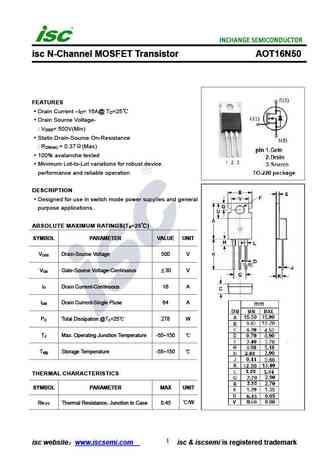
aot16n50 aotf16n50.pdf
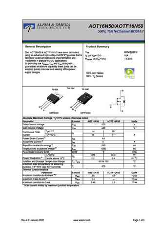
AOT16N50/AOTF16N50 500V, 16A N-Channel MOSFET General Description Product Summary VDS 600V@150 The AOT16N50 & AOTF16N50 have been fabricated using an advanced high voltage MOSFET process that is ID (at VGS=10V) 16A designed to deliver high levels of performance and RDS(ON) (at VGS=10V)
aod6n50.pdf
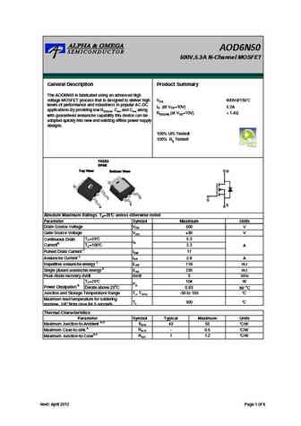
AOD6N50 500V,5.3A N-Channel MOSFET General Description Product Summary The AOD6N50 is fabricated using an advanced high voltage MOSFET process that is designed to deliver high VDS 600V@150 levels of performance and robustness in popular AC-DC ID (at VGS=10V) 5.3A applications.By providing low RDS(on), Ciss and Crss along RDS(ON) (at VGS=10V)
aot16n50.pdf
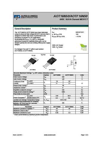
AOT16N50/AOTF16N50 500V, 16A N-Channel MOSFET General Description Product Summary VDS 600V@150 The AOT16N50 & AOTF16N50 have been fabricated using an advanced high voltage MOSFET process that is ID (at VGS=10V) 16A designed to deliver high levels of performance and RDS(ON) (at VGS=10V)
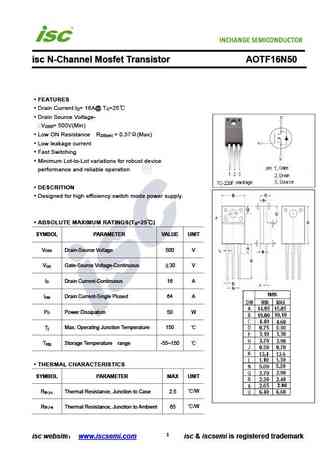
aotf16n50.pdf

AOT16N50/AOTF16N50 500V, 16A N-Channel MOSFET General Description Product Summary VDS 600V@150 The AOT16N50 & AOTF16N50 have been fabricated using an advanced high voltage MOSFET process that is ID (at VGS=10V) 16A designed to deliver high levels of performance and RDS(ON) (at VGS=10V)
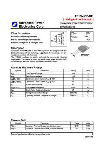
ap16n50p.pdf

AP16N50P-HF Halogen-Free Product Advanced Power N-CHANNEL ENHANCEMENT MODE Electronics Corp. POWER MOSFET Low On-resistance D BVDSS 500V Simple Drive Requirement RDS(ON) 0.4 Fast Switching Characteristic ID 16A G RoHS Compliant & Halogen-Free S Description AP16N50 series are from Advanced Power innovated
ap16n50i-hf.pdf

AP16N50I-HF Halogen-Free Product Advanced Power N-CHANNEL ENHANCEMENT MODE Electronics Corp. POWER MOSFET D Low On-resistance BVDSS 500V Simple Drive Requirement RDS(ON) 0.4 Fast Switching Characteristic ID 16A G RoHS Compliant & Halogen-Free S Description Advanced Power MOSFETs from APEC provide the designer with the best combination of fast switching, ruggedized
ap16n50w-hf.pdf

AP16N50W-HF Halogen-Free Product Advanced Power N-CHANNEL ENHANCEMENT MODE Electronics Corp. POWER MOSFET D Low On-resistance BVDSS 500V Simple Drive Requirement RDS(ON) 0.4 Fast Switching Characteristic ID 16A G RoHS Compliant & Halogen-Free S Description Advanced Power MOSFETs from APEC provide the designer with the best combination of fast switching, ruggedized
ap16n50p-hf.pdf
AP16N50P-HF Halogen-Free Product Advanced Power N-CHANNEL ENHANCEMENT MODE Electronics Corp. POWER MOSFET Low On-resistance D BVDSS 500V Simple Drive Requirement RDS(ON) 0.4 Fast Switching Characteristic ID 16A G RoHS Compliant & Halogen-Free S Description Advanced Power MOSFETs from APEC provide the designer with the best combination of fast switching, ruggedized
ap16n50i.pdf
AP16N50I-HF Halogen-Free Product Advanced Power N-CHANNEL ENHANCEMENT MODE Electronics Corp. POWER MOSFET D Low On-resistance BVDSS 500V Simple Drive Requirement RDS(ON) 0.4 Fast Switching Characteristic ID3 16A G RoHS Compliant & Halogen-Free S Description AP16N50 series are from Advanced Power innovated design and silicon process technology to achieve the lowest
ap16n50w.pdf

AP16N50W RoHS-compliant Product Advanced Power N-CHANNEL ENHANCEMENT MODE Electronics Corp. POWER MOSFET D Low On-resistance BVDSS 500V Simple Drive Requirement RDS(ON) 0.4 Fast Switching Characteristic ID 16A G S Description Advanced Power MOSFETs from APEC provide the designer with the best combination of fast switching, ruggedized device design, low on-resistance a
16n50.pdf
GOFORD 16N50 500V N-Channel MOSFET GENERAL DESCRIPTION VDSS RDS(ON) ID This Power MOSFET is produced using advanced planar stripe DMOS technology. 500V 0.38 16A This advanced technology has been especially tailored to minimize on-state resistance, provide superior switching performance, and withstand high energy pulse in the avalanche and commutation mode. These devices are well
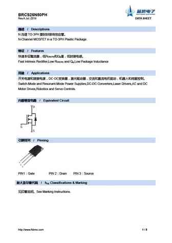
brcs26n50pa.pdf
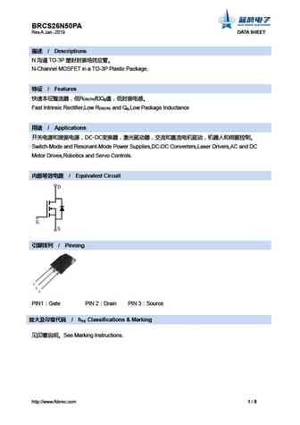
BRCS26N50PA Rev.A Jan.-2019 DATA SHEET / Descriptions N TO-3P N-Channel MOSFET in a TO-3P Plastic Package. / Features RDS(ON) Qg Fast Intrinsic Rectifier,Low RDS(ON) and Qg,Low Package Inductance / Applications DC-DC
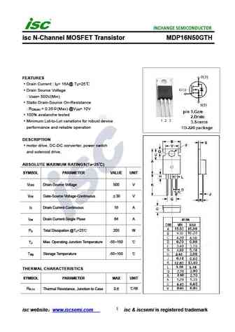
mdf16n50gth mdp16n50gth.pdf
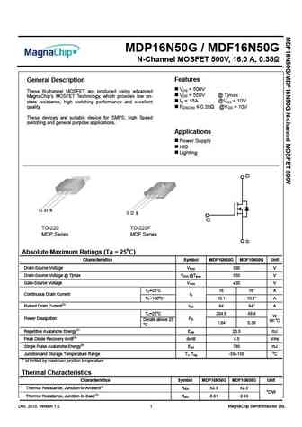
MDP16N50G / MDF16N50G N-Channel MOSFET 500V, 16.0 A, 0.35 General Description Features VDS = 500V These N-channel MOSFET are produced using advanced VDS = 550V @ Tjmax MagnaChip s MOSFET Technology, which provides low on- ID = 16A @VGS = 10V state resistance, high switching performance and excellent RDS(ON) 0.35 @VGS = 10V quality. These devices are suitable d
mdq16n50gth mdq16n50gtp.pdf
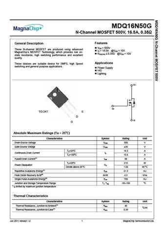
MDQ16N50G N-Channel MOSFET 500V, 16.5A, 0.35 General Description Features V = 500V DS These N-channel MOSFET are produced using advanced I = 16.5A @V = 10V D GS MagnaChip s MOSFET Technology, which provides low on- R 0.35 @V = 10V DS(ON) GS state resistance, high switching performance and excellent quality. Applications These devices are suitab
msw16n50.pdf
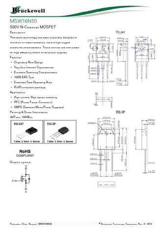
MSW16N50 500V N-Channel MOSFET Description TO-247 This latest technology has been especially designed to minimize on-state resistance, have a high rugged avalanche characteristics. These devices are well suited for high efficiency switch mode power supplies. Features Originative New Design Very Low Intrinsic Capacitances Excellent Switching Characteristics
msf16n50.pdf
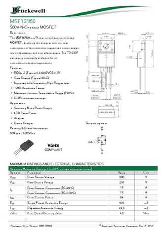
MSF16N50 500V N-Channel MOSFET Description The MSF16N50 is a N-channel enhancement-mode MOSFET , providing the designer with the best combination of fast switching, ruggedized device design, low on-resistance and cost effectiveness. The TO-220F package is universally preferred for all commercial-industrial applications Features RDS(on) (Typical 0.33 )@VGS=10V Gate
jfpc16n50c jffm16n50c.pdf
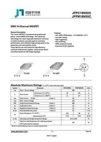
JFPC16N50C JFFM16N50C 500V N-Channel MOSFET General Description Features This Power MOSFET is produced using advanced - 16A, 500V, RDS(on)typ. = 0.33 @VGS = 10 V planar stripe DMOS technology. This advanced - Low gate charge technology has been especially tailored to minimize - High ruggedness on-state resistance, provide superior switching - Fast switching performanc
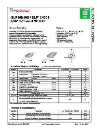
slp16n50c slf16n50c.pdf
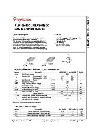
SLP16N50C / SLF16N50C 500V N-Channel MOSFET General Description Features This Power MOSFET is produced using Maple semi s - 16A, 500V, RDS(on)typ. = 305m @VGS = 10 V advanced planar stripe DMOS technology. - Low gate charge ( typical 52nC) This advanced technology has been especially tailored - High ruggedness to minimize on-state resistance, provide superior switching - Fast switching
slp16n50s slf16n50s.pdf
SLP16N50S / SLF16N50S 500V N-Channel MOSFET General Description Features This Power MOSFET is produced using Maple semi s - 16A, 500V, RDS(on) = 280m @VGS = 10 V advanced planar stripe DMOS technology. - Low gate charge ( typical 31nC) This advanced technology has been especially tailored - Low Crss ( typical 6.8pF) to minimize on-state resistance, provide superior switching - High rug
smos21n50 smos26n50.pdf
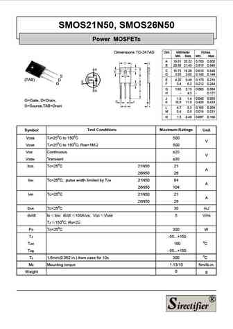
SMOS21N50, SMOS26N50 Power MOSFETs Dimensions TO-247AD Dim. Millimeter Inches Min. Max. Min. Max. A 19.81 20.32 0.780 0.800 B 20.80 21.46 0.819 0.845 C 15.75 16.26 0.610 0.640 D 3.55 3.65 0.140 0.144 S (TAB) E 4.32 5.49 0.170 0.216 D G F 5.4 6.2 0.212 0.244 G 1.65 2.13 0.065 0.084 H - 4.5 - 0.177 J 1.0 1.4 0.040 0.055 G=Gate, D=Drain, K 10.8 11.0 0.426 0.433 S=Source,TAB=Drain
tsf16n50mr.pdf
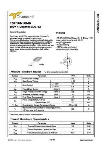
TSF16N50MR 500V N-Channel MOSFET General Description Features This Power MOSFET is produced using Truesemi s 16.0A,500V,Max.RDS(on)=0.4 @ VGS =10V advanced planar stripe DMOS technology. This advanced technology has been especially tailored to Low gate charge(typical 32nC) minimize on-state resistance, provide superior switching High ruggedness performance, and withs
fir16n50fg.pdf
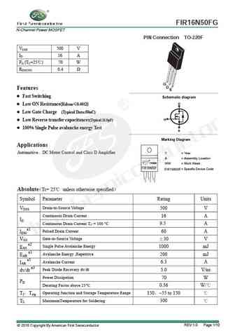
FIR16N50FG CREAT BY ART N-Channel Power MOSFET PIN Connection TO-220F VDSS 500 V ID 16 A PD (TC=25 ) 70 W RDS(ON) 0.4 G D S Features Fast Switching g Schematic dia ram D Low ON Resistance(Rdson 0.40 ) Low Gate Charge (Typical Data 50nC) G Low Reverse transfer capacitances(Typical 25.5pF) 100% Single Pulse avalanche energy Test S Marking Diagram Ap
hm16n50 hm16n50f.pdf
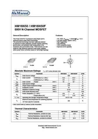
HM16N50 / HM16N50F 500V N-Channel MOSFET General Description Features This Power MOSFET is produced using Maple semi s - 16A, 500V, RDS(on)typ. = 305m @VGS = 10 V advanced planar stripe DMOS technology. - Low gate charge ( typical 52nC) This advanced technology has been especially tailored - High ruggedness to minimize on-state resistance, provide superior switching - Fast switching p
fdd6n50tm.pdf
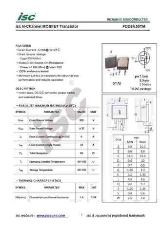
isc N-Channel MOSFET Transistor FDD6N50TM FEATURES Drain Current I =6A@ T =25 D C Drain Source Voltage V =500V(Min) DSS Static Drain-Source On-Resistance R =0.9 (Max) @ V = 10V DS(on) GS 100% avalanche tested Minimum Lot-to-Lot variations for robust device performance and reliable operation DESCRIPTION motor drive, DC-DC converter, power switch and solenoid
spp16n50c3.pdf
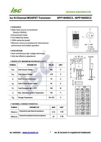
isc N-Channel MOSFET Transistor SPP16N50C3 ISPP16N50C3 FEATURES Static drain-source on-resistance RDS(on) 280m Enhancement mode Fast Switching Speed 100% avalanche tested Minimum Lot-to-Lot variations for robust device performance and reliable operation DESCRITION New revolutionary high voltage technology Ultra low effective capacitance ABSOLUTE MAXIMUM
ixtq26n50p.pdf
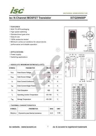
isc N-Channel MOSFET Transistor IXTQ26N50P FEATURES With TO-3PN packaging High speed switching Standard level gate drive Easy to use 100% avalanche tested Minimum Lot-to-Lot variations for robust device performance and reliable operation APPLICATIONS Power supply Switching applications ABSOLUTE MAXIMUM RATINGS(T =25 ) a SYMBOL PARAMETER VALUE UNIT V Drain-
ixtq36n50p.pdf
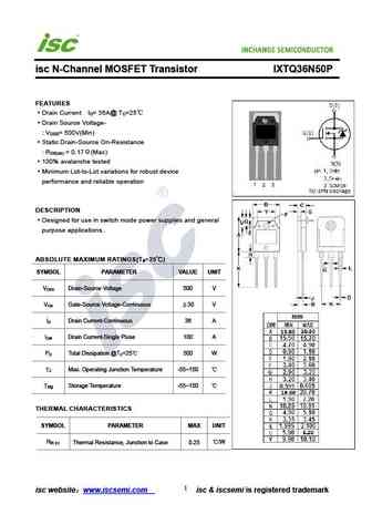
isc N-Channel MOSFET Transistor IXTQ36N50P FEATURES Drain Current I = 36A@ T =25 D C Drain Source Voltage- V = 500V(Min) DSS Static Drain-Source On-Resistance R = 0.17 (Max) DS(on) 100% avalanche tested Minimum Lot-to-Lot variations for robust device performance and reliable operation DESCRIPTION Designed for use in switch mode power supplies and general purpo
mdp16n50gth.pdf
isc N-Channel MOSFET Transistor MDP16N50GTH FEATURES Drain Current I = 16A@ T =25 D C Drain Source Voltage V = 500V(Min) DSS Static Drain-Source On-Resistance R = 0.35 (Max) @V = 10V DS(on) GS 100% avalanche tested Minimum Lot-to-Lot variations for robust device performance and reliable operation DESCRIPTION motor drive, DC-DC converter, power switch and sol
mdq16n50gtp.pdf
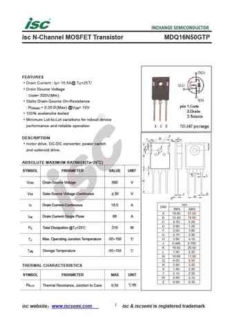
isc N-Channel MOSFET Transistor MDQ16N50GTP FEATURES Drain Current I = 16.5A@ T =25 D C Drain Source Voltage V = 500V(Min) DSS Static Drain-Source On-Resistance R = 0.35 (Max) @V = 10V DS(on) GS 100% avalanche tested Minimum Lot-to-Lot variations for robust device performance and reliable operation DESCRIPTION motor drive, DC-DC converter, power switch and s
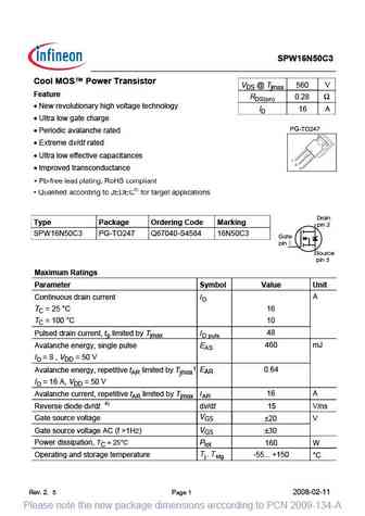
spw16n50c3.pdf
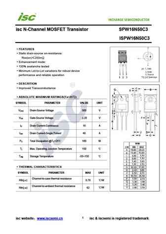
isc N-Channel MOSFET Transistor SPW16N50C3 ISPW16N50C3 FEATURES Static drain-source on-resistance RDS(on) 280m Enhancement mode 100% avalanche tested Minimum Lot-to-Lot variations for robust device performance and reliable operation DESCRITION Improved Transconductance ABSOLUTE MAXIMUM RATINGS(T =25 ) a SYMBOL PARAMETER VALUE UNIT V Drain-Source Voltage 50
aot16n50.pdf
isc N-Channel MOSFET Transistor AOT16N50 FEATURES Drain Current I = 16A@ T =25 D C Drain Source Voltage- V = 500V(Min) DSS Static Drain-Source On-Resistance R = 0.37 (Max) DS(on) 100% avalanche tested Minimum Lot-to-Lot variations for robust device performance and reliable operation DESCRIPTION Designed for use in switch mode power supplies and general purp
aotf16n50.pdf
isc N-Channel Mosfet Transistor AOTF16N50 FEATURES Drain Current I = 16A@ T =25 D C Drain Source Voltage- V = 500V(Min) DSS Low ON Resistance R = 0.37 (Max) DS(on) Low leakage current Fast Switching Minimum Lot-to-Lot variations for robust device performance and reliable operation DESCRITION Designed for high efficiency switch mode power supply. ABSOLUTE
fdd6n50f.pdf
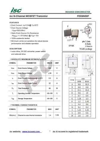
isc N-Channel MOSFET Transistor FDD6N50F FEATURES Drain Current I =5.5A@ T =25 D C Drain Source Voltage V =500V(Min) DSS Static Drain-Source On-Resistance R =1.15 (Max) @ V = 10V DS(on) GS 100% avalanche tested Minimum Lot-to-Lot variations for robust device performance and reliable operation DESCRIPTION motor drive, DC-DC converter, power switch and solenoi
Другие IGBT... 1N50, 1N50Z, 2N50, 3N50, 3N50Z, 4N50, 5N50, 5N50K, IRLB4132, 7N50, 8N50, 1N40, 2N40, 3N40, 4N40, 5N40, 6N40
Параметры MOSFET. Взаимосвязь и компромиссы
History: UF460
🌐 : EN ES РУ

Список транзисторов
Обновления
MOSFET: CEZC2P07 | CEZ2R05 | CEU3133 | CES2361 | CES2312A | CEP100N10L | CEM3425 | CEM3139 | CEM3133 | CEM3115 | CED3133 | CEC3257 | CEC2533 | CEB100N10L | BC3134KT | BC3134K
Popular searches
c2240 transistor | 2sc1918 | c1213 transistor | 2sc1400 replacement | 2sb817 | mn2488 datasheet | c2026 transistor | 2n3903 transistor