AO3418. Аналоги и основные параметры
Наименование производителя: AO3418
Тип транзистора: MOSFET
Полярность: N
Предельные значения
Pd ⓘ - Максимальная рассеиваемая мощность: 1.4 W
|Vds|ⓘ - Максимально допустимое напряжение сток-исток: 30 V
|Vgs|ⓘ - Максимально допустимое напряжение затвор-исток: 12 V
|Id| ⓘ - Максимально допустимый постоянный ток стока: 3.8 A
Tj ⓘ - Максимальная температура канала: 150 °C
Электрические характеристики
tr ⓘ - Время нарастания: 1.5 ns
Cossⓘ - Выходная емкость: 35 pf
RDSonⓘ - Сопротивление сток-исток открытого транзистора: 0.055 Ohm
Тип корпуса: SOT23
Аналог (замена) для AO3418
- подборⓘ MOSFET транзистора по параметрам
AO3418 даташит
ao3418.pdf
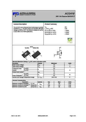
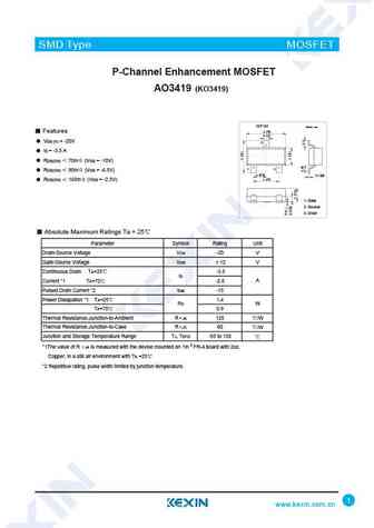
AO3418 30V N-Channel MOSFET General Description Product Summary VDS 30V The AO3418 uses advanced trench technology to provide excellent RDS(ON), low gate charge and operation with gate ID (at VGS=10V) 3.8A voltages as low as 2.5V. This device is suitable for use as RDS(ON) (at VGS=10V)
ao3418.pdf
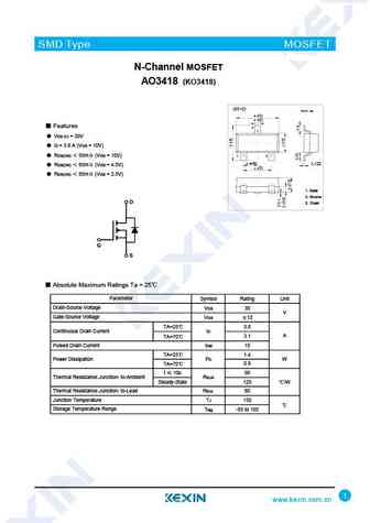
SMD Type MOSFET N-Channel MOSFET AO3418 (KO3418) SOT-23 Unit mm +0.1 2.9 -0.1 +0.1 0.4-0.1 Features 3 VDS (V) = 30V ID = 3.8 A (VGS = 10V) RDS(ON) 55m (VGS = 10V) 1 2 +0.1 +0.05 0.95 -0.1 0.1 -0.01 RDS(ON) 65m (VGS = 4.5V) +0.1 1.9 -0.1 RDS(ON) 85m (VGS = 2.5V) 1. Gate 2. Source D D 3. Drain G G S S Absolute Maxi
ao3418-3.pdf

SMD Type MOSFET N-Channel MOSFET AO3418 (KO3418) SOT-23-3 Unit mm +0.2 2.9-0.1 +0.1 0.4 -0.1 3 Features VDS (V) = 30V ID = 3.8 A (VGS = 10V) 1 2 RDS(ON) 55m (VGS = 10V) +0.02 +0.1 0.15 -0.02 0.95 -0.1 +0.1 1.9 -0.2 RDS(ON) 65m (VGS = 4.5V) RDS(ON) 85m (VGS = 2.5V) 1. Gate 2. Source 3. Drain D D G G S S Absolute
ao3419l.pdf
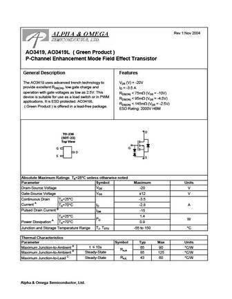
Rev 1 Nov 2004 AO3419, AO3419L ( Green Product ) P-Channel Enhancement Mode Field Effect Transistor General Description Features The AO3419 uses advanced trench technology to VDS (V) = -20V provide excellent RDS(ON), low gate charge and ID = -3.5 A operation with gate voltages as low as 2.5V. This RDS(ON)
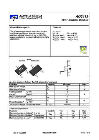
ao3413l.pdf
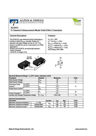
AO3413 P-Channel Enhancement Mode Field Effect Transistor General Description Features The AO3413/L uses advanced trench technology to VDS (V) = -20V provide excellent RDS(ON), low gate charge and ID = -3 A (VGS = -4.5V) operation with gate voltages as low as 1.8V. This RDS(ON)
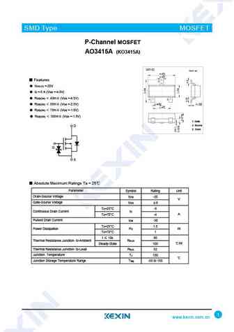
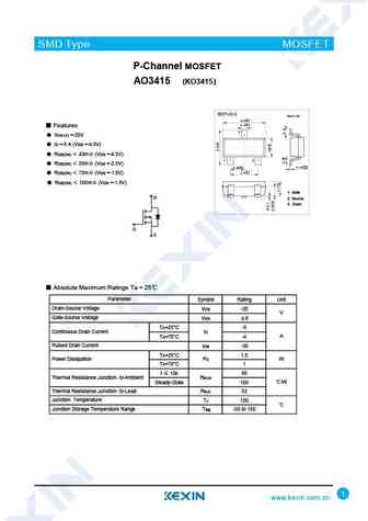
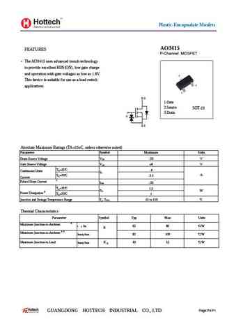
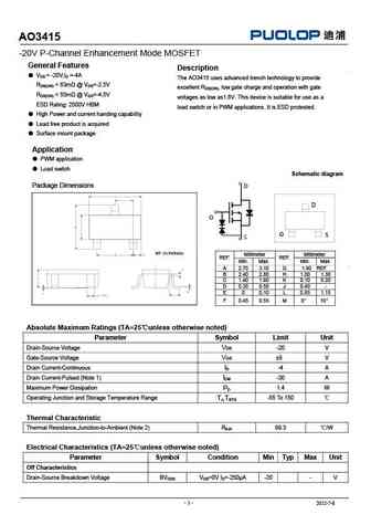
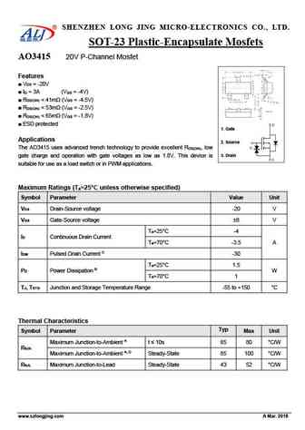
ao3415.pdf
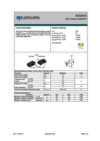
AO3415 20V P-Channel MOSFET General Description Product Summary VDS -20V The AO3415 uses advanced trench technology to provide excellent RDS(ON), low gate charge and operation with gate ID (at VGS=-4.5V) -4A voltages as low as 1.8V. This device is suitable for use as RDS(ON) (at VGS= -4.5V)
ao3415a.pdf
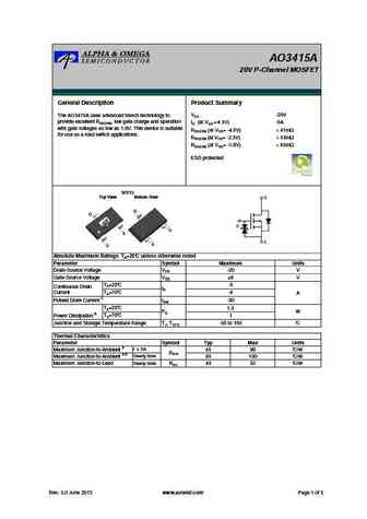
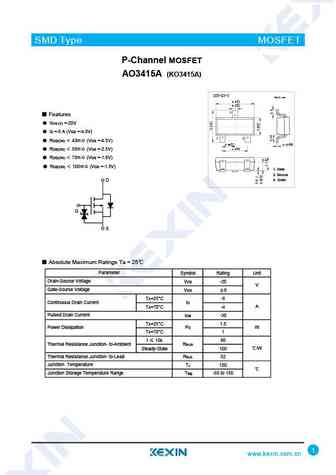
AO3415A 20V P-Channel MOSFET General Description Product Summary VDS -20V The AO3415A uses advanced trench technology to provide excellent RDS(ON), low gate charge and operation ID (at VGS=-4.5V) -5A with gate voltages as low as 1.8V. This device is suitable RDS(ON) (at VGS= -4.5V)
ao3413.pdf
AO3413 20V P-Channel MOSFET General Description Features General Description Features The AO3413 uses advanced trench technology to VDS = -20V The AO3413 uses advanced trench technology to VDS = -20V provide excellent RDS(ON), low gate charge and ID = -3A (VGS = -4.5V) provide excellent RDS(ON), low gate charge and ID = -3A (VGS = -4.5V) operation with gate voltages as low as 1.8V. This
ao3416.pdf
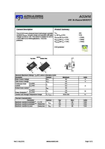
AO3416 20V N-Channel MOSFET General Description Product Summary VDS 20V The AO3416 uses advanced trench technology to provide excellent RDS(ON), low gate charge and operation with gate ID (at VGS=4.5V) 6.5A voltages as low as 1.8V. This device is suitable for use as RDS(ON) (at VGS=4.5V)
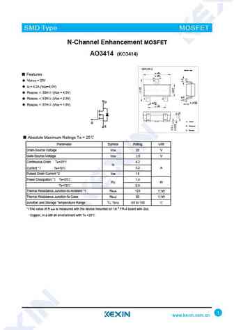
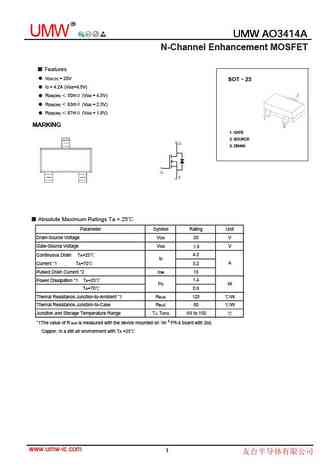
ao3414.pdf
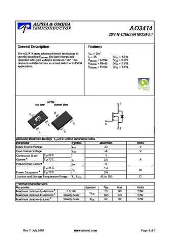
AO3414 20V N-Channel MOSFET General Description Features General Description Features The AO3414 uses advanced trench technology to VDS = 20V The AO3414 uses advanced trench technology to VDS = 20V provide excellent RDS(ON), low gate charge and ID = 3A (VGS = 4.5V) provide excellent RDS(ON), low gate charge and ID = 3A (VGS = 4.5V) operation with gate voltages as low as 1.8V. This ope
ao3419.pdf
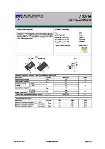
AO3419 20V P-Channel MOSFET General Description Product Summary VDS -20V The AO3419 uses advanced trench technology to provide excellent RDS(ON), low gate charge and operation with gate ID (at VGS=-10V) -3.5A voltages as low as 2.5V. This device is suitable for use as RDS(ON) (at VGS= -10V)
ao3415c.pdf
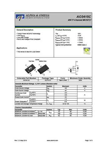
AO3415C 20V P-Channel MOSFET General Description Product Summary VDS Trench Power MOSFET technology -20V Low RDS(ON) ID (at VGS=-4.5V) -4.5A Low Gate Charge RDS(ON) (at VGS=-4.5V)
ao3415.pdf
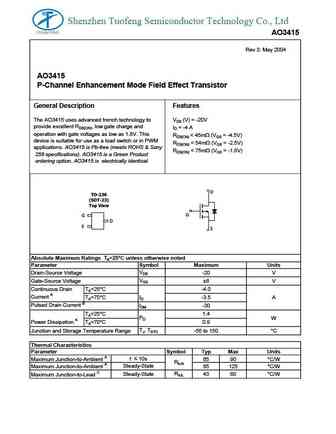
Shenzhen Tuofeng Semiconductor Technology Co., Ltd AO3415 Rev 3 May 2004 AO3415 P-Channel Enhancement Mode Field Effect Transistor General Description Features The AO3415 uses advanced trench technology to VDS (V) = -20V provide excellent RDS(ON), low gate charge and ID = -4 A operation with gate voltages as low as 1.8V. This RDS(ON)
ao3416.pdf
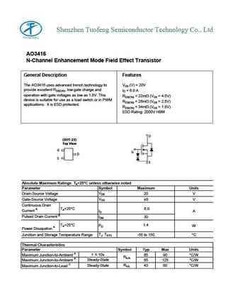
Shenzhen Tuofeng Semiconductor Technology Co., Ltd AO3416 N-Channel Enhancement Mode Field Effect Transistor General Description Features The AO3416 uses advanced trench technology to VDS (V) = 20V provide excellent RDS(ON), low gate charge and ID = 6.0 A operation with gate voltages as low as 1.8V. This RDS(ON)
ao3410.pdf
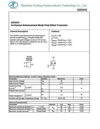
Shenzhen Tuofeng Semiconductor Technology Co., Ltd AO3410 AO3410 N-Channel Enhancement Mode Field Effect Transistor General Description Features The AO3410 uses advanced trench technology to VDS (V) = 30V provide excellent RDS(ON), low gate charge and ID = 5.0 A operation with gate voltages as low as 1.8V and as RDS(ON)
ao3414.pdf
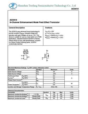
Shenzhen Tuofeng Semiconductor Technology Co., Ltd AO3414 AO3414 N-Channel Enhancement Mode Field Effect Transistor General Description Features The AO3414 uses advanced trench technology to VDS (V) = 20V provide excellent RDS(ON), low gate charge and ID = 4.2 A (VGS = 4.5V) operation with gate voltages as low as 1.8V. This RDS(ON)
ao3415.pdf
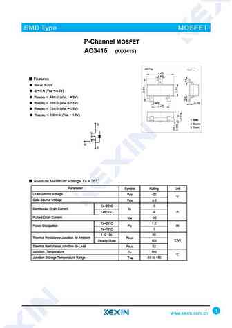
SMD Type MOSFET P-Channel MOSFET AO3415 (KO3415) SOT-23 Unit mm +0.1 2.9-0.1 +0.1 0.4 -0.1 Features 3 VDS (V) =-20V ID =-5 A (VGS =-4.5V) RDS(ON) 43m (VGS =-4.5V) 1 2 +0.1 0.95-0.1 0.1+0.05 RDS(ON) 55m (VGS =-2.5V) -0.01 +0.1 1.9-0.1 RDS(ON) 75m (VGS =-1.8V) RDS(ON) 100m (VGS =-1.5V) 1. Gate 2. Source D 3. Drain
ao3415a.pdf
SMD Type MOSFET P-Channel MOSFET AO3415A (KO3415A) SOT-23 Unit mm +0.1 2.9-0.1 +0.1 0.4 -0.1 Features 3 VDS (V) =-20V ID =-5 A (VGS =-4.5V) RDS(ON) 43m (VGS =-4.5V) 1 2 +0.1 0.95-0.1 0.1+0.05 RDS(ON) 55m (VGS =-2.5V) -0.01 +0.1 1.9-0.1 RDS(ON) 75m (VGS =-1.8V) RDS(ON) 100m (VGS =-1.5V) 1. Gate 2. Source D 3. Dra
ao3413-3.pdf

SMD Type MOSFET P-Channel MOSFET AO3413 (KO3413) SOT-23-3 Unit mm +0.2 2.9-0.1 +0.1 0.4 -0.1 3 Features VDS (V) =-20V ID =-3 A (VGS =-4.5V) 1 2 RDS(ON) 80m (VGS =-4.5V) +0.02 +0.1 0.15 -0.02 0.95 -0.1 RDS(ON) 100m (VGS =-2.5V) +0.1 1.9-0.2 RDS(ON) 130m (VGS =-1.8V) 1. Gate 2. Source D D 3. Drain G G S S Absolute
ao3415w.pdf
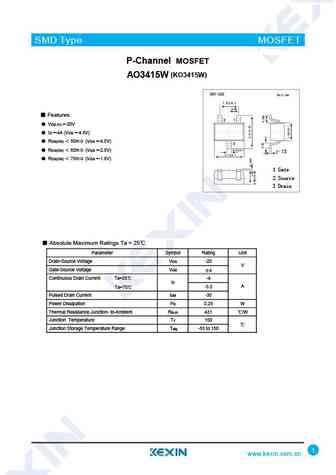
SMD Type MOSFET P-Channel MOSFET (KO3415W) AO3415W Features VDS (V) =-20V ID =-4A (VGS =-4.5V) RDS(ON) 50m (VGS =-4.5V) RDS(ON) 60m (VGS =-2.5V) RDS(ON) 75m (VGS =-1.8V) 1 Gate 2 Source 3 Drain Absolute Maximum Ratings Ta = 25 Parameter Symbol Rating Unit Drain-Source Voltage VDS -20 V Gate-Source Voltage VGS 8 Conti
ao3413.pdf
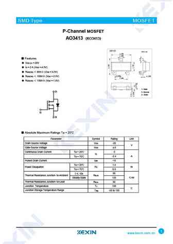
SMD Type MOSFET P-Channel MOSFET AO3413 (KO3413) SOT-23 Unit mm +0.1 2.9-0.1 +0.1 0.4 -0.1 Features 3 VDS (V) =-20V ID =-3 A (VGS =-4.5V) RDS(ON) 80m (VGS =-4.5V) 1 2 +0.1 0.95-0.1 0.1+0.05 -0.01 RDS(ON) 100m (VGS =-2.5V) +0.1 1.9-0.1 RDS(ON) 130m (VGS =-1.8V) 1. Gate D D 2. Source 3. Drain G G S S Absolute Maxim
ao3416.pdf
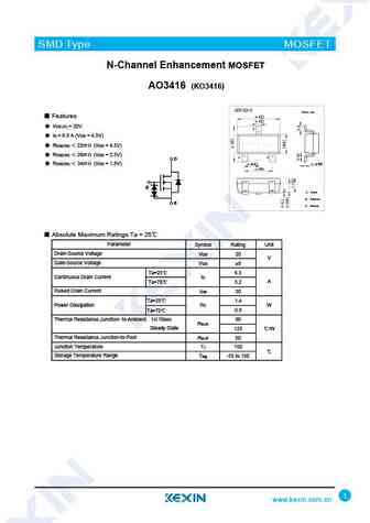
SMD Type MOSFET N-Channel Enhancement MOSFET AO3416 (KO3416) SOT-23-3 Unit mm +0.2 Features 2.9 -0.1 +0.1 0.4-0.1 VDS (V) = 20V 3 ID = 6.5 A (VGS = 4.5V) RDS(ON) 22m (VGS = 4.5V) RDS(ON) 26m (VGS = 2.5V) 1 2 D D +0.02 +0.1 RDS(ON) 34m (VGS = 1.8V) 0.15 -0.02 0.95 -0.1 +0.1 1.9 -0.2 G G 1. Gate 2. Source S S 3. Drain
ao3410.pdf
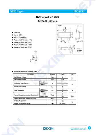
SMD Type MOSFET N-Channel MOSFET AO3410 (KO3410) SOT-23 Unit mm +0.1 2.9 -0.1 +0.1 0.4 -0.1 3 Features VDS (V) = 30V ID = 5.8 A (VGS = 10V) 1 2 RDS(ON) 28m (VGS = 10V) +0.1 +0.05 0.95-0.1 0.1 -0.01 +0.1 1.9 -0.1 RDS(ON) 33m (VGS = 4.5V) RDS(ON) 52m (VGS = 2.5V) RDS(ON) 70m (VGS = 1.8V) 1. Gate 2. Source 3. Drain
ao3416 ko3416.pdf
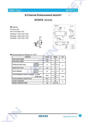
SMD Type MOSFET N-Channel Enhancement MOSFET AO3416 (KO3416) Features VDS (V) = 20V 3 ID = 6.5 A (VGS = 4.5V) RDS(ON) 22m (VGS = 4.5V) RDS(ON) 26m (VGS = 2.5V) 12 D D RDS(ON) 34m (VGS = 1.8V) G G S S Absolute Maximum Ratings Ta
ao3414.pdf
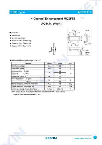
SMD Type IC SMD Type MOSFET N-Channel Enhancement MOSFET AO3414 (KO3414) SOT-23 Unit mm +0.1 2.9 -0.1 +0.1 Features 0.4 -0.1 3 VDS (V) = 20V ID = 4.2A (VGS=4.5V) RDS(ON) 50m (VGS = 4.5V) 1 2 +0.1 +0.05 RDS(ON) 63m (VGS = 2.5V) 0.95 -0.1 0.1 -0.01 +0.1 1.9 -0.1 RDS(ON) 87m (VGS = 1.8V) 1.Base 1. Gate 2.Emitter 2. Source 3. Drain 3.collector Absolute Maximum Ratings T
ao3419-3.pdf
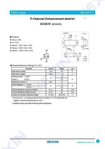
SMD Type IC SMD Type MOSFET P-Channel Enhancement MOSFET AO3419 (KO3419) SOT-23-3 Unit mm +0.2 2.9-0.1 +0.1 0.4 -0.1 Features 3 VDS (V) = -20V ID = -3.5 A RDS(ON) 75m (VGS = -10V) 1 2 +0.02 RDS(ON) 95m (VGS = -4.5V) +0.1 0.15 -0.02 0.95 -0.1 1.9+0.1 -0.2 D RDS(ON) 145m (VGS = -2.5V) 1. Gate 2. Source G 3. Drain S Absolute Maximum Ratings Ta = 25 Parameter Symbol R
ao3415 ko3415.pdf
SMD Type MOSFET P-Channel MOSFET AO3415 (KO3415) SOT-23-3 Unit mm +0.2 2.9-0.1 +0.1 0.4 -0.1 Features 3 VDS (V) =-20V ID =-5 A (VGS =-4.5V) RDS(ON) 43m (VGS =-4.5V) 1 2 RDS(ON) 55m (VGS =-2.5V) +0.02 +0.1 0.15 -0.02 0.95 -0.1 +0.1 1.9-0.2 RDS(ON) 75m (VGS =-1.8V) RDS(ON) 100m (VGS =-1.5V) 1. Gate D 2. Source 3
ao3415as.pdf
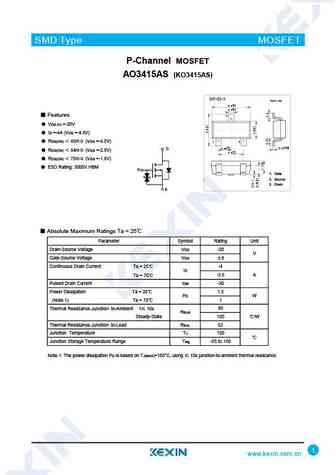
SMD Type MOSFET P-Channel MOSFET AO3415AS (KO3415AS) SOT-23-3 Unit mm +0.2 2.9 -0.1 +0.1 0.4-0.1 Features 3 VDS (V) =-20V ID =-4A (VGS =-4.5V) RDS(ON) 45m (VGS =-4.5V) 1 2 +0.02 +0.1 0.15 -0.02 0.95 -0.1 D RDS(ON) 54m (VGS =-2.5V) +0.1 1.9 -0.2 RDS(ON) 75m (VGS =-1.8V) ESD Rating 3000V HBM G 1. Gate 2. Source 3. Dra
ao3414-3.pdf
SMD Type IC SMD Type MOSFET N-Channel Enhancement MOSFET AO3414 (KO3414) SOT-23-3 Unit mm +0.2 2.9-0.1 Features +0.1 0.4 -0.1 3 VDS (V) = 20V ID = 4.2A (VGS=4.5V) RDS(ON) 50m (VGS = 4.5V) 1 2 RDS(ON) 63m (VGS = 2.5V) +0.02 D +0.1 0.15 -0.02 0.95 -0.1 RDS(ON) 87m (VGS = 1.8V) +0.1 1.9-0.2 1. Gate G 2. Source S 3. Drain Absolute Maximum Ratings Ta = 25 Parameter Sym
ao3410-3.pdf
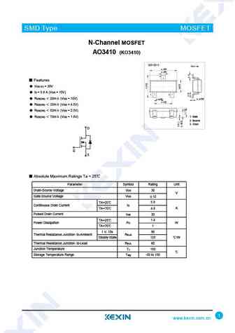
SMD Type MOSFET N-Channel MOSFET AO3410 (KO3410) SOT-23-3 Unit mm +0.2 2.9 -0.1 +0.1 0.4-0.1 3 Features VDS (V) = 30V ID = 5.8 A (VGS = 10V) 1 2 +0.02 +0.1 RDS(ON) 28m (VGS = 10V) 0.15 -0.02 0.95 -0.1 +0.1 1.9 -0.2 RDS(ON) 33m (VGS = 4.5V) RDS(ON) 52m (VGS = 2.5V) 1. Gate RDS(ON) 70m (VGS = 1.8V) 2. Source 3. Dr
ao3419.pdf
SMD Type IC SMD Type MOSFET P-Channel Enhancement MOSFET AO3419 (KO3419) SOT-23 Unit mm +0.1 2.9 -0.1 Features +0.1 0.4 -0.1 VDS (V) = -20V 3 ID = -3.5 A RDS(ON) 75m (VGS = -10V) 1 2 RDS(ON) 95m (VGS = -4.5V) +0.1 +0.05 0.95 -0.1 0.1 -0.01 +0.1 1.9 -0.1 RDS(ON) 145m (VGS = -2.5V) 1.Base 1. Gate 2.Emitter 2. Source 3. Drain 3.collector Absolute Maximum Ratings Ta =
ao3415-3.pdf

SMD Type MOSFET P-Channel MOSFET AO3415 (KO3415) SOT-23-3 Unit mm +0.2 2.9-0.1 +0.1 0.4 -0.1 Features 3 VDS (V) =-20V ID =-5 A (VGS =-4.5V) RDS(ON) 43m (VGS =-4.5V) 1 2 RDS(ON) 55m (VGS =-2.5V) +0.02 +0.1 0.15 -0.02 0.95 -0.1 +0.1 1.9-0.2 RDS(ON) 75m (VGS =-1.8V) RDS(ON) 100m (VGS =-1.5V) 1. Gate D 2. Source 3
ao3415a-3.pdf
SMD Type MOSFET P-Channel MOSFET AO3415A (KO3415A) SOT-23-3 Unit mm +0.2 2.9 -0.1 +0.1 0.4 -0.1 3 Features VDS (V) =-20V ID =-5 A (VGS =-4.5V) 1 2 RDS(ON) 43m (VGS =-4.5V) +0.02 +0.1 0.15 -0.02 0.95 -0.1 +0.1 1.9 -0.2 RDS(ON) 55m (VGS =-2.5V) RDS(ON) 75m (VGS =-1.8V) RDS(ON) 100m (VGS =-1.5V) 1. Gate 2. Source
ao3413a.pdf
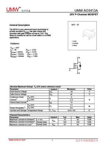
R UMW UMW AO3413A 20V P-Channel MOSFET SOT 23 General Description General Description The AO3413 uses advanced trench technology to The AO3413 uses advanced trench technology to provide excellent RDS(ON), low gate charge and provide excellent RDS(ON), low gate charge and operation with gate voltages as low as 1.8V. This operation with gate voltages as low as 1.8V. This device
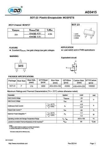
ao3415a.pdf
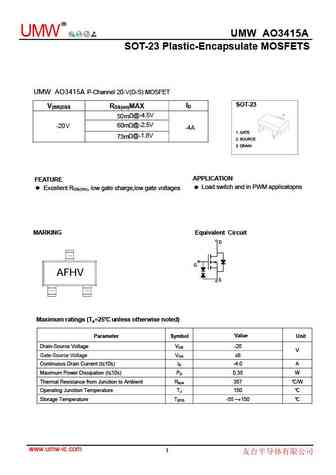
R UMW UMW AO3415A SOT-23 Plastic-Encapsulate MOSFETS UMW AO3415A P-Channel 20-V(D-S) MOSFET SOT-23 ID V(BR)DSS RDS(on)MAX 50m @-4.5V -20V 60m @-2.5V -4A 1. GATE 73m @-1.8V 2. SOURCE 3. DRAIN APPLICATION FEATURE Load switch and in PWM applicatopns Excellent RDS(ON), low gate charge,low gate voltages MARKING Equivalent Circuit D G AFHV S Maximum ratings
ao3414a.pdf
R UMW UMW AO3414A UMW AO3414A N-Channel Enhancement MOSFET Features VDS (V) = 20V SOT 23 ID = 4.2A (VGS=4.5V) RDS(ON) 50m (VGS = 4.5V) RDS(ON) 63m (VGS = 2.5V) RDS(ON) 87m (VGS = 1.8V) MARKING 1. GATE 2. SOURCE 3. DRAIN Absolute Maximum Ratings Ta = 25 Parameter Symbol Rating Unit Drain-Source Voltage VDS 20 V Gate-Source Voltage VGS 8 V Continuous Drain TA=25 4.2 ID
ao3416a.pdf
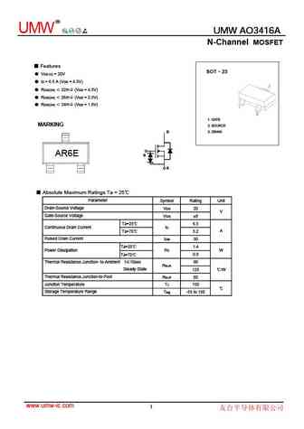
R UMW UMW AO3416A UMW AO3416A N-Channel MOSFET Features SOT 23 VDS (V) = 20V ID = 6.5 A (VGS = 4.5V) RDS(ON) 22m (VGS = 4.5V) RDS(ON) 26m (VGS = 2.5V) RDS(ON) 34m (VGS = 1.8V) 1. GATE MARKING 2. SOURCE D D 3. DRAIN AR6E G G S S Absolute Maximum Ratings Ta = 25 Parameter Symbol Rating Unit Drain-Source Voltage VDS 20
ao3415.pdf
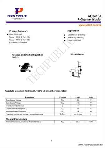
Plastic-Encapsulate Mosfets AO3415 FEATURES P-Channel MOSFET The AO3415 uses advanced trench technology to provide excellent RDS(ON), low gate charge and operation with gate voltages as low as 1.8V. This device is suitable for use as a load switch applications. D 1.Gate 2.Source SOT-23 3.Drain G S Absolute Maximum Ratings (TA=25oC, unless otherwise noted) Parameter Symbol Maxim
ao3415.pdf
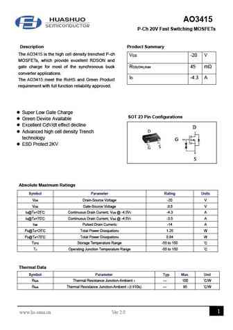
AO3415 P-Ch 20V Fast Switching MOSFETs Description Product Summary The AO3415 is the high cell density trenched P-ch VDS -20 V MOSFETs, which provide excellent RDSON and gate charge for most of the synchronous buck RDS(ON),max 45 m converter applications. ID -4.3 A The AO3415 meet the RoHS and Green Product requirement with full function reliability approved. Super L
ao3415.pdf
AO3415 SOT-23 Plastic-Encapsulate MOSFETS SOT-23 20V P-Channel MOSFET 3 ID Max V(BR)DSS RDS(on)Typ 37m @ -4.5V 1. GATE -4.8A -20V 2. SOURCE 43m @ -3.3V 1 3. DRAIN 2 APPLICATION FEATURE Load switch and in PWM applicatopns Excellent RDS(ON), low gate charge,low gate voltages MARKING Equivalent circuit D 3415 G S PACKAGE SPECIFICATIONS Reel DI
ao3415ai-ms.pdf
www.msksemi.com AO3415AI-MS Semiconductor Compiance D VDS -20V I (at V =-4.5V) -4A D GS R (at V = -4.5V)
ao3415.pdf
AO3415 -20V P-Channel Enhancement Mode MOSFET General Features Description VDS = -20V,ID =-4A The AO3415 uses advanced trench technology to provide RDS(ON)
ao3416.pdf
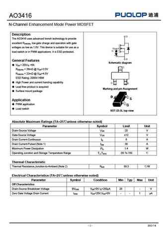
AO3416 N-Channel Enhancement Mode Power MOSFET Description The AO3416 uses advanced trench technology to provide excellent RDS(ON), low gate charge and operation with gate voltages as low as 1.8V. This device is suitable for use as a load switch or in PWM applications .It is ESD protested. General Features Schematic diagram VDS = 20V,ID =6A RDS(ON)
ao3413.pdf
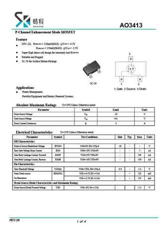
AO3413 P-Channel Enhancement Mode MOSFET Feature DS(ON) GS -20V/-3A, R = 120m (MAX) @V = -4.5V. DS(ON) GS R = 150m (MAX) @V = -2.5V. DS(ON) Super High dense cell design for extremely low R 3 Reliable and Rugged SC-59 for Surface Mount Package SC-59 1 2 Applications 1 Gate 2 Source 3 Drain Power Management Portable Equipment and Battery Powered Sy
ao3416.pdf
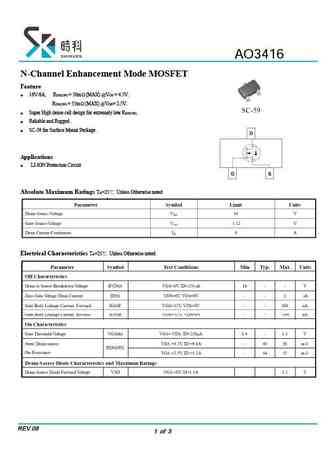
AO3416 N-Channel Enhancement Mode MOSFET Feature 16V/6A, RDS(ON) = 50m (MAX) @VGS = 4.5V. RDS(ON) = 55m (MAX) @VGS= 2.5V. Super High dense cell design for extremely low RDS(ON) . Reliable and Rugged . SC-59 for Surface Mount Package . Applications LI-ION Protection Circuit Absolute Maximum Ratings TA=25 Unless Otherwise noted Electrical Characteris
ao3414.pdf
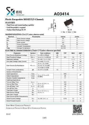
Plastic-Encapsulate MOSFET(N Encapsulate MOSFET(N-Channel) FEATURES High Power and current handing capability High Power and current handing capability Lead free product is acquired Surface Mout Package SC-59 SC-59 1 Gate 2 3 Drain Gate 2 Source MAXIMUM RATINGS (TA=25 unless otherwise noted) unless otherwise noted) ELECTRICAL CHARACTERISTICS (Tamb=25 unless
ao3415.pdf
SHENZHEN LONG JING MICRO-ELECTRONICS CO., LTD. SOT-23 Plastic-Encapsulate Mosfets AO3415 20V P-Channel Mosfet Features V = -20V DS I = 3A (V = -4V) D GS R
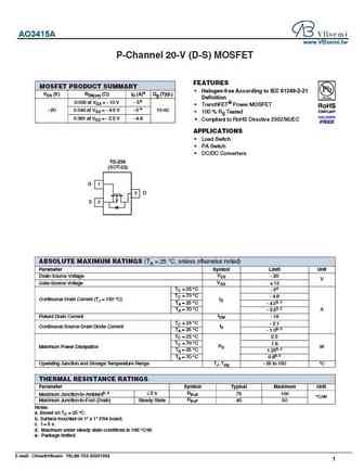
ao3414.pdf
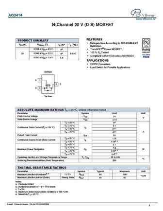
AO3414 www.VBsemi.tw N-Channel 20 V (D-S) MOSFET FEATURES PRODUCT SUMMARY Halogen-free According to IEC 61249-2-21 VDS (V) RDS(on) ( ) ID (A)e Qg (Typ.) Definition 0.028 at VGS = 4.5 V TrenchFET Power MOSFET 6a 100 % Rg Tested 20 0.042 at VGS = 2.5 V 6a 8.8 nC Compliant to RoHS Directive 2002/95/EC 0.050 at VGS = 1.8 V 5.6 APPLICATIONS DC/DC Convert
Другие IGBT... AO3406, AO3407A, AO3409, AO3413, AO3414, AO3415, AO3415A, AO3416, STP65NF06, AO3419, AO3420, AO3421, AO3421E, AO3422, AO3423, AO3424, AO3434
🌐 : EN ES РУ

Список транзисторов
Обновления
MOSFET: AUP060N055 | AUP056N10 | AUP056N08BGL | AUP052N085 | AUP045N12 | AUP039N10 | AUP034N10 | AUP034N06 | AUP033N08BG | AUP026N085 | AUN084N10 | AUN065N10 | AUN063N10 | AUN062N08BG | AUN060N08AG | AUN053N10
Popular searches
tip127 datasheet | irlz24n | irf620 | irfp350 | 13003 transistor | c458 transistor | 2sc1775 | 2n1305