AO4446. Аналоги и основные параметры
Наименование производителя: AO4446
Тип транзистора: MOSFET
Полярность: N
Предельные значения
Pd ⓘ
- Максимальная рассеиваемая мощность: 3 W
|Vds|ⓘ - Максимально допустимое напряжение сток-исток: 30 V
|Vgs|ⓘ - Максимально допустимое напряжение затвор-исток: 20 V
|Id| ⓘ - Максимально допустимый постоянный ток стока: 15 A
Tj ⓘ - Максимальная температура канала: 150 °C
Электрические характеристики
tr ⓘ -
Время нарастания: 8.2 ns
Cossⓘ - Выходная емкость: 306 pf
RDSonⓘ - Сопротивление сток-исток открытого транзистора: 0.0085 Ohm
Тип корпуса: SO-8
Аналог (замена) для AO4446
- подборⓘ MOSFET транзистора по параметрам
AO4446 даташит
..1. Size:166K aosemi
ao4446.pdf 
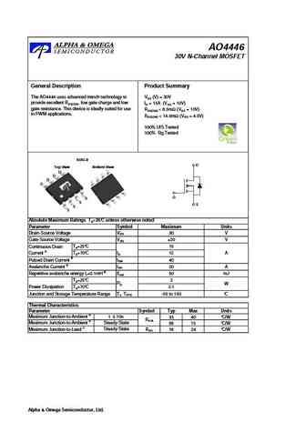
AO4446 30V N-Channel MOSFET General Description Product Summary The AO4446 uses advanced trench technology to VDS (V) = 30V provide excellent RDS(ON), low gate charge and low ID = 15A (VGS = 10V) gate resistance. This device is ideally suited for use RDS(ON)
..2. Size:1386K kexin
ao4446.pdf 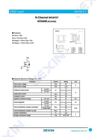
SMD Type MOSFET N-Channel MOSFET AO4446 (KO4446) SOP-8 Features VDS (V) = 30V ID = 15 A (VGS = 10V) RDS(ON) 8.5m (VGS = 10V) 1.50 0.15 RDS(ON) 14.5m (VGS = 4.5V) 1 Source 5 Drain 6 Drain 2 Source 7 Drain 3 Source 8 Drain 4 Gate D G S Absolute Maximum Ratings Ta = 25 Parameter Symbol Rating Unit Drain-Source Voltage VDS 30 V Ga
..3. Size:833K cn vbsemi
ao4446.pdf 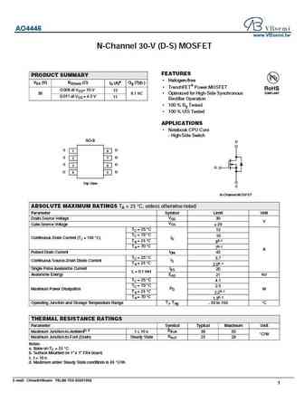
AO4446 www.VBsemi.tw N-Channel 30-V (D-S) MOSFET FEATURES PRODUCT SUMMARY Halogen-free VDS (V) RDS(on) ( ) ID (A)a Qg (Typ.) TrenchFET Power MOSFET 0.008 at VGS = 10 V 13 30 6.1 nC Optimized for High-Side Synchronous 0.011 at VGS = 4.5 V 11 Rectifier Operation 100 % Rg Tested 100 % UIS Tested APPLICATIONS Notebook CPU Core - High-Side Switch SO
9.1. Size:302K aosemi
ao4441.pdf 
AO4441 60V P-Channel MOSFET General Description Product Summary VDS The AO4441 uses advanced trench technology to provide -60V excellent RDS(ON), and ultra-low low gate charge. This ID (at VGS=-10V) -4A device is suitable for use as a load switch or in PWM RDS(ON) (at VGS=-10V)
9.2. Size:167K aosemi
ao4440.pdf 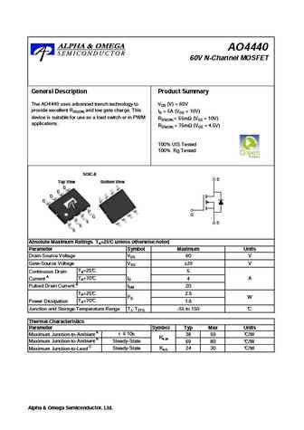
AO4440 60V N-Channel MOSFET General Description Product Summary The AO4440 uses advanced trench technology to VDS (V) = 60V provide excellent RDS(ON) and low gate charge. This ID = 5A (VGS = 10V) device is suitable for use as a load switch or in PWM RDS(ON)
9.3. Size:286K aosemi
ao4448.pdf 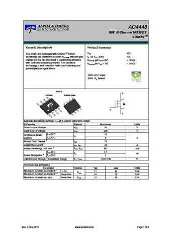
AO4448 80V N-Channel MOSFET TM SDMOS General Description Product Summary VDS 80V The AO4448 is fabricated with SDMOSTM trench ID (at VGS=10V) 10A technology that combines excellent RDS(ON) with low gate charge and low Qrr.The result is outstanding efficiency RDS(ON) (at VGS=10V)
9.4. Size:246K aosemi
ao4442.pdf 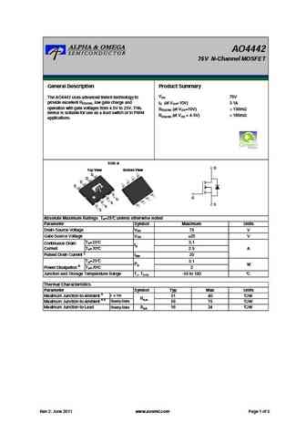
AO4442 75V N-Channel MOSFET General Description Product Summary VDS 75V The AO4442 uses advanced trench technology to provide excellent RDS(ON), low gate charge and ID (at VGS=10V) 3.1A operation with gate voltages from 4.5V to 25V. This RDS(ON) (at VGS=10V)
9.5. Size:609K aosemi
ao4449.pdf 
AO4449 30V P-Channel MOSFET General Description Product Summary VDS -30V The AO4449 uses advanced trench technology to provide excellent RDS(ON), and ultra-low low gate charge. This ID (at VGS=-10V) -7A device is suitable for use as a load switch or in PWM RDS(ON) (at VGS=-10V)
9.6. Size:308K aosemi
ao4443.pdf 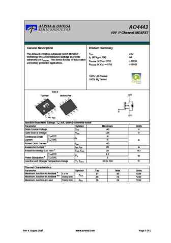
AO4443 40V P-Channel MOSFET General Description Product Summary VDS -40V The AO4443 combines advanced trench MOSFET technology with a low resistance package to provide ID (at VGS=-10V) -6A extremely low RDS(ON). This device is ideal for load switch RDS(ON) (at VGS=-10V)
9.7. Size:279K aosemi
ao4444l.pdf 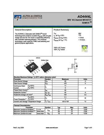
AO4444L 80V N-Channel MOSFET TM SDMOS General Description Product Summary VDS 80V The AO4444L is fabricated with SDMOSTM trench 11A ID (at VGS=10V) technology that combines excellent RDS(ON) with low gate
9.8. Size:169K aosemi
ao4447.pdf 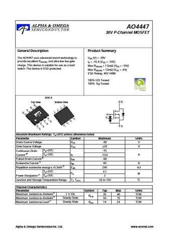
AO4447 30V P-Channel MOSFET General Description Product Summary The AO4447 uses advanced trench technology to VDS (V) = -30V provide excellent RDS(ON), and ultra-low low gate ID = -15 A (VGS = -10V) charge. This device is suitable for use as a load Max RDS(ON)
9.9. Size:302K aosemi
ao4447a.pdf 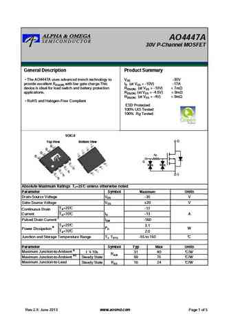
AO4447A 30V P-Channel MOSFET General Description Product Summary The AO4447A uses advanced trench technology to VDS -30V provide excellent RDS(ON) with low gate charge.This ID (at VGS = -10V) -17A device is ideal for load switch and battery protection RDS(ON) (at VGS = -10V)
9.10. Size:1248K kexin
ao4441.pdf 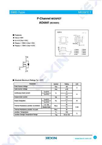
SMD Type MOSFET P-Channel MOSFET AO4441 (KO4441) SOP-8 Features VDS (V) =-60V ID =-4 A (VGS =-10V) RDS(ON) 100m (VGS =-10V) 1.50 0.15 RDS(ON) 130m (VGS =-4.5V) 1 Source 5 Drain 6 Drain 2 Source 7 Drain 3 Source 8 Drain 4 Gate D G S Absolute Maximum Ratings Ta = 25 Parameter Symbol Rating Unit Drain-Source Voltage VDS -60 V Gat
9.11. Size:1234K kexin
ao4440.pdf 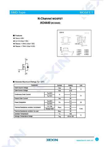
SMD Type MOSFET N-Channel MOSFET AO4440 (KO4440) SOP-8 Features VDS (V) = 60V ID = 5 A (VGS = 10V) RDS(ON) 55m (VGS = 10V) 1.50 0.15 RDS(ON) 75m (VGS = 4.5V) 1 Source 5 Drain 6 Drain 2 Source 7 Drain 3 Source 8 Drain 4 Gate D G S Absolute Maximum Ratings Ta = 25 Parameter Symbol Rating Unit Drain-Source Voltage VDS 60 V Gate-So
9.12. Size:1559K kexin
ao4448.pdf 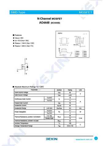
SMD Type MOSFET N-Channel MOSFET AO4448 (KO4448) SOP-8 Features VDS (V) = 80V ID = 10 A (VGS = 10V) RDS(ON) 16m (VGS = 10V) 1.50 0.15 RDS(ON) 20m (VGS = 7V) 1 Source 5 Drain 6 Drain 2 Source 7 Drain 3 Source 8 Drain 4 Gate D G S Absolute Maximum Ratings Ta = 25 Parameter Symbol Rating Unit Drain-Source Voltage VDS 80 V Gate-So
9.13. Size:1264K kexin
ao4442.pdf 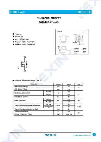
SMD Type MOSFET N-Channel MOSFET AO4442 (KO4442) SOP-8 Features VDS (V) = 75V ID = 3.1 A (VGS = 10V) RDS(ON) 130m (VGS = 10V) 1.50 0.15 RDS(ON) 165m (VGS = 4.5V) 1 Source 5 Drain 6 Drain 2 Source 7 Drain 3 Source 8 Drain 4 Gate D G S Absolute Maximum Ratings Ta = 25 Parameter Symbol Rating Unit Drain-Source Voltage VDS 75 V Ga
9.14. Size:2066K kexin
ao4449.pdf 
SMD Type MOSFET P-Channel MOSFET AO4449 (KO4449) SOP-8 Features VDS (V) =-30V ID =-7 A (VGS =-10V) RDS(ON) 34m (VGS =-10V) 1.50 0.15 RDS(ON) 54m (VGS =-4.5V) 1 Source 5 Drain 6 Drain 2 Source 7 Drain 3 Source 8 Drain 4 Gate D D G G S S Absolute Maximum Ratings Ta = 25 Parameter Symbol Rating Unit Drain-Source Voltage VDS -30
9.15. Size:1234K kexin
ao4443.pdf 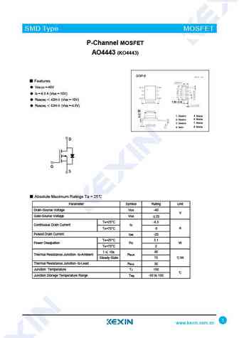
SMD Type MOSFET P-Channel MOSFET AO4443 (KO4443) SOP-8 Features VDS (V) =-40V ID =-6.5 A (VGS =-10V) RDS(ON) 42m (VGS =-10V) 1.50 0.15 RDS(ON) 63m (VGS =-4.5V) 1 Source 5 Drain 6 Drain 2 Source 7 Drain 3 Source 8 Drain 4 Gate D G S Absolute Maximum Ratings Ta = 25 Parameter Symbol Rating Unit Drain-Source Voltage VDS -40 V Gat
9.16. Size:1251K kexin
ao4444.pdf 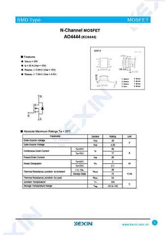
SMD Type MOSFET N-Channel MOSFET AO4444 (KO4444) SOP-8 Features VDS (V) = 30V ID = 20 A (VGS = 10V) 1.50 0.15 RDS(ON) 5.5m (VGS = 10V) RDS(ON) 7.5m (VGS = 4.5V) 1 Source 5 Drain 6 Drain 2 Source 7 Drain 3 Source 8 Drain 4 Gate D G S Absolute Maximum Ratings Ta = 25 Parameter Symbol Rating Unit Drain-Source Voltage VDS 30 V Gat
9.17. Size:1526K kexin
ao4447.pdf 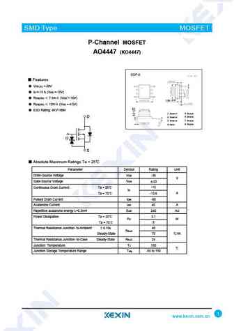
SMD Type MOSFET P-Channel MOSFET AO4447 (KO4447) SOP-8 Features VDS (V) =-30V ID =-15 A (VGS =-10V) RDS(ON) 7.5m (VGS =-10V) 1.50 0.15 RDS(ON) 12m (VGS =-4.5V) ESD Rating 4KV HBM 1 Source 5 Drain 6 Drain D 2 Source 7 Drain 3 Source 8 Drain 4 Gate G S Absolute Maximum Ratings Ta = 25 Parameter Symbol Rating Unit Drain-Source
9.18. Size:1685K kexin
ao4447a.pdf 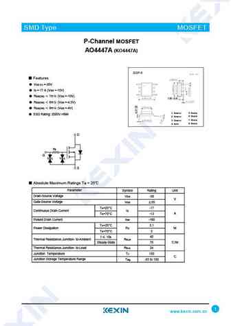
SMD Type MOSFET P-Channel MOSFET AO4447A (KO4447A) SOP-8 Features VDS (V) =-30V ID =-17 A (VGS =-10V) RDS(ON) 7m (VGS =-10V) 1.50 0.15 RDS(ON) 8m (VGS =-4.5V) RDS(ON) 9m (VGS =-4V) 1 Source 5 Drain ESD Rating 2000V HBM 6 Drain 2 Source 7 Drain 3 Source 8 Drain 4 Gate D Rg G S Absolute Maximum Ratings Ta = 25 Par
9.19. Size:881K cn vbsemi
ao4441.pdf 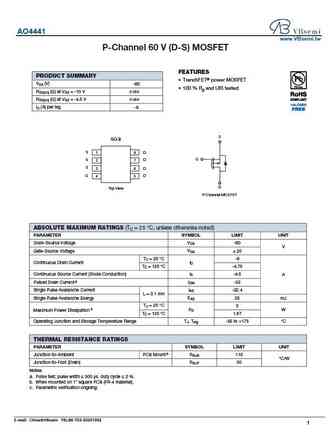
AO4441 www.VBsemi.tw P-Channel 60 V (D-S) MOSFET FEATURES PRODUCT SUMMARY TrenchFET power MOSFET VDS (V) -60 100 % Rg and UIS tested RDS(on) ( ) at VGS = -10 V 0.050 RDS(on) ( ) at VGS = -4.5 V 0.060 ID (A) per leg -8 S SO-8 S 1 8 D G S D 2 7 S 3 6 D G D 4 5 D Top View P-Channel MOSFET ABSOLUTE MAXIMUM RATINGS (TC = 25 C, unless otherwise noted) PARAMETER
9.20. Size:803K cn vbsemi
ao4449.pdf 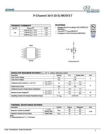
AO4449 www.VBsemi.tw P-Channel 30-V (D-S) MOSFET FEATURES PRODUCT SUMMARY Halogen-free According to IEC 61249-2-21 VDS (V) RDS(on) ( )ID (A) Definition 0.042 at VGS = - 10 V - 5.8 TrenchFET Power MOSFET 0.055 at VGS = - 6 V - 30 - 5.0 Compliant to RoHS Directive 2002/95/EC 0.060 at VGS = - 4.5 V - 4.4 S SO-8 G SD 1 8 S D 2 7 3 6 SD G D 4 5 D Top Vi
9.21. Size:1396K cn vbsemi
ao4443.pdf 
AO4443 www.VBsemi.tw P-Channel 30-V (D-S) MOSFET FEATURES PRODUCT SUMMARY Halogen-free According to IEC 61249-2-21 VDS (V) RDS(on) ( )ID (A) Definition 0.042 at VGS = - 10 V - 5.8 TrenchFET Power MOSFET 0.055 at VGS = - 6 V - 30 - 5.0 Compliant to RoHS Directive 2002/95/EC 0.060 at VGS = - 4.5 V - 4.4 S SO-8 G SD 1 8 S D 2 7 3 6 SD G D 4 5 D Top Vi
9.22. Size:821K cn vbsemi
ao4447a.pdf 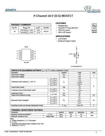
AO4447A www.VBsemi.tw P-Channel 30-V (D-S) MOSFET FEATURES PRODUCT SUMMARY Halogen-free VDS (V) RDS(on) ( ) ID (A)d Qg (Typ.) TrenchFET Power MOSFET 0.011 at VGS = - 10 V - 13.5 100 % Rg Tested RoHS - 30 29.5 nC COMPLIANT 100 % UIS Tested 0.015 at VGS = - 4.5 V - 11.6 APPLICATIONS Load Switch Notebook Adaptor Switch SO-8 S S 1 8 D S D 2 7 G
Другие IGBT... AO4435, AO4437, AO4438, AO4440, AO4441, AO4442, AO4443, AO4444L, IRF4905, AO4447, AO4447A, AO4448, AO4449, AO4450, AO4452, AO4453, AO4454
