APT20M10JLL. Аналоги и основные параметры
Наименование производителя: APT20M10JLL
Тип транзистора: MOSFET
Полярность: N
Предельные значения
Pd ⓘ
- Максимальная рассеиваемая мощность: 690 W
|Vds|ⓘ - Максимально допустимое напряжение сток-исток: 200 V
|Vgs|ⓘ - Максимально допустимое напряжение затвор-исток: 30 V
|Id| ⓘ - Максимально допустимый постоянный ток стока: 180 A
Tj ⓘ - Максимальная температура канала: 150 °C
Электрические характеристики
tr ⓘ -
Время нарастания: 35 ns
Cossⓘ - Выходная емкость: 4330 pf
RDSonⓘ - Сопротивление сток-исток открытого транзистора: 0.01 Ohm
Тип корпуса: SOT227
Аналог (замена) для APT20M10JLL
- подборⓘ MOSFET транзистора по параметрам
APT20M10JLL даташит
..1. Size:61K apt
apt20m10jll 1.pdf 
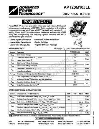
APT20M10JLL 200V 185A 0.010 W TM POWER MOS 7 Power MOS 7TM is a new generation of low loss, high voltage, N-Channel enhancement mode power MOSFETS. Both conduction and switching losses are addressed with Power MOS 7TM by significantly lowering RDS(ON) and Qg. Power MOS 7TM combines lower conduction and switching losses along with exceptionally fast switching speeds inherent with APT's
..2. Size:69K apt
apt20m10jll.pdf 
APT20M10JLL 200V 185A 0.010W TM POWER MOS 7 Power MOS 7TM is a new generation of low loss, high voltage, N-Channel enhancement mode power MOSFETS. Both conduction and switching losses are addressed with Power MOS 7TM by significantly lowering RDS(ON) and Qg. Power MOS 7TM combines lower conduction and switching losses along with exceptionally fast switching speeds inherent with APT's
5.1. Size:63K apt
apt20m10jfll.pdf 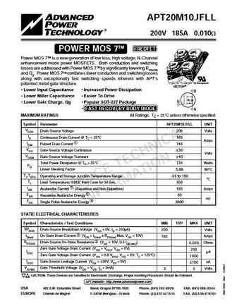
APT20M10JFLL 200V 185A 0.010W TM FREDFET POWER MOS 7 Power MOS 7TM is a new generation of low loss, high voltage, N-Channel enhancement mode power MOSFETS. Both conduction and switching losses are addressed with Power MOS 7TM by significantly lowering RDS(ON) and Qg. Power MOS 7TM combines lower conduction and switching losses along with exceptionally fast switching speeds inherent wi
7.1. Size:159K apt
apt20m18b2vrg apt20m18lvrg.pdf 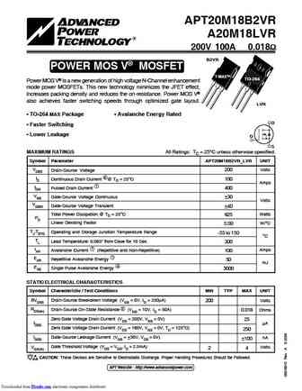
APT20M18B2VR A20M18LVR 200V 100A 0.018 B2VR POWER MOS V MOSFET T-MAX TO-264 Power MOS V is a new generation of high voltage N-Channel enhancement mode power MOSFETs. This new technology minimizes the JFET effect, increases packing density and reduces the on-resistance. Power MOS V also achieves faster switching speeds through optimized gate layout. LV
7.2. Size:152K apt
apt20m18b2vfrg apt20m18lvfrg.pdf 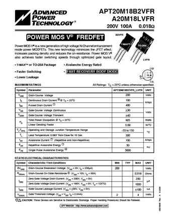
APT20M18B2VFR A20M18LVFR 200V 100A 0.018 B2VFR POWER MOS V FREDFET T-MAX TO-264 Power MOS V is a new generation of high voltage N-Channel enhancement mode power MOSFETs. This new technology minimizes the JFET effect, increases packing density and reduces the on-resistance. Power MOS V also achieves faster switching speeds through optimized gate layout.
7.3. Size:39K apt
apt20m18b2vfr.pdf 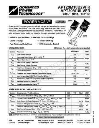
APT20M18B2VFR APT20M18LVFR 200V 100A 0.018W B2VFR POWER MOS V FREDFET T-MAX Power MOS V is a new generation of high voltage N-Channel enhancement TO-264 mode power MOSFETs. This new technology minimizes the JFET effect, increases packing density and reduces the on-resistance. Power MOS V also achieves faster switching speeds through optimized gate layout. LVFR Identical
7.4. Size:70K apt
apt20m16b2ll.pdf 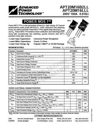
APT20M16B2LL APT20M16LLL 200V 100A 0.016W B2LL TM POWER MOS 7 Power MOS 7TM is a new generation of low loss, high voltage, N-Channel T-MAX TO-264 enhancement mode power MOSFETS. Both conduction and switching losses are addressed with Power MOS 7TM by significantly lowering RDS(ON) and Qg. Power MOS 7TM combines lower conduction and switching losses along with exceptionally fast
7.5. Size:166K apt
apt20m11jll.pdf 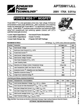
APT20M11JLL 200V 176A 0.011 R POWER MOS 7 MOSFET Power MOS 7 is a new generation of low loss, high voltage, N-Channel enhancement mode power MOSFETS. Both conduction and switching losses are addressed with Power MOS 7 by significantly lowering RDS(ON) and Qg. Power MOS 7 combines lower conduction and switching losses "UL Recognized" along with exceptionall
7.6. Size:74K apt
apt20m11jvfr.pdf 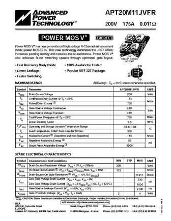
APT20M11JVFR 200V 175A 0.011 POWER MOS V FREDFET Power MOS V is a new generation of high voltage N-Channel enhancement mode power MOSFETs. This new technology minimizes the JFET effect, increases packing density and reduces the on-resistance. Power MOS V also achieves faster switching speeds through optimized gate layout. ISOTOP Fast Recovery Body Diode 100% Avalanche
7.7. Size:171K apt
apt20m16b2llg apt20m16lllg.pdf 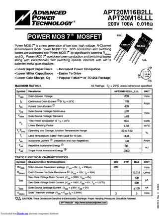
APT20M16B2LL APT20M16LLL 200V 100A 0.016 R B2LL POWER MOS 7 MOSFET T-MAX Power MOS 7 is a new generation of low loss, high voltage, N-Channel TO-264 enhancement mode power MOSFETS. Both conduction and switching losses are addressed with Power MOS 7 by significantly lowering RDS(ON) and Qg. Power MOS 7 combines lower conduction and switching losses LL
7.8. Size:38K apt
apt20m18b2vr.pdf 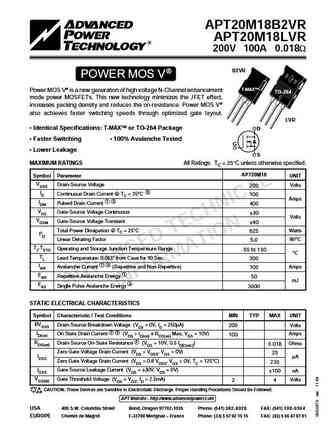
APT20M18B2VR APT20M18LVR 200V 100A 0.018W B2VR POWER MOS V T-MAX Power MOS V is a new generation of high voltage N-Channel enhancement TO-264 mode power MOSFETs. This new technology minimizes the JFET effect, increases packing density and reduces the on-resistance. Power MOS V also achieves faster switching speeds through optimized gate layout. LVR Identical Specificati
7.9. Size:36K apt
apt20m13pvr.pdf 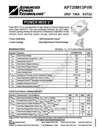
APT20M13PVR 200V 146A 0.013 POWER MOS V P-Pack Power MOS V is a new generation of high voltage N-Channel enhancement mode power MOSFETs. This new technology minimizes the JFET effect, increases packing density and reduces the on-resistance. Power MOS V also achieves faster switching speeds through optimized gate layout. Faster Switching 100% Avalanche Tested D Lowe
7.10. Size:74K apt
apt20m11jvr.pdf 
APT20M11JVR 200V 175A 0.011 POWER MOS V Power MOS V is a new generation of high voltage N-Channel enhancement mode power MOSFETs. This new technology minimizes the JFET effect, increases packing density and reduces the on-resistance. Power MOS V also achieves faster switching speeds through optimized gate layout. "UL Recognized" ISOTOP Faster Switching 100% Avalanche
7.11. Size:162K apt
apt20m16b2fllg apt20m16lfllg.pdf 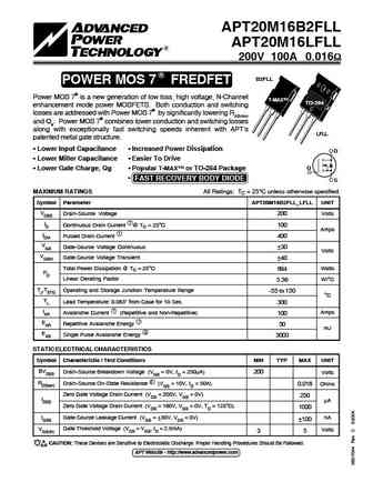
APT20M16B2FLL APT20M16LFLL 200V 100A 0.016 R B2FLL POWER MOS 7 FREDFET Power MOS 7 is a new generation of low loss, high voltage, N-Channel T-MAX TO-264 enhancement mode power MOSFETS. Both conduction and switching losses are addressed with Power MOS 7 by significantly lowering RDS(ON) and Qg. Power MOS 7 combines lower conduction and switching losses
7.12. Size:74K apt
apt20m19jvr.pdf 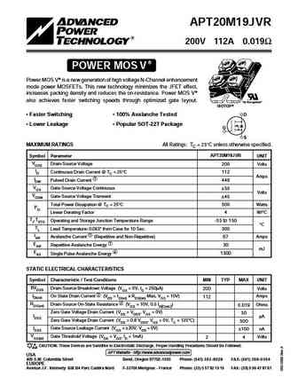
APT20M19JVR 200V 112A 0.019 POWER MOS V Power MOS V is a new generation of high voltage N-Channel enhancement mode power MOSFETs. This new technology minimizes the JFET effect, increases packing density and reduces the on-resistance. Power MOS V also achieves faster switching speeds through optimized gate layout. "UL Recognized" ISOTOP Faster Switching 100% Avalanche
7.13. Size:167K apt
apt20m11jfll.pdf 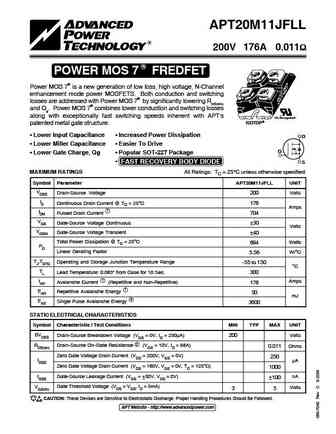
APT20M11JFLL 200V 176A 0.011 R POWER MOS 7 FREDFET Power MOS 7 is a new generation of low loss, high voltage, N-Channel enhancement mode power MOSFETS. Both conduction and switching losses are addressed with Power MOS 7 by significantly lowering RDS(ON) and Qg. Power MOS 7 combines lower conduction and switching losses along with exceptionally fast switchin
7.14. Size:71K apt
apt20m16b2fll.pdf 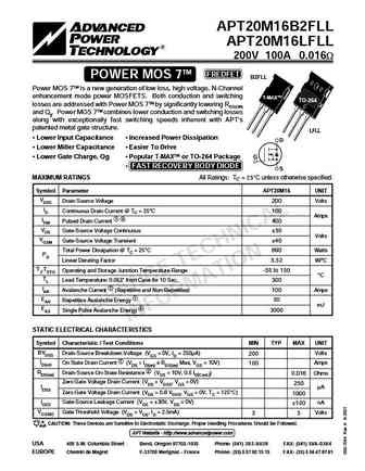
APT20M16B2FLL APT20M16LFLL 200V 100A 0.016W TM FREDFET POWER MOS 7 B2FLL Power MOS 7TM is a new generation of low loss, high voltage, N-Channel enhancement mode power MOSFETS. Both conduction and switching T-MAX TO-264 losses are addressed with Power MOS 7TM by significantly lowering RDS(ON) and Qg. Power MOS 7TM combines lower conduction and switching losses along with excepti
7.15. Size:107K microsemi
apt20m120jcu3.pdf 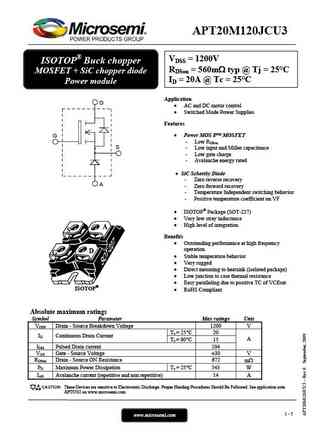
APT20M120JCU3 VDSS = 1200V ISOTOP Buck chopper RDSon = 560m typ @ Tj = 25 C MOSFET + SiC chopper diode ID = 20A @ Tc = 25 C Power module Application D AC and DC motor control Switched Mode Power Supplies Features Power MOS 8 MOSFET G - Low RDSon S - Low input and Miller capacitance - Low gate charge - Avalanche energy rated SiC Schott
7.16. Size:106K microsemi
apt20m120jcu2.pdf 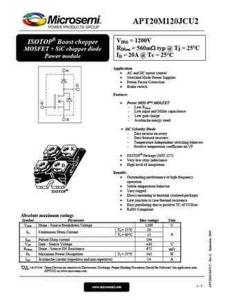
APT20M120JCU2 VDSS = 1200V ISOTOP Boost chopper RDSon = 560m typ @ Tj = 25 C MOSFET + SiC chopper diode ID = 20A @ Tc = 25 C Power module Application K AC and DC motor control Switched Mode Power Supplies Power Factor Correction D Brake switch Features Power MOS 8 MOSFET G - Low RDSon - Low input and Miller capacitance - Low gat
7.17. Size:255K inchange semiconductor
apt20m16lfll.pdf 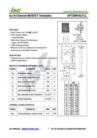
isc N-Channel MOSFET Transistor APT20M16LFLL FEATURES Drain Current I = 100A@ T =25 D C Drain Source Voltage- V =200V(Min) DSS Static Drain-Source On-Resistance R =0.016 (Max) DS(on) 100% avalanche tested Minimum Lot-to-Lot variations for robust device performance and reliable operation DESCRIPTION Designed for use in switch mode power supplies and general
7.18. Size:375K inchange semiconductor
apt20m18b2vfr.pdf 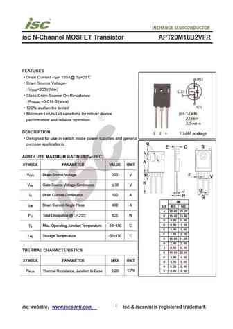
isc N-Channel MOSFET Transistor APT20M18B2VFR FEATURES Drain Current I = 100A@ T =25 D C Drain Source Voltage- V =200V(Min) DSS Static Drain-Source On-Resistance R =0.018 (Max) DS(on) 100% avalanche tested Minimum Lot-to-Lot variations for robust device performance and reliable operation DESCRIPTION Designed for use in switch mode power supplies and general
7.19. Size:376K inchange semiconductor
apt20m16b2ll.pdf 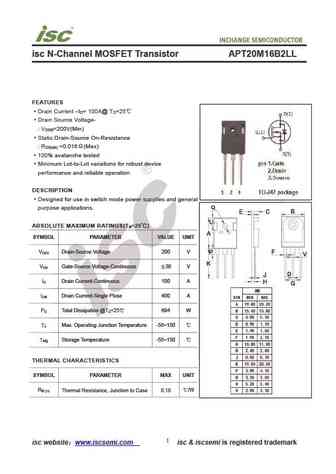
isc N-Channel MOSFET Transistor APT20M16B2LL FEATURES Drain Current I = 100A@ T =25 D C Drain Source Voltage- V =200V(Min) DSS Static Drain-Source On-Resistance R =0.016 (Max) DS(on) 100% avalanche tested Minimum Lot-to-Lot variations for robust device performance and reliable operation DESCRIPTION Designed for use in switch mode power supplies and general
7.20. Size:255K inchange semiconductor
apt20m18lvfr.pdf 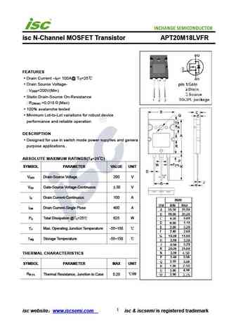
isc N-Channel MOSFET Transistor APT20M18LVFR FEATURES Drain Current I = 100A@ T =25 D C Drain Source Voltage- V =200V(Min) DSS Static Drain-Source On-Resistance R =0.018 (Max) DS(on) 100% avalanche tested Minimum Lot-to-Lot variations for robust device performance and reliable operation DESCRIPTION Designed for use in switch mode power supplies and general
7.21. Size:255K inchange semiconductor
apt20m18lvr.pdf 
isc N-Channel MOSFET Transistor APT20M18LVR FEATURES Drain Current I = 100A@ T =25 D C Drain Source Voltage- V =200V(Min) DSS Static Drain-Source On-Resistance R =0.018 (Max) DS(on) 100% avalanche tested Minimum Lot-to-Lot variations for robust device performance and reliable operation DESCRIPTION Designed for use in switch mode power supplies and general p
7.22. Size:376K inchange semiconductor
apt20m18b2vr.pdf 
isc N-Channel MOSFET Transistor APT20M18B2VR FEATURES Drain Current I = 100A@ T =25 D C Drain Source Voltage- V =200V(Min) DSS Static Drain-Source On-Resistance R =0.018 (Max) DS(on) 100% avalanche tested Minimum Lot-to-Lot variations for robust device performance and reliable operation DESCRIPTION Designed for use in switch mode power supplies and general
7.23. Size:376K inchange semiconductor
apt20m16b2fll.pdf 
isc N-Channel MOSFET Transistor APT20M16B2FLL FEATURES Drain Current I = 100A@ T =25 D C Drain Source Voltage- V =200V(Min) DSS Static Drain-Source On-Resistance R =0.016 (Max) DS(on) 100% avalanche tested Minimum Lot-to-Lot variations for robust device performance and reliable operation DESCRIPTION Designed for use in switch mode power supplies and general
Другие MOSFET... APT12067B2LL
, APT12067JLL
, APT12080B2VFR
, APT12080JVFR
, APT14050JVFR
, APT17N80BC3
, APT17N80SC3
, APT20M10JFLL
, AO3401
, APT20M16B2FLL
, APT20M16B2LL
, APT20M18B2VFR
, APT20M18B2VR
, APT20M20B2FLL
, APT20M20B2LL
, APT20M20JFLL
, APT20M20JLL
.
History: CS20N65P
