APT20N60BC3. Аналоги и основные параметры
Наименование производителя: APT20N60BC3
Тип транзистора: MOSFET
Полярность: N
Предельные значения
Pd ⓘ - Максимальная рассеиваемая мощность: 208 W
|Vds|ⓘ - Максимально допустимое напряжение сток-исток: 600 V
|Vgs|ⓘ - Максимально допустимое напряжение затвор-исток: 20 V
|Id| ⓘ - Максимально допустимый постоянный ток стока: 20.7 A
Tj ⓘ - Максимальная температура канала: 150 °C
Электрические характеристики
tr ⓘ - Время нарастания: 5 ns
Cossⓘ - Выходная емкость: 860 pf
RDSonⓘ - Сопротивление сток-исток открытого транзистора: 0.19 Ohm
Тип корпуса: TO247
Аналог (замена) для APT20N60BC3
- подборⓘ MOSFET транзистора по параметрам
APT20N60BC3 даташит
apt20n60bc3.pdf
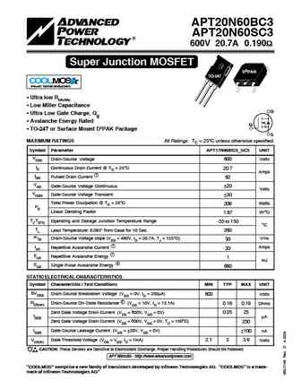
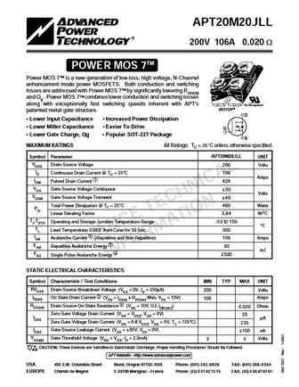
APT20N60BC3 APT20N60SC3 600V 20.7A 0.190 Super Junction MOSFET D3PAK TO-247 COOLMOS Power Semiconductors Ultra low RDS(ON) Low Miller Capacitance D Ultra Low Gate Charge, Qg Avalanche Energy Rated G TO-247 or Surface Mount D3PAK Package S MAXIMUM RATINGS All Ratings TC = 25 C unless otherwise specified. Symbol Parameter APT17N80BC3_S
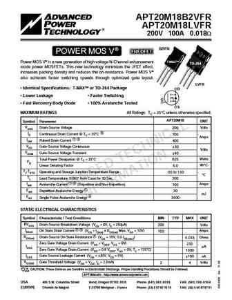
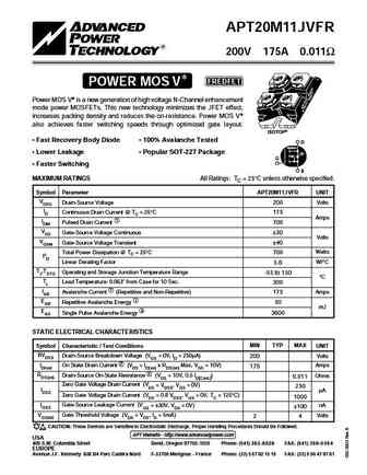
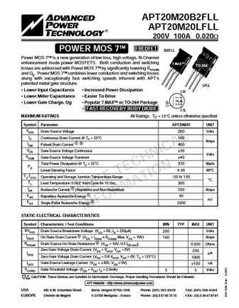
apt20m18b2vrg apt20m18lvrg.pdf
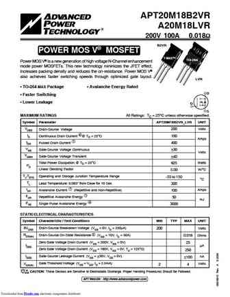
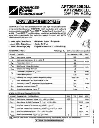
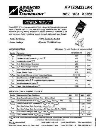
APT20M18B2VR A20M18LVR 200V 100A 0.018 B2VR POWER MOS V MOSFET T-MAX TO-264 Power MOS V is a new generation of high voltage N-Channel enhancement mode power MOSFETs. This new technology minimizes the JFET effect, increases packing density and reduces the on-resistance. Power MOS V also achieves faster switching speeds through optimized gate layout. LV
apt20m18b2vfrg apt20m18lvfrg.pdf
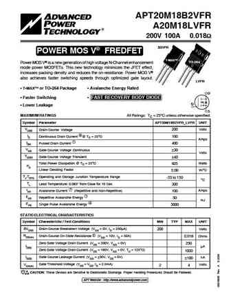
APT20M18B2VFR A20M18LVFR 200V 100A 0.018 B2VFR POWER MOS V FREDFET T-MAX TO-264 Power MOS V is a new generation of high voltage N-Channel enhancement mode power MOSFETs. This new technology minimizes the JFET effect, increases packing density and reduces the on-resistance. Power MOS V also achieves faster switching speeds through optimized gate layout.
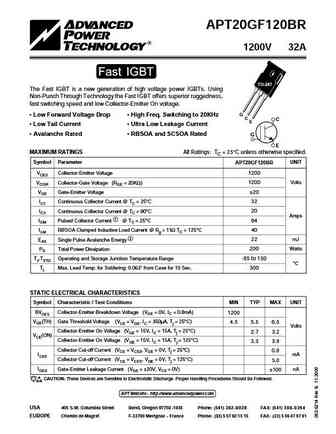
apt20gf120brd.pdf

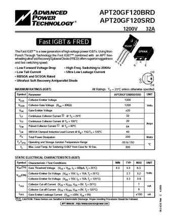
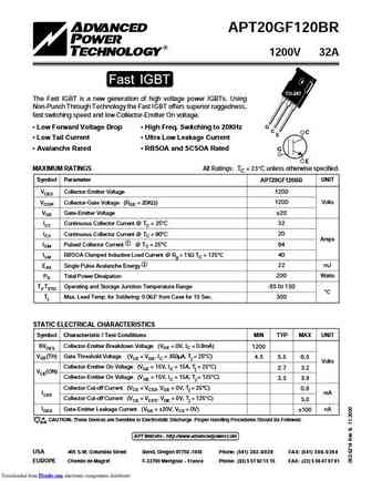
APT20GF120BRD 1200V 32A Fast IGBT & FRED The Fast IGBT is a new generation of high voltage power IGBTs. Using Non- TO-247 Punch Through Technology the Fast IGBT combined with an APT free- wheeling ultraFast Recovery Epitaxial Diode (FRED) offers superior ruggedness and fast switching speed. G Low Forward Voltage Drop High Freq. Switching to 20KHz C C E Low Tail Cur
apt20m36bfllg apt20m36sfllg.pdf
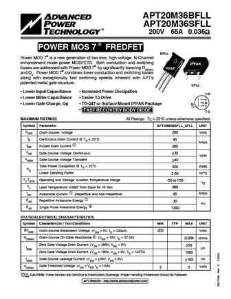
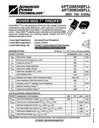
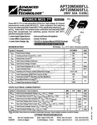
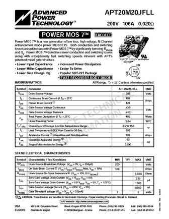
APT20M36BFLL APT20M36SFLL 200V 65A 0.036 R POWER MOS 7 FREDFET BFLL Power MOS 7 is a new generation of low loss, high voltage, N-Channel enhancement mode power MOSFETS. Both conduction and switching D3PAK losses are addressed with Power MOS 7 by significantly lowering RDS(ON) TO-247 and Qg. Power MOS 7 combines lower conduction and switching losses alon
apt20gf120krg.pdf
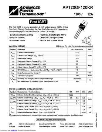
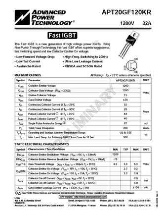
APT20GF120KR APT20GF120KR 1200V 32A Fast IGBT TO-220 The Fast IGBT is a new generation of high voltage power IGBTs. Using Non-Punch Through Technology the Fast IGBT offers superior ruggedness, fast switching speed and low Collector-Emitter On voltage. Low Forward Voltage Drop High Freq. Switching to 20KHz C G C Low Tail Current Ultra Low Leakage Current E Avala
apt20m45svfr.pdf
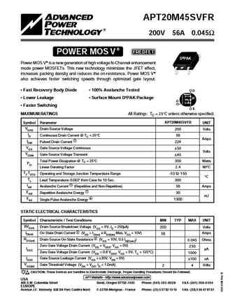
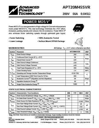
APT20M45SVFR 200V 56A 0.045 POWER MOS V FREDFET D3PAK Power MOS V is a new generation of high voltage N-Channel enhancement mode power MOSFETs. This new technology minimizes the JFET effect, increases packing density and reduces the on-resistance. Power MOS V also achieves faster switching speeds through optimized gate layout. Fast Recovery Body Diode 100% Avalanche Tes
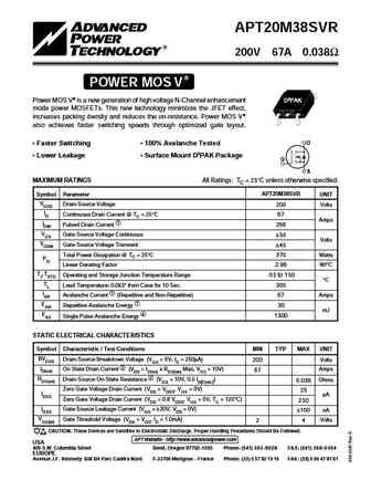
apt20m38bvr.pdf
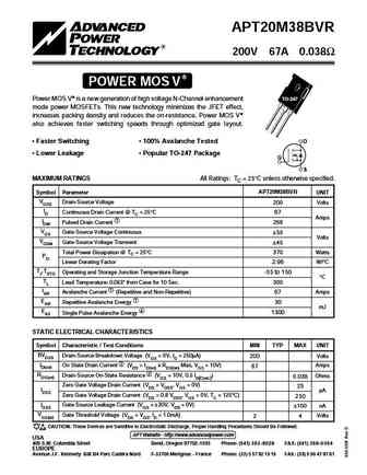
APT20M38BVR 200V 67A 0.038 POWER MOS V Power MOS V is a new generation of high voltage N-Channel enhancement TO-247 mode power MOSFETs. This new technology minimizes the JFET effect, increases packing density and reduces the on-resistance. Power MOS V also achieves faster switching speeds through optimized gate layout. Faster Switching 100% Avalanche Tested D Lower
apt20gf120kr.pdf
APT20GF120KR 1200V 32A Fast IGBT TO-220 The Fast IGBT is a new generation of high voltage power IGBTs. Using Non-Punch Through Technology the Fast IGBT offers superior ruggedness, fast switching speed and low Collector-Emitter On voltage. G C Low Forward Voltage Drop High Freq. Switching to 20KHz E C Low Tail Current Ultra Low Leakage Current Avalanche Rated
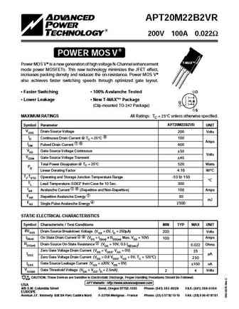
apt20m22lvfr.pdf
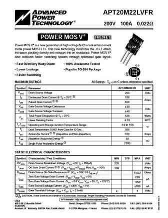
APT20M22LVFR 200V 100A 0.022 POWER MOS V FREDFET Power MOS V is a new generation of high voltage N-Channel enhancement TO-264 mode power MOSFETs. This new technology minimizes the JFET effect, increases packing density and reduces the on-resistance. Power MOS V also achieves faster switching speeds through optimized gate layout. Fast Recovery Body Diode 100% Avalanche T
apt20m18b2vfr.pdf
APT20M18B2VFR APT20M18LVFR 200V 100A 0.018W B2VFR POWER MOS V FREDFET T-MAX Power MOS V is a new generation of high voltage N-Channel enhancement TO-264 mode power MOSFETs. This new technology minimizes the JFET effect, increases packing density and reduces the on-resistance. Power MOS V also achieves faster switching speeds through optimized gate layout. LVFR Identical
apt20m34bll.pdf

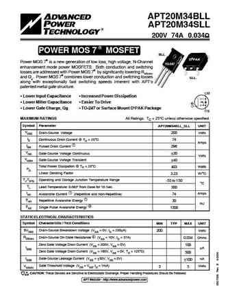
APT20M34BLL APT20M34SLL 200V 74A 0.034W TM BLL POWER MOS 7 Power MOS 7TM is a new generation of low loss, high voltage, N-Channel D3PAK TO-247 enhancement mode power MOSFETS. Both conduction and switching losses are addressed with Power MOS 7TM by significantly lowering RDS(ON) and Qg. Power MOS 7TM combines lower conduction and switching losses along with exceptionally fast switchin
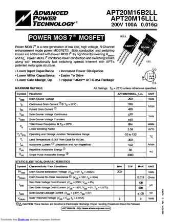
apt20m16b2ll.pdf

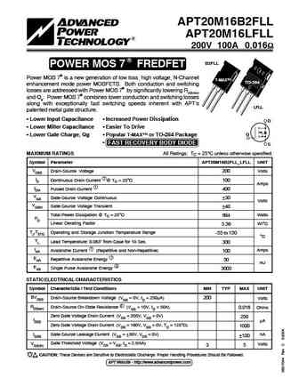
APT20M16B2LL APT20M16LLL 200V 100A 0.016W B2LL TM POWER MOS 7 Power MOS 7TM is a new generation of low loss, high voltage, N-Channel T-MAX TO-264 enhancement mode power MOSFETS. Both conduction and switching losses are addressed with Power MOS 7TM by significantly lowering RDS(ON) and Qg. Power MOS 7TM combines lower conduction and switching losses along with exceptionally fast
apt20m11jll.pdf
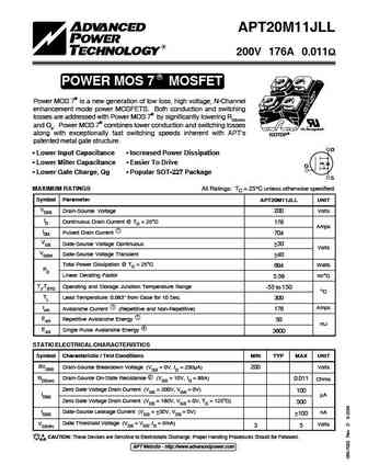
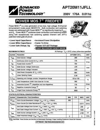
APT20M11JLL 200V 176A 0.011 R POWER MOS 7 MOSFET Power MOS 7 is a new generation of low loss, high voltage, N-Channel enhancement mode power MOSFETS. Both conduction and switching losses are addressed with Power MOS 7 by significantly lowering RDS(ON) and Qg. Power MOS 7 combines lower conduction and switching losses "UL Recognized" along with exceptionall
apt20gt60krg.pdf
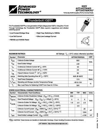
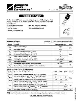
TYPICAL PERFORMANCE CURVES APT20GT60KR(G) 600V APT20GT60KR APT20GT60KRG* *G Denotes RoHS Compliant, Pb Free Terminal Finish. Thunderbolt IGBT TO-220 The Thunderblot IGBT is a new generation of high voltage power IGBTs. Using Non- Punch Through Technology, the Thunderblot IGBT offers superior ruggedness and ultrafast switching speed. Low Forward Voltage Drop High
apt20gf120br.pdf
APT20GF120BR APT20GF120BR 1200V 32A Fast IGBT TO-247 The Fast IGBT is a new generation of high voltage power IGBTs. Using Non-Punch Through Technology the Fast IGBT offers superior ruggedness, fast switching speed and low Collector-Emitter On voltage. G Low Forward Voltage Drop High Freq. Switching to 20KHz C C E Low Tail Current Ultra Low Leakage Current Avala
apt20m40bvr.pdf

APT20M40BVR 200V 59A 0.040 POWER MOS V Power MOS V is a new generation of high voltage N-Channel enhancement TO-247 mode power MOSFETs. This new technology minimizes the JFET effect, increases packing density and reduces the on-resistance. Power MOS V also achieves faster switching speeds through optimized gate layout. Faster Switching 100% Avalanche Tested D Lower
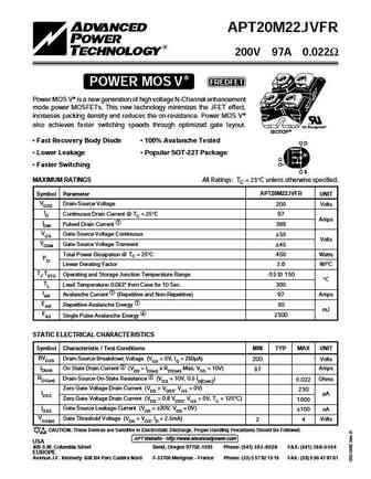
apt20m22jvr.pdf

APT20M22JVR 200V 97A 0.022 POWER MOS V Power MOS V is a new generation of high voltage N-Channel enhancement mode power MOSFETs. This new technology minimizes the JFET effect, increases packing density and reduces the on-resistance. Power MOS V also achieves faster switching speeds through optimized gate layout. "UL Recognized" ISOTOP Faster Switching 100% Avalanche
apt20m11jvfr.pdf
APT20M11JVFR 200V 175A 0.011 POWER MOS V FREDFET Power MOS V is a new generation of high voltage N-Channel enhancement mode power MOSFETs. This new technology minimizes the JFET effect, increases packing density and reduces the on-resistance. Power MOS V also achieves faster switching speeds through optimized gate layout. ISOTOP Fast Recovery Body Diode 100% Avalanche
apt20m16b2llg apt20m16lllg.pdf
APT20M16B2LL APT20M16LLL 200V 100A 0.016 R B2LL POWER MOS 7 MOSFET T-MAX Power MOS 7 is a new generation of low loss, high voltage, N-Channel TO-264 enhancement mode power MOSFETS. Both conduction and switching losses are addressed with Power MOS 7 by significantly lowering RDS(ON) and Qg. Power MOS 7 combines lower conduction and switching losses LL
apt20m38svfrg.pdf
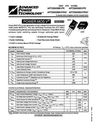
200V 67A 0.038 APT20M38BVFR APT20M38SVFR APT20M38BVFRG* APT20M38SVFRG* *G Denotes RoHS Compliant, Pb Free Terminal Finish. BVFR POWER MOS V FREDFET D3PAK Power MOS V is a new generation of high voltage N-Channel enhancement TO-247 mode power MOSFETs. This new technology minimizes the JFET effect, increases packing density and reduces the on-resistance. Power
apt20m22.pdf

APT20M22JVR 200V 97A 0.022 POWER MOS V Power MOS V is a new generation of high voltage N-Channel enhancement mode power MOSFETs. This new technology minimizes the JFET effect, increases packing density and reduces the on-resistance. Power MOS V also achieves faster switching speeds through optimized gate layout. "UL Recognized" ISOTOP Faster Switching 100% Avalanche
apt20m45bvr.pdf
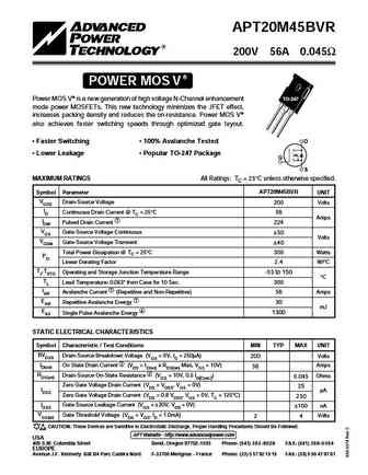
APT20M45BVR 200V 56A 0.045 POWER MOS V Power MOS V is a new generation of high voltage N-Channel enhancement TO-247 mode power MOSFETs. This new technology minimizes the JFET effect, increases packing density and reduces the on-resistance. Power MOS V also achieves faster switching speeds through optimized gate layout. Faster Switching 100% Avalanche Tested D Lower
apt20m42hvr.pdf

APT20M42HVR 200V 50A 0.042W POWER MOS V TO-258 Power MOS V is a new generation of high voltage N-Channel enhancement mode power MOSFETs. This new technology minimizes the JFET effect, increases packing density and reduces the on-resistance. Power MOS V also achieves faster switching speeds through optimized gate layout. D Faster Switching 100% Avalanche Tested Lower
apt20m10jll 1.pdf

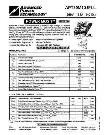
APT20M10JLL 200V 185A 0.010 W TM POWER MOS 7 Power MOS 7TM is a new generation of low loss, high voltage, N-Channel enhancement mode power MOSFETS. Both conduction and switching losses are addressed with Power MOS 7TM by significantly lowering RDS(ON) and Qg. Power MOS 7TM combines lower conduction and switching losses along with exceptionally fast switching speeds inherent with APT's
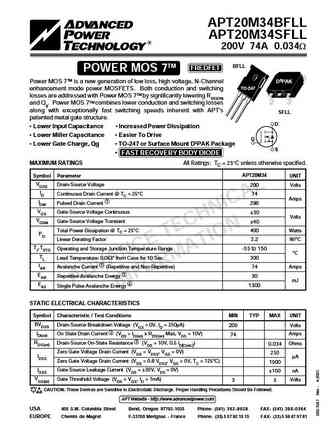
apt20m20b2fll.pdf
APT20M20B2FLL APT20M20LFLL 200V 100A 0.020W TM FREDFET POWER MOS 7 B2FLL Power MOS 7TM is a new generation of low loss, high voltage, N-Channel enhancement mode power MOSFETS. Both conduction and switching T-MAX TO-264 losses are addressed with Power MOS 7TM by significantly lowering RDS(ON) and Qg. Power MOS 7TM combines lower conduction and switching losses along with excepti
apt20m34bfllg apt20m34sfllg.pdf
APT20M34BFLL APT20M34SFLL 200V 74A 0.034 BFLL R POWER MOS 7 FREDFET D3PAK Power MOS 7 is a new generation of low loss, high voltage, N-Channel TO-247 enhancement mode power MOSFETS. Both conduction and switching losses are addressed with Power MOS 7 by significantly lowering RDS(ON) and Qg. Power MOS 7 combines lower conduction and switching losses SFLL
apt20m18b2vr.pdf
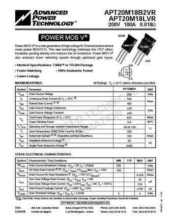
APT20M18B2VR APT20M18LVR 200V 100A 0.018W B2VR POWER MOS V T-MAX Power MOS V is a new generation of high voltage N-Channel enhancement TO-264 mode power MOSFETs. This new technology minimizes the JFET effect, increases packing density and reduces the on-resistance. Power MOS V also achieves faster switching speeds through optimized gate layout. LVR Identical Specificati
apt20gt60brg.pdf
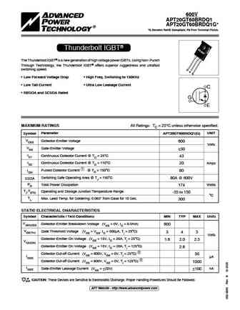
TYPICAL PERFORMANCE CURVES APT20GT60BR(G) 600V APT20GT60BR APT20GT60BRG* *G Denotes RoHS Compliant, Pb Free Terminal Finish. Thunderbolt IGBT The Thunderblot IGBT is a new generation of high voltage power IGBTs. Using Non- Punch Through Technology, the Thunderblot IGBT offers superior ruggedness and ultrafast switching speed. G C E Low Forward Voltage Drop Hig
apt20m45bvfr.pdf

APT20M45BVFR 200V 56A 0.045 POWER MOS V FREDFET Power MOS V is a new generation of high voltage N-Channel enhancement TO-247 mode power MOSFETs. This new technology minimizes the JFET effect, increases packing density and reduces the on-resistance. Power MOS V also achieves faster switching speeds through optimized gate layout. Fast Recovery Body Diode 100% Avalanche Tes
apt20m34bfll.pdf
APT20M34BFLL APT20M34SFLL 200V 74A 0.034W TM BFLL FREDFET POWER MOS 7 Power MOS 7TM is a new generation of low loss, high voltage, N-Channel D3PAK TO-247 enhancement mode power MOSFETS. Both conduction and switching losses are addressed with Power MOS 7TM by significantly lowering RDS(ON) and Qg. Power MOS 7TM combines lower conduction and switching losses along with exceptionally f
apt20m20b2fllg apt20m20lfllg.pdf
APT20M20B2FLL APT20M20LFLL 200V 100A 0.020 R FREDFET POWER MOS 7 FREDFET Power MOS 7 is a new generation of low loss, high voltage, N-Channel T-MAX TO-264 enhancement mode power MOSFETS. Both conduction and switching losses are addressed with Power MOS 7 by significantly lowering RDS(ON) and Qg. Power MOS 7 combines lower conduction and switching loss
apt20m20b2ll.pdf

APT20M20B2LL APT20M20LLL 200V 100A 0.020W B2LL TM POWER MOS 7 Power MOS 7TM is a new generation of low loss, high voltage, N-Channel T-MAX TO-264 enhancement mode power MOSFETS. Both conduction and switching losses are addressed with Power MOS 7TM by significantly lowering RDS(ON) and Qg. Power MOS 7TM combines lower conduction and switching losses along with exceptionally fast
apt20gt60brdq1g.pdf
TYPICAL PERFORMANCE CURVES APT20GT60BRDQ1(G) 600V APT20GT60BRDQ1 APT20GT60BRDQ1G* *G Denotes RoHS Compliant, Pb Free Terminal Finish. Thunderbolt IGBT The Thunderblot IGBT is a new generation of high voltage power IGBTs. Using Non- Punch Through Technology, the Thunderblot IGBT offers superior ruggedness and ultrafast switching speed. G C E Low Forward Voltage Dro
apt20m22b2vfr.pdf

APT20M22B2VFR 200V 100A 0.022 POWER MOS V FREDFET T-MAX Power MOS V is a new generation of high voltage N-Channel enhancement mode power MOSFETs. This new technology minimizes the JFET effect, increases packing density and reduces the on-resistance. Power MOS V also achieves faster switching speeds through optimized gate layout. Fast Recovery Body Diode 100% Avalanch
apt20m26wvr.pdf

APT20M26WVR 200V 65A 0.026 POWER MOS V TO-267 Power MOS V is a new generation of high voltage N-Channel enhancement mode power MOSFETs. This new technology minimizes the JFET effect, increases packing density and reduces the on-resistance. Power MOS V also achieves faster switching speeds through optimized gate layout. Faster Switching 100% Avalanche Tested D Lower
apt20m40hvr.pdf

APT20M40HVR 200V 45A 0.040 POWER MOS V TO-258 Power MOS V is a new generation of high voltage N-Channel enhancement mode power MOSFETs. This new technology minimizes the JFET effect, increases packing density and reduces the on-resistance. Power MOS V also achieves faster switching speeds through optimized gate layout. D Faster Switching 100% Avalanche Tested Lowe
apt20m38bvfr.pdf

APT20M38BVFR 200V 67A 0.038 POWER MOS V FREDFET Power MOS V is a new generation of high voltage N-Channel enhancement TO-247 mode power MOSFETs. This new technology minimizes the JFET effect, increases packing density and reduces the on-resistance. Power MOS V also achieves faster switching speeds through optimized gate layout. Fast Recovery Body Diode 100% Avalanche Tes
apt20m45svr.pdf
APT20M45SVR 200V 56A 0.045 POWER MOS V Power MOS V is a new generation of high voltage N-Channel enhancement D3PAK mode power MOSFETs. This new technology minimizes the JFET effect, increases packing density and reduces the on-resistance. Power MOS V also achieves faster switching speeds through optimized gate layout. Faster Switching 100% Avalanche Tested D Lower L
apt20gf120brdq1g.pdf

TYPICAL PERFORMANCE CURVES APT20GF120B_SRDQ1(G) 1200V APT20GF120BRDQ1 APT20GF120SRDQ1 APT20GF120BRDQ1G* APT20GF120SRDQ1G* *G Denotes RoHS Compliant, Pb Free Terminal Finish. (B) FAST IGBT & FRED D3PAK (S) C The Fast IGBT is a new generation of high voltage power IGBTs. Using Non-Punch through G E technology, the Fast IGBT combined with an APT free wheeling Ultra Fast Recovery
apt20m10jfll.pdf
APT20M10JFLL 200V 185A 0.010W TM FREDFET POWER MOS 7 Power MOS 7TM is a new generation of low loss, high voltage, N-Channel enhancement mode power MOSFETS. Both conduction and switching losses are addressed with Power MOS 7TM by significantly lowering RDS(ON) and Qg. Power MOS 7TM combines lower conduction and switching losses along with exceptionally fast switching speeds inherent wi
apt20gt60br.pdf

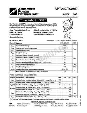
APT20GT60BR APT20GT60BR 600V 40A Thunderbolt IGBT TO-247 The Thunderbolt IGBT is a new generation of high voltage power IGBTs. Using Non-Punch Through Technology the Thunderbolt IGBT offers superior ruggedness and ultrafast switching speed. C Low Forward Voltage Drop High Freq. Switching to 150KHz G C E Low Tail Current Ultra Low Leakage Current G Ava
apt20gf120srdq1g.pdf
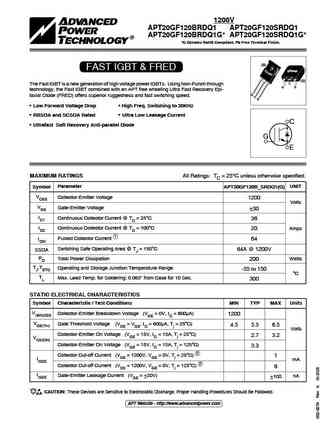
TYPICAL PERFORMANCE CURVES APT20GF120B_SRDQ1(G) 1200V APT20GF120BRDQ1 APT20GF120SRDQ1 APT20GF120BRDQ1G* APT20GF120SRDQ1G* *G Denotes RoHS Compliant, Pb Free Terminal Finish. (B) FAST IGBT & FRED D3PAK (S) C The Fast IGBT is a new generation of high voltage power IGBTs. Using Non-Punch through G E technology, the Fast IGBT combined with an APT free wheeling Ultra Fast Recovery
apt200gn60j.pdf
TYPICAL PERFORMANCE CURVES APT200GN60J 600V APT200GN60J Utilizing the latest Field Stop and Trench Gate technologies, these IGBT's have ultra low VCE(ON) and are ideal for low frequency applications that require absolute minimum conduction loss. Easy paralleling is a result of very tight parameter distribution and a slightly positive VCE(ON) temperature coefficient. A built-in ga
apt20m34bllg apt20m34sllg.pdf
APT20M34BLL APT20M34SLL 200V 74A 0.034 R POWER MOS 7 MOSFET BLL D3PAK Power MOS 7 is a new generation of low loss, high voltage, N-Channel TO-247 enhancement mode power MOSFETS. Both conduction and switching losses are addressed with Power MOS 7 by significantly lowering RDS(ON) and Qg. Power MOS 7 combines lower conduction and switching losses SLL alo
apt20m13pvr.pdf
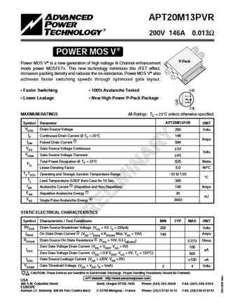
APT20M13PVR 200V 146A 0.013 POWER MOS V P-Pack Power MOS V is a new generation of high voltage N-Channel enhancement mode power MOSFETs. This new technology minimizes the JFET effect, increases packing density and reduces the on-resistance. Power MOS V also achieves faster switching speeds through optimized gate layout. Faster Switching 100% Avalanche Tested D Lowe
apt20m11jvr.pdf

APT20M11JVR 200V 175A 0.011 POWER MOS V Power MOS V is a new generation of high voltage N-Channel enhancement mode power MOSFETs. This new technology minimizes the JFET effect, increases packing density and reduces the on-resistance. Power MOS V also achieves faster switching speeds through optimized gate layout. "UL Recognized" ISOTOP Faster Switching 100% Avalanche
apt20gf120srd.pdf
APT20GF120BRD APT20GF120SRD 1200V 32A Fast IGBT & FRED TO-247 The Fast IGBT is a new generation of high voltage power IGBTs. Using Non- D3PAK Punch Through Technology the Fast IGBT combined with an APT free- wheeling ultraFast Recovery Epitaxial Diode (FRED) offers superior ruggedness G C and fast switching speed. C E G E Low Forward Voltage Drop High Freq. Switching
apt20m10jll.pdf

APT20M10JLL 200V 185A 0.010W TM POWER MOS 7 Power MOS 7TM is a new generation of low loss, high voltage, N-Channel enhancement mode power MOSFETS. Both conduction and switching losses are addressed with Power MOS 7TM by significantly lowering RDS(ON) and Qg. Power MOS 7TM combines lower conduction and switching losses along with exceptionally fast switching speeds inherent with APT's
apt20m16b2fllg apt20m16lfllg.pdf
APT20M16B2FLL APT20M16LFLL 200V 100A 0.016 R B2FLL POWER MOS 7 FREDFET Power MOS 7 is a new generation of low loss, high voltage, N-Channel T-MAX TO-264 enhancement mode power MOSFETS. Both conduction and switching losses are addressed with Power MOS 7 by significantly lowering RDS(ON) and Qg. Power MOS 7 combines lower conduction and switching losses
apt20m36bfll.pdf
APT20M36BFLL APT20M36SFLL 200V 65A 0.036W TM BFLL FREDFET POWER MOS 7 Power MOS 7TM is a new generation of low loss, high voltage, N-Channel D3PAK TO-247 enhancement mode power MOSFETS. Both conduction and switching losses are addressed with Power MOS 7TM by significantly lowering RDS(ON) and Qg. Power MOS 7TM combines lower conduction and switching losses along with exceptionally f
apt200gn60jdq4.pdf
TYPICAL PERFORMANCE CURVES APT200GN60JDQ4 600V APT200GN60JDQ4 Utilizing the latest Field Stop and Trench Gate technologies, these IGBT's have ultra low VCE(ON) and are ideal for low frequency applications that require absolute minimum conduction loss. Easy paralleling is a result of very tight parameter distribution and a slightly positive VCE(ON) temperature coefficient. A built
apt20m19jvr.pdf
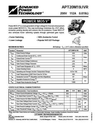
APT20M19JVR 200V 112A 0.019 POWER MOS V Power MOS V is a new generation of high voltage N-Channel enhancement mode power MOSFETs. This new technology minimizes the JFET effect, increases packing density and reduces the on-resistance. Power MOS V also achieves faster switching speeds through optimized gate layout. "UL Recognized" ISOTOP Faster Switching 100% Avalanche
apt20gf120brg.pdf
APT20GF120BR APT20GF120BR 1200V 32A Fast IGBT TO-247 The Fast IGBT is a new generation of high voltage power IGBTs. Using Non-Punch Through Technology the Fast IGBT offers superior ruggedness, fast switching speed and low Collector-Emitter On voltage. G Low Forward Voltage Drop High Freq. Switching to 20KHz C C E Low Tail Current Ultra Low Leakage Current Avala
apt20m20b2llg apt20m20lllg.pdf
APT20M20B2LL APT20M20LLL 200V 100A 0.020 R POWER MOS 7 MOSFET T-MAX Power MOS 7 is a new generation of low loss, high voltage, N-Channel TO-264 enhancement mode power MOSFETS. Both conduction and switching losses are addressed with Power MOS 7 by significantly lowering RDS(ON) and Qg. Power MOS 7 combines lower conduction and switching losses along wi
apt20m11jfll.pdf
APT20M11JFLL 200V 176A 0.011 R POWER MOS 7 FREDFET Power MOS 7 is a new generation of low loss, high voltage, N-Channel enhancement mode power MOSFETS. Both conduction and switching losses are addressed with Power MOS 7 by significantly lowering RDS(ON) and Qg. Power MOS 7 combines lower conduction and switching losses along with exceptionally fast switchin
apt20m20jll.pdf
APT20M20JLL 200V 106A 0.020 W TM POWER MOS 7 Power MOS 7TM is a new generation of low loss, high voltage, N-Channel enhancement mode power MOSFETS. Both conduction and switching losses are addressed with Power MOS 7TM by significantly lowering RDS(ON) and Qg. Power MOS 7TM combines lower conduction and switching losses along with exceptionally fast switching speeds inherent with APT's
apt20m38svr.pdf
APT20M38SVR 200V 67A 0.038 POWER MOS V Power MOS V is a new generation of high voltage N-Channel enhancement D3PAK mode power MOSFETs. This new technology minimizes the JFET effect, increases packing density and reduces the on-resistance. Power MOS V also achieves faster switching speeds through optimized gate layout. D Faster Switching 100% Avalanche Tested Lower
apt20m16b2fll.pdf

APT20M16B2FLL APT20M16LFLL 200V 100A 0.016W TM FREDFET POWER MOS 7 B2FLL Power MOS 7TM is a new generation of low loss, high voltage, N-Channel enhancement mode power MOSFETS. Both conduction and switching T-MAX TO-264 losses are addressed with Power MOS 7TM by significantly lowering RDS(ON) and Qg. Power MOS 7TM combines lower conduction and switching losses along with excepti
apt20m22b2vr.pdf
APT20M22B2VR 200V 100A 0.022 POWER MOS V T-MAX Power MOS V is a new generation of high voltage N-Channel enhancement mode power MOSFETs. This new technology minimizes the JFET effect, increases packing density and reduces the on-resistance. Power MOS V also achieves faster switching speeds through optimized gate layout. Faster Switching 100% Avalanche Tested D L
apt20gt60kr.pdf
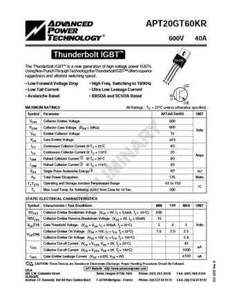
APT20GT60KR 600V 40A Thunderbolt IGBT TO-220 The Thunderbolt IGBT is a new generation of high voltage power IGBTs. Using Non-Punch Through Technology the Thunderbolt IGBT offers superior ruggedness and ultrafast switching speed. G C Low Forward Voltage Drop High Freq. Switching to 150KHz E C Low Tail Current Ultra Low Leakage Current Avalanche Rated
apt20m22lvr.pdf
APT20M22LVR 200V 100A 0.022 POWER MOS V Power MOS V is a new generation of high voltage N-Channel enhancement TO-264 mode power MOSFETs. This new technology minimizes the JFET effect, increases packing density and reduces the on-resistance. Power MOS V also achieves faster switching speeds through optimized gate layout.. Faster Switching 100% Avalanche Tested D Low
apt20m20jfll.pdf
APT20M20JFLL 200V 106A 0.020W TM FREDFET POWER MOS 7 Power MOS 7TM is a new generation of low loss, high voltage, N-Channel enhancement mode power MOSFETS. Both conduction and switching losses are addressed with Power MOS 7TM by significantly lowering RDS(ON) and Qg. Power MOS 7TM combines lower conduction and switching losses along with exceptionally fast switching speeds inherent wi
apt20gt60cr.pdf
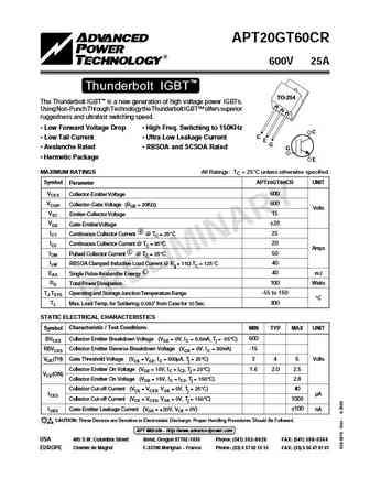
APT20GT60CR 600V 25A Thunderbolt IGBT TO-254 TO-254 TO-254 The Thunderbolt IGBT is a new generation of high voltage power IGBTs. Using Non-Punch Through Technology the Thunderbolt IGBT offers superior ruggedness and ultrafast switching speed. Low Forward Voltage Drop High Freq. Switching to 150KHz C C Low Tail Current Ultra Low Leakage Current E G Ava
apt20m36bll.pdf

APT20M36BLL APT20M36SLL 200V 65A 0.036W TM BLL POWER MOS 7 Power MOS 7TM is a new generation of low loss, high voltage, N-Channel D3PAK TO-247 enhancement mode power MOSFETS. Both conduction and switching losses are addressed with Power MOS 7TM by significantly lowering RDS(ON) and Qg. Power MOS 7TM combines lower conduction and switching losses along with exceptionally fast switchin
apt20m120jcu3.pdf
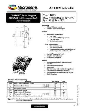
APT20M120JCU3 VDSS = 1200V ISOTOP Buck chopper RDSon = 560m typ @ Tj = 25 C MOSFET + SiC chopper diode ID = 20A @ Tc = 25 C Power module Application D AC and DC motor control Switched Mode Power Supplies Features Power MOS 8 MOSFET G - Low RDSon S - Low input and Miller capacitance - Low gate charge - Avalanche energy rated SiC Schott
apt200gn60b2g.pdf
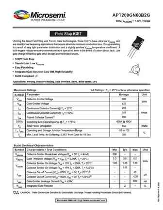
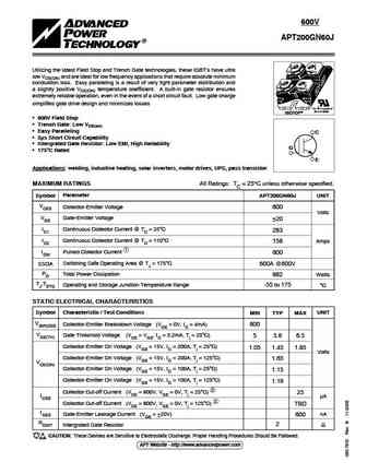
APT200GN60B2G 600V, VCE(ON) = 1.45V Typical Field Stop IGBT Utilizing the latest Field Stop and Trench Gate technologies, these IGBT s have ultra low VCE(ON) and are ideal for low frequency applications that require absolute minimum conduction loss. Easy paralleling is a result of very tight parameter distribution and a slightly positive VCE(ON) temperature coefficient. A built-in g
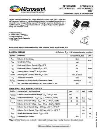
apt20gn60kg.pdf
TYPICAL PERFORMANCE CURVES APT20GN60K(G) 600V APT20GN60K APT20GN60KG* *G Denotes RoHS Compliant, Pb Free Terminal Finish. Utilizing the latest Field Stop and Trench Gate technologies, these IGBT's have ultra low VCE(ON) and are ideal for low frequency applications that require absolute minimum conduction loss. Easy paralleling is a result of very tight parameter distribution and a
apt200gt60jr.pdf
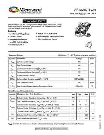
APT200GT60JR 600V, 200A, VCE(ON) = 2.1V Typical Thunderbolt IGBT The Thunderbolt IGBT is a new generation of high voltage power IGBTs. Using Non-Punch-Through Technology, the Thunderbolt IGBT offers superior rugged- ness and ultrafast switching speed. Features RBSOA and SCSOA Rated Low Forward Voltage Drop "UL Recognized" High Frequency Switching to 50KHz Lo
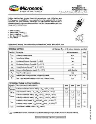
apt20gn60bg apt20gn60sg.pdf
TYPICAL PERFORMANCE CURVES APT20GN60B_S(G) APT20GN60B APT20GN60S APT20GN60B(G) APT20GN60S(G) 600V *G Denotes RoHS Compliant, Pb Free Terminal Finish. Utilizing the latest Field Stop and Trench Gate technologies, these IGBT's have ultra (B) low VCE(ON) and are ideal for low frequency applications that require absolute minimum conduction loss. Easy paralleling is a result of very
apt200gt60jrdl.pdf
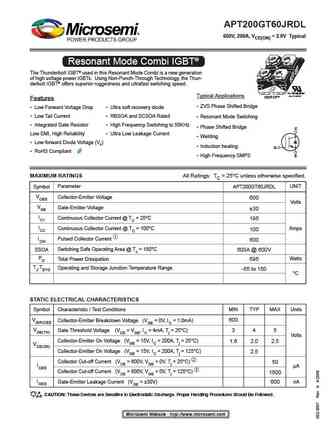
TYPICAL PERFORMANCE CURVES APT200GT60JRDL APT200GT60JRDL 600V, 200A, VCE(ON) = 2.0V Typical Resonant Mode Combi IGBT The Thunderbolt IGBT used in this Resonant Mode Combi is a new generation of high voltage power IGBTs. Using Non-Punch-Through Technology, the Thun- derbolt IGBT offers superior ruggedness and ultrafast switching speed. "UL Recognized" Typical Applications ISOTOP
apt20f50b apt20f50s.pdf
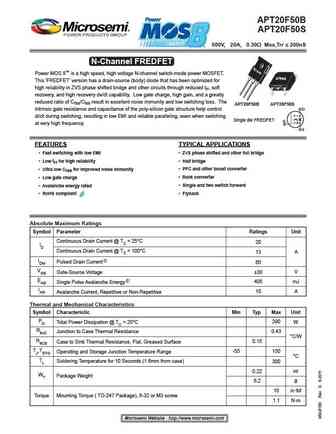
APT20F50B APT20F50S 500V, 20A, 0.30 Max,Trr 200nS N-Channel FREDFET Power MOS 8 is a high speed, high voltage N-channel switch-mode power MOSFET. D3PAK This 'FREDFET' version has a drain-source (body) diode that has been optimized for high reliability in ZVS phase shifted bridge and other circuits through reduced trr, soft recovery, and high recovery dv/dt capability. Low
apt20m120jcu2.pdf
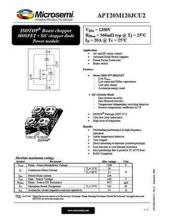
APT20M120JCU2 VDSS = 1200V ISOTOP Boost chopper RDSon = 560m typ @ Tj = 25 C MOSFET + SiC chopper diode ID = 20A @ Tc = 25 C Power module Application K AC and DC motor control Switched Mode Power Supplies Power Factor Correction D Brake switch Features Power MOS 8 MOSFET G - Low RDSon - Low input and Miller capacitance - Low gat
apt20m38bvr.pdf

isc N-Channel MOSFET Transistor APT20M38BVR FEATURES Drain Current I =67A@ T =25 D C Drain Source Voltage- V =200V(Min) DSS Static Drain-Source On-Resistance R =0.038 (Max) DS(on) 100% avalanche tested Minimum Lot-to-Lot variations for robust device performance and reliable operation DESCRIPTION Designed for use in switch mode power supplies and general pur
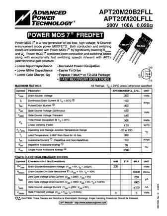
apt20m22lvfr.pdf
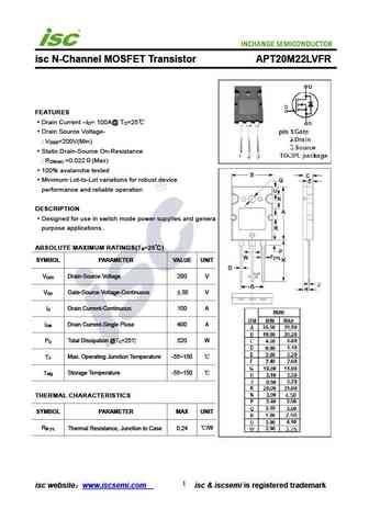
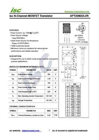
isc N-Channel MOSFET Transistor APT20M22LVFR FEATURES Drain Current I = 100A@ T =25 D C Drain Source Voltage- V =200V(Min) DSS Static Drain-Source On-Resistance R =0.022 (Max) DS(on) 100% avalanche tested Minimum Lot-to-Lot variations for robust device performance and reliable operation DESCRIPTION Designed for use in switch mode power supplies and general
apt20m16lfll.pdf
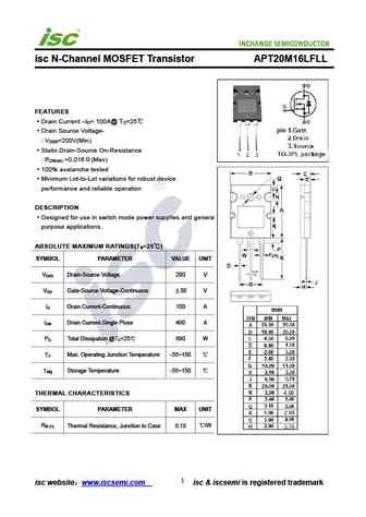
isc N-Channel MOSFET Transistor APT20M16LFLL FEATURES Drain Current I = 100A@ T =25 D C Drain Source Voltage- V =200V(Min) DSS Static Drain-Source On-Resistance R =0.016 (Max) DS(on) 100% avalanche tested Minimum Lot-to-Lot variations for robust device performance and reliable operation DESCRIPTION Designed for use in switch mode power supplies and general
apt20m18b2vfr.pdf

isc N-Channel MOSFET Transistor APT20M18B2VFR FEATURES Drain Current I = 100A@ T =25 D C Drain Source Voltage- V =200V(Min) DSS Static Drain-Source On-Resistance R =0.018 (Max) DS(on) 100% avalanche tested Minimum Lot-to-Lot variations for robust device performance and reliable operation DESCRIPTION Designed for use in switch mode power supplies and general
apt20m34bll.pdf

isc N-Channel MOSFET Transistor APT20M34BLL FEATURES Drain Current I =74A@ T =25 D C Drain Source Voltage- V =200V(Min) DSS Static Drain-Source On-Resistance R =0.034 (Max) DS(on) 100% avalanche tested Minimum Lot-to-Lot variations for robust device performance and reliable operation DESCRIPTION Designed for use in switch mode power supplies and general pur
apt20m16b2ll.pdf

isc N-Channel MOSFET Transistor APT20M16B2LL FEATURES Drain Current I = 100A@ T =25 D C Drain Source Voltage- V =200V(Min) DSS Static Drain-Source On-Resistance R =0.016 (Max) DS(on) 100% avalanche tested Minimum Lot-to-Lot variations for robust device performance and reliable operation DESCRIPTION Designed for use in switch mode power supplies and general
apt20m18lvfr.pdf

isc N-Channel MOSFET Transistor APT20M18LVFR FEATURES Drain Current I = 100A@ T =25 D C Drain Source Voltage- V =200V(Min) DSS Static Drain-Source On-Resistance R =0.018 (Max) DS(on) 100% avalanche tested Minimum Lot-to-Lot variations for robust device performance and reliable operation DESCRIPTION Designed for use in switch mode power supplies and general
apt20m20lfll.pdf
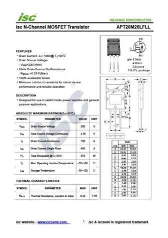
isc N-Channel MOSFET Transistor APT20M20LFLL FEATURES Drain Current I = 100A@ T =25 D C Drain Source Voltage- V =200V(Min) DSS Static Drain-Source On-Resistance R =0.02 (Max) DS(on) 100% avalanche tested Minimum Lot-to-Lot variations for robust device performance and reliable operation DESCRIPTION Designed for use in switch mode power supplies and general p
apt20m18lvr.pdf

isc N-Channel MOSFET Transistor APT20M18LVR FEATURES Drain Current I = 100A@ T =25 D C Drain Source Voltage- V =200V(Min) DSS Static Drain-Source On-Resistance R =0.018 (Max) DS(on) 100% avalanche tested Minimum Lot-to-Lot variations for robust device performance and reliable operation DESCRIPTION Designed for use in switch mode power supplies and general p
apt20m45bvr.pdf

isc N-Channel MOSFET Transistor APT20M45BVR FEATURES Drain Current I =56A@ T =25 D C Drain Source Voltage- V =200V(Min) DSS Static Drain-Source On-Resistance R =0.045 (Max) DS(on) 100% avalanche tested Minimum Lot-to-Lot variations for robust device performance and reliable operation DESCRIPTION Designed for use in switch mode power supplies and general pur
apt20m20b2fll.pdf

isc N-Channel MOSFET Transistor APT20M20B2FLL FEATURES Drain Current I = 100A@ T =25 D C Drain Source Voltage- V =200V(Min) DSS Static Drain-Source On-Resistance R =0.02 (Max) DS(on) 100% avalanche tested Minimum Lot-to-Lot variations for robust device performance and reliable operation DESCRIPTION Designed for use in switch mode power supplies and general
apt20m18b2vr.pdf

isc N-Channel MOSFET Transistor APT20M18B2VR FEATURES Drain Current I = 100A@ T =25 D C Drain Source Voltage- V =200V(Min) DSS Static Drain-Source On-Resistance R =0.018 (Max) DS(on) 100% avalanche tested Minimum Lot-to-Lot variations for robust device performance and reliable operation DESCRIPTION Designed for use in switch mode power supplies and general
apt20m45bvfr.pdf

isc N-Channel MOSFET Transistor APT20M45BVFR FEATURES Drain Current I = 56A@ T =25 D C Drain Source Voltage- V =200V(Min) DSS Static Drain-Source On-Resistance R =0.045 (Max) DS(on) 100% avalanche tested Minimum Lot-to-Lot variations for robust device performance and reliable operation DESCRIPTION Designed for use in switch mode power supplies and general p
apt20m34bfll.pdf
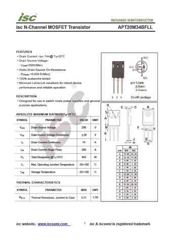
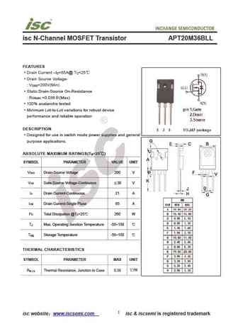
isc N-Channel MOSFET Transistor APT20M34BFLL FEATURES Drain Current I = 74A@ T =25 D C Drain Source Voltage- V =200V(Min) DSS Static Drain-Source On-Resistance R =0.034 (Max) DS(on) 100% avalanche tested Minimum Lot-to-Lot variations for robust device performance and reliable operation DESCRIPTION Designed for use in switch mode power supplies and general p
apt20m20b2ll.pdf
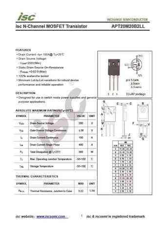
isc N-Channel MOSFET Transistor APT20M20B2LL FEATURES Drain Current I = 100A@ T =25 D C Drain Source Voltage- V =200V(Min) DSS Static Drain-Source On-Resistance R =0.02 (Max) DS(on) 100% avalanche tested Minimum Lot-to-Lot variations for robust device performance and reliable operation DESCRIPTION Designed for use in switch mode power supplies and general p
apt20m36bfll.pdf
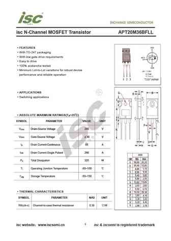
isc N-Channel MOSFET Transistor APT20M36BFLL FEATURES With TO-247 packaging With low gate drive requirements Easy to drive 100% avalanche tested Minimum Lot-to-Lot variations for robust device performance and reliable operation APPLICATIONS Switching applications ABSOLUTE MAXIMUM RATINGS(T =25 ) a SYMBOL PARAMETER VALUE UNIT V Drain-Source Voltage 200 V DSS V
apt20m16b2fll.pdf

isc N-Channel MOSFET Transistor APT20M16B2FLL FEATURES Drain Current I = 100A@ T =25 D C Drain Source Voltage- V =200V(Min) DSS Static Drain-Source On-Resistance R =0.016 (Max) DS(on) 100% avalanche tested Minimum Lot-to-Lot variations for robust device performance and reliable operation DESCRIPTION Designed for use in switch mode power supplies and general
apt20m22lvr.pdf
isc N-Channel MOSFET Transistor APT20M22LVR FEATURES Drain Current I = 100A@ T =25 D C Drain Source Voltage- V =200V(Min) DSS Static Drain-Source On-Resistance R =0.022 (Max) DS(on) 100% avalanche tested Minimum Lot-to-Lot variations for robust device performance and reliable operation DESCRIPTION Designed for use in switch mode power supplies and general p
apt20m36bll.pdf
isc N-Channel MOSFET Transistor APT20M36BLL FEATURES Drain Current I =65A@ T =25 D C Drain Source Voltage- V =200V(Min) DSS Static Drain-Source On-Resistance R =0.036 (Max) DS(on) 100% avalanche tested Minimum Lot-to-Lot variations for robust device performance and reliable operation DESCRIPTION Designed for use in switch mode power supplies and general pur
Другие IGBT... APT20M20B2LL, APT20M20JFLL, APT20M20JLL, APT20M34BFLL, APT20M34BLL, APT20M36BFLL, APT20M36BLL, 2SK310, IRF530, APT30M17JLL, APT30M30B2LL, APT30M30JLL, APT30M36B2LL, APT30M36JLL, APT30M40B2VR, APT30M61BLL, APT30M75BLL
🌐 : EN ES РУ

Список транзисторов
Обновления
MOSFET: FTF30P35D | FTF25N35DHVT | FTF15N35D | FTE15C35G | FTP02P15G | FTE02P15G | AKF30N5P0SX | AKF30N10S | AKF20P45D | CM4407 | CM3407 | CM3400 | SVF11N65F | SVF11N65T | FKBB3105 | EHBA036R1
Popular searches
mje15031 | irfp150n | mj15025 | mp1620 | kta1381 | bf494 | 2sc1885 | skd502t