2SK2459N. Аналоги и основные параметры
Наименование производителя: 2SK2459N
Тип транзистора: MOSFET
Полярность: N
Предельные значения
Pd ⓘ - Максимальная рассеиваемая мощность: 30 W
|Vds|ⓘ - Максимально допустимое напряжение сток-исток: 200 V
|Vgs|ⓘ - Максимально допустимое напряжение затвор-исток: 30 V
|Id| ⓘ - Максимально допустимый постоянный ток стока: 5 A
Tj ⓘ - Максимальная температура канала: 150 °C
Электрические характеристики
tr ⓘ - Время нарастания: 15 ns
Cossⓘ - Выходная емкость: 150 pf
RDSonⓘ - Сопротивление сток-исток открытого транзистора: 0.65 Ohm
Тип корпуса: TO220FN
Аналог (замена) для 2SK2459N
- подборⓘ MOSFET транзистора по параметрам
2SK2459N даташит
2sk2459n.pdf
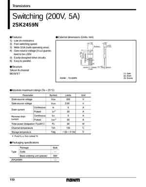
Transistors Switching (200V, 5A) 2SK2459N FFeatures FExternal dimensions (Units mm) 1) Low on-resistance. 2) Fast switching speed. 3) Wide SOA (safe operating area). 4) Gate-source voltage (VGSS) guaran- teed to be 30V. 5) Easily designed drive circuits. 6) Easy to parallel. FStructure Silicon N-channel MOSFET FAbsolute maximum ratings (Ta = 25_C) FPackaging specifications 1
2sk2471-01.pdf
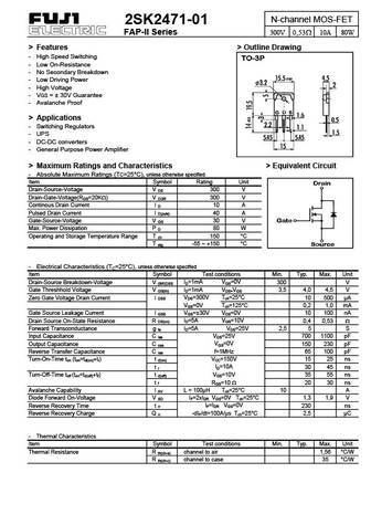
N-channel MOS-FET 2SK2471-01 FAP-II Series 300V 0,53 10A 80W > Features > Outline Drawing - High Speed Switching - Low On-Resistance - No Secondary Breakdown - Low Driving Power - High Voltage - VGS = 30V Guarantee - Avalanche Proof > Applications - Switching Regulators - UPS - DC-DC converters - General Purpose Power Amplifier > Maximum Ratings and Characteristics > Equiv
2sk2499 2sk2499-z.pdf
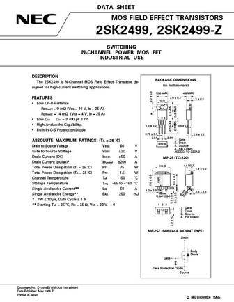
DATA SHEET MOS FIELD EFFECT TRANSISTORS 2SK2499, 2SK2499-Z SWITCHING N-CHANNEL POWER MOS FET INDUSTRIAL USE DESCRIPTION PACKAGE DIMENSIONS The 2SK2499 is N-Channel MOS Field Effect Transistor de- (in millimeters) signed for high current switching applications. 10.6 MAX. 4.8 MAX. 3.6 0.2 FEATURES 1.3 0.2 10.0 Low On-Resistance RDS(on)1 = 9 m (VGS = 10 V, ID = 25 A)
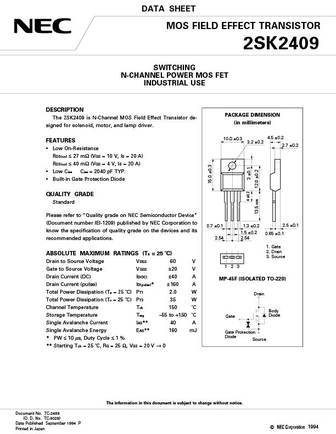
2sk2479.pdf
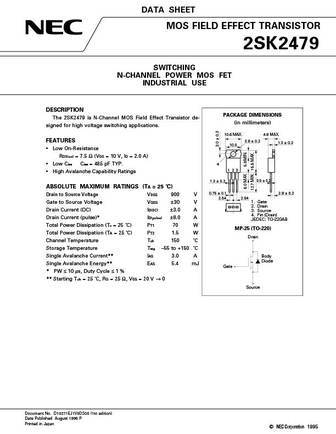
DATA SHEET MOS FIELD EFFECT TRANSISTOR 2SK2479 SWITCHING N-CHANNEL POWER MOS FET INDUSTRIAL USE DESCRIPTION PACKAGE DIMENSIONS The 2SK2479 is N-Channel MOS Field Effect Transistor de- (in millimeters) signed for high voltage switching applications. 10.6 MAX. 4.8 MAX. FEATURES 3.6 0.2 1.3 0.2 10.0 Low On-Resistance RDS(on) = 7.5 (VGS = 10 V, ID = 2.0 A) Low Cis
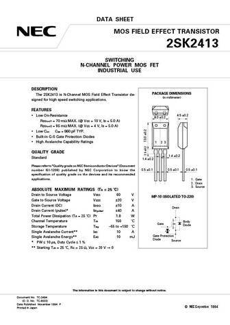
2sk2412.pdf
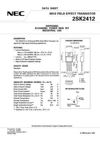
DATA SHEET MOS FIELD EFFECT TRANSISTOR 2SK2412 SWITCHING N-CHANNEL POWER MOS FET INDUSTRIAL USE DESCRIPTION PACKAGE DIMENSIONS The 2SK2412 is N-Channel MOS Field Effect Transistor de- (in millimeters) signed for high speed switching applications. 10.0 0.3 4.5 0.2 3.2 0.2 FEATURES 2.7 0.2 Low On-Resistance RDS(on)1 = 70 m MAX. (@ VGS = 10 V, ID = 10 A) RDS(on)2 =
2sk2419.pdf
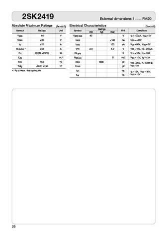
2SK2419 External dimensions 1 ...... FM20 Absolute Maximum Ratings Electrical Characteristics (Ta = 25 C) (Ta = 25 C) Ratings Symbol Ratings Unit Symbol Unit Conditions min typ max V 60 V V 60 V I = 100 A, V = 0V DSS (BR) DSS D GS V 20 V I 100 nA V = 20V GSS GSS GS I 22 A I 100 A V = 60V, V = 0V D DSS DS GS I 88 A V 2.0 4.0 V V = 10V, I = 250 A D (pulse) TH DS D
2sk2477.pdf

DATA SHEET MOS FIELD EFFECT TRANSISTOR 2SK2477 SWITCHING N-CHANNEL POWER MOS FET INDUSTRIAL USE DESCRIPTION PACKAGE DIMENSIONS The 2SK2477 is N-Channel MOS Field Effect Transistor designed (in millimeter) for high voltage switching applications. FEATURES 4.7 MAX. 15.7 MAX. 3.2 0.2 1.5 Low On-Resistance RDS (on) = 1.0 (VGS = 10 V, ID = 5.0 A) 4 Low Ciss Ciss = 2 950
2sk2469-01mr.pdf
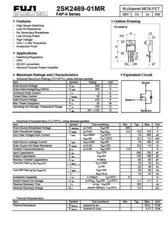
N-channel MOS-FET 2SK2469-01MR FAP-II Series 300V 1 5A 30W > Features > Outline Drawing - High Speed Switching - Low On-Resistance - No Secondary Breakdown - Low Driving Power - High Voltage - VGS = 30V Guarantee - Avalanche Proof > Applications - Switching Regulators - UPS - DC-DC converters - General Purpose Power Amplifier > Maximum Ratings and Characteristics > Equival
2sk2476.pdf

DATA SHEET MOS FIELD EFFECT TRANSISTOR 2SK2476 SWITCHING N-CHANNEL POWER MOS FET INDUSTRIAL USE DESCRIPTION PACKAGE DIMENSIONS The 2SK2476 is N-Channel MOS Field Effect Transistor designed (in millimeter) for high voltage switching applications. FEATURES 10.0 0.3 4.5 0.2 3.2 0.2 Low On-Resistance 2.7 0.2 RDS (on) = 5.0 (VGS = 10 V, ID = 2.0 A) Low Ciss Ciss = 59
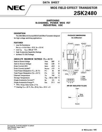
2sk2480.pdf

DATA SHEET MOS FIELD EFFECT TRANSISTOR 2SK2480 SWITCHING N-CHANNEL POWER MOS FET INDUSTRIAL USE DESCRIPTION PACKAGE DIMENSIONS The 2SK2480 is N-Channel MOS Field Effect Transistor designed (in millimeter) for high voltage switching applications. FEATURES 10.0 0.3 4.5 0.2 3.2 0.2 Low On-Resistance 2.7 0.2 RDS (on) = 4.0 (VGS = 10 V, ID = 2.0 A) Low Ciss Ciss = 90
2sk2461.pdf
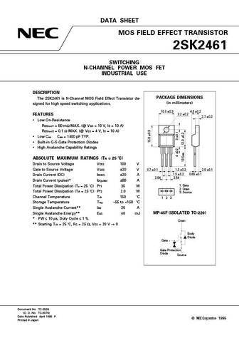
DATA SHEET MOS FIELD EFFECT TRANSISTOR 2SK2461 SWITCHING N-CHANNEL POWER MOS FET INDUSTRIAL USE DESCRIPTION PACKAGE DIMENSIONS The 2SK2461 is N-Channel MOS Field Effect Transistor de- (in millimeters) signed for high speed switching applications. 10.0 0.3 4.5 0.2 3.2 0.2 FEATURES 2.7 0.2 Low On-Resistance RDS(on)1 = 80 m MAX. (@ VGS = 10 V, ID = 10 A) RDS(on)2 =
2sk2410.pdf
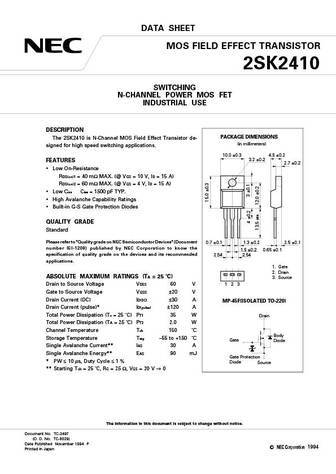
DATA SHEET MOS FIELD EFFECT TRANSISTOR 2SK2410 SWITCHING N-CHANNEL POWER MOS FET INDUSTRIAL USE DESCRIPTION PACKAGE DIMENSIONS The 2SK2410 is N-Channel MOS Field Effect Transistor de- (in millimeters) signed for high speed switching applications. 10.0 0.3 4.5 0.2 3.2 0.2 FEATURES 2.7 0.2 Low On-Resistance RDS(on)1 = 40 m MAX. (@ VGS = 10 V, ID = 15 A) RDS(on)2 =
2sk2498.pdf
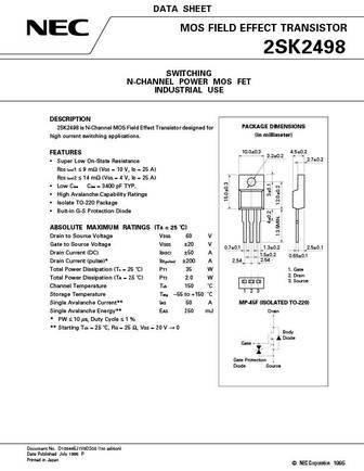
DATA SHEET MOS FIELD EFFECT TRANSISTOR 2SK2498 SWITCHING N-CHANNEL POWER MOS FET INDUSTRIAL USE DESCRIPTION PACKAGE DIMENSIONS 2SK2498 is N-Channel MOS Field Effect Transistor designed for (in millimeter) high current switching applications. 10.0 0.3 4.5 0.2 FEATURES 3.2 0.2 2.7 0.2 Super Low On-State Resistance RDS (on)1 9 m (VGS = 10 V, ID = 25 A) RDS (on)2
2sk2494-01.pdf
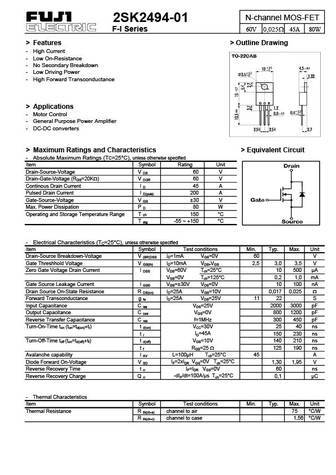
N-channel MOS-FET 2SK2494-01 F-I Series 60V 0,025 45A 80W > Features > Outline Drawing - High Current - Low On-Resistance - No Secondary Breakdown - Low Driving Power - High Forward Transconductance > Applications - Motor Control - General Purpose Power Amplifier - DC-DC converters > Maximum Ratings and Characteristics > Equivalent Circuit - Absolute Maximum Ratings (TC=25 C),
2sk2470-01mr.pdf
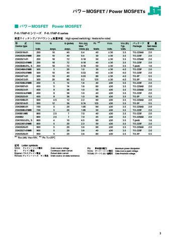
MOSFET / P wer MOSFETs MOSFET P wer MOSFET F II F II F II F II Hi h p d witchin Av l nch r t d 2 VDSS ID ID (pulse) RDS (on) PD VGSS VGS (th) 1 Device type Max. Typ. Package Net mass Volts Amps. Amps. Ohms ( ) Watts V
2sk2478.pdf

DATA SHEET MOS FIELD EFFECT TRANSISTOR 2SK2478 SWITCHING N-CHANNEL POWER MOS FET INDUSTRIAL USE DESCRIPTION PACKAGE DIMENSIONS The 2SK2478 is N-Channel MOS Field Effect Transistor designed (in millimeter) for high voltage switching applications. FEATURES 10.0 0.3 4.5 0.2 3.2 0.2 Low On-Resistance 2.7 0.2 RDS (on) = 7.5 (VGS = 10 V, ID = 1.0 A) Low Ciss Ciss = 48
2sk2473-01.pdf
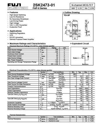
N-channel MOS-FET 2SK2473-01 FAP-II Series 300V 0,2 20A 125W > Features > Outline Drawing - High Speed Switching - Low On-Resistance - No Secondary Breakdown - Low Driving Power - High Voltage - VGS = 30V Guarantee - Avalanche Proof > Applications - Switching Regulators - UPS - DC-DC converters - General Purpose Power Amplifier > Maximum Ratings and Characteristics > Equiv
2sk2462.pdf
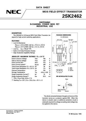
DATA SHEET MOS FIELD EFFECT TRANSISTOR 2SK2462 SWITCHING N-CHANNEL POWER MOS FET INDUSTRIAL USE DESCRIPTION The 2SK2462 is N-Channel MOS Field Effect Transistor de- PACKAGE DIMENSIONS (in millimeters) signed for high current switching applications. 10.0 0.3 4.5 0.2 3.2 0.2 FEATURES 2.7 0.2 Low On-Resistance RDS(on)1 = 0.14 MAX. (@ VGS = 10 V, ID = 8.0 A) RDS(on)2
2sk2413.pdf
DATA SHEET MOS FIELD EFFECT TRANSISTOR 2SK2413 SWITCHING N-CHANNEL POWER MOS FET INDUSTRIAL USE DESCRIPTION PACKAGE DIMENSIONS The 2SK2413 is N-Channel MOS Field Effect Transistor de- (in millimeter) signed for high speed switching applications. FEATURES 4.5 0.2 Low On-Resistance 8.0 0.2 RDS(on)1 = 70 m MAX. (@ VGS = 10 V, ID = 5.0 A) RDS(on)2 = 95 m MAX. (@ VGS =
2sk2400.pdf
2SK2400 2 TOSHIBA Field Effect Transistor Silicon N Channel MOS Type (L - -MOSV) 2SK2400 Chopper Regulator, DC-DC Converter and Motor Drive Unit mm Applications 4 V gate drive Low drain-source ON resistance R = 17 (typ.) DS (ON) High forward transfer admittance Y = 4.5 S (typ.) fs Low leakage current IDSS = 100 A (max) (V = 100 V) DS Enhanceme
2sk2417.pdf
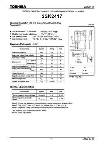
2SK2417 TOSHIBA Field Effect Transistor Silicon N Channel MOS Type ( -MOSV) 2SK2417 Chopper Regulator, DC-DC Converter and Motor Drive Unit mm Applications Low drain-source ON resistance RDS (ON) = 0.42 (typ.) High forward transfer admittance Y = 7.5 S (typ.) fs Low leakage current I = 100 A (max) (V = 250 V) DSS DS Enhancement-mode Vth = 1.5 3.5
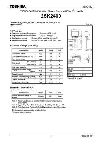
2sk2445.pdf
2SK2445 TOSHIBA Field Effect Transistor Silicon N Channel MOS Type ( -MOSV) 2SK2445 Chopper Regulator, DC-DC Converter and Motor Drive Unit mm Applications Low drain-source ON resistance RDS (ON) = 14 m (typ.) High forward transfer admittance Y = 40 S (typ.) fs Low leakage current I = 100 A (max) (V = 60 V) DSS DS Enhancement-mode Vth = 1.5 3.0 V (
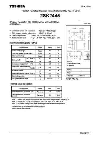
2sk2493.pdf
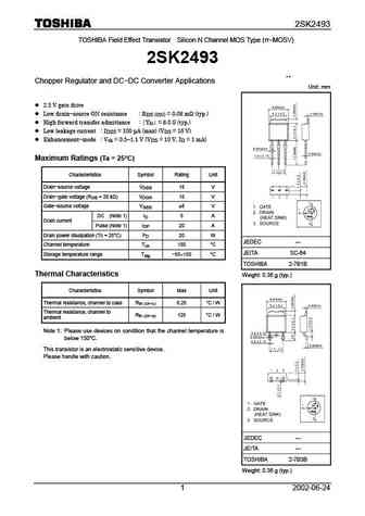
2SK2493 TOSHIBA Field Effect Transistor Silicon N Channel MOS Type ( -MOSV) 2SK2493 Chopper Regulator and DC-DC Converter Applications Unit mm 2.5 V gate drive Low drain-source ON resistance R = 0.08 m (typ.) DS (ON) High forward transfer admittance Y = 8.0 S (typ.) fs Low leakage current IDSS = 100 A (max) (V = 16 V) DS Enhancement-mode V = 0.5
2sk2401.pdf
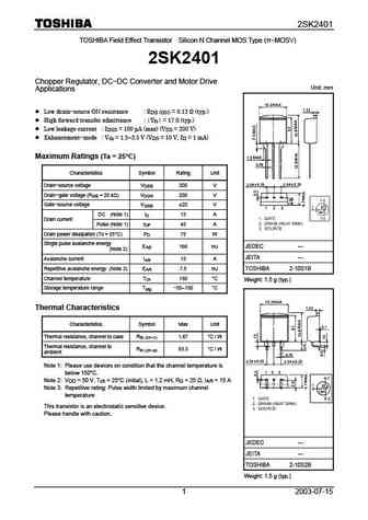
2SK2401 TOSHIBA Field Effect Transistor Silicon N Channel MOS Type ( -MOSV) 2SK2401 Chopper Regulator, DC-DC Converter and Motor Drive Unit mm Applications Low drain-source ON resistance RDS (ON) = 0.13 (typ.) High forward transfer admittance Yfs = 17 S (typ.) Low leakage current IDSS = 100 A (max) (VDS = 200 V) Enhancement-mode Vth = 1.5 3.5 V (VDS =
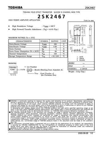
2sk246.pdf
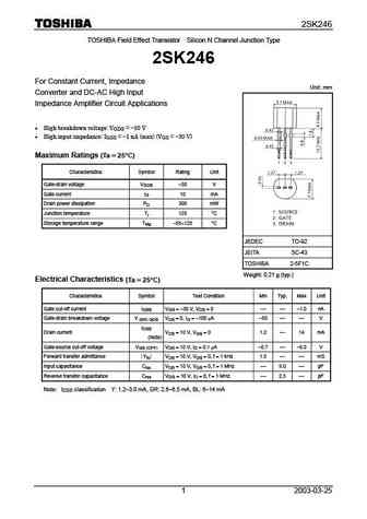
2SK246 TOSHIBA Field Effect Transistor Silicon N Channel Junction Type 2SK246 For Constant Current, Impedance Unit mm Converter and DC-AC High Input Impedance Amplifier Circuit Applications High breakdown voltage VGDS = -50 V High input impedance I = -1 nA (max) (V = -30 V) GSS GS Maximum Ratings (Ta = = 25 C) = = Characteristics Symbol Rating Unit Gate-dra
2sk241.pdf
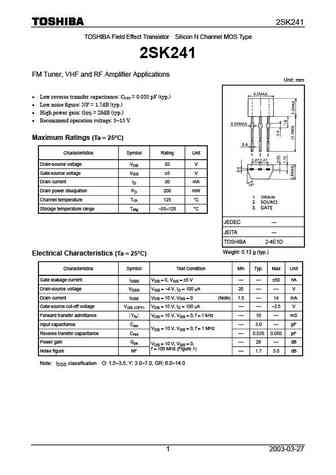
2SK241 TOSHIBA Field Effect Transistor Silicon N Channel MOS Type 2SK241 FM Tuner, VHF and RF Amplifier Applications Unit mm Low reverse transfer capacitance Crss = 0.035 pF (typ.) Low noise figure NF = 1.7dB (typ.) High power gain GPS = 28dB (typ.) Recommend operation voltage 5 15 V Maximum Ratings (Ta = 25 C) Characteristics Symbol Rating Unit Drain
2sk2466.pdf
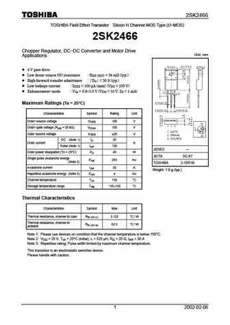
2SK2466 TOSHIBA Field Effect Transistor Silicon N Channel MOS Type (U-MOS) 2SK2466 Chopper Regulator, DC-DC Converter and Motor Drive Unit mm Applications 4 V gate drive Low drain-source ON resistance R = 34 m (typ.) DS (ON) High forward transfer admittance Y = 30 S (typ.) fs Low leakage current IDSS = 100 A (max) (V = 100 V) DS Enhancement-mode
2sk2406.pdf
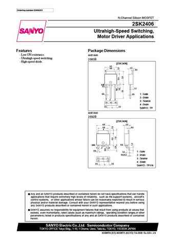
Ordering number ENN5251 N-Channel Silicon MOSFET 2SK2406 Ultrahigh-Speed Switching, Motor Driver Applications Features Package Dimensions Low ON-resistance. unit mm Ultrahigh-speed switching. 2083B High-speed diode. [2SK2406] 6.5 2.3 5.0 0.5 4 0.85 0.7 1.2 0.6 0.5 1 Gate 2 Drain 1 2 3 3 Source 4 Drain 2.3 2.3 SANYO TP unit mm 2092B [2SK2406]
2sk2442.pdf
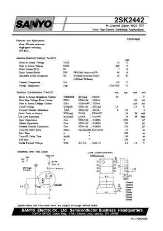
2SK2442 N- Channel Silicon MOS FET Very High-Speed Switching Applications TENTATIVE Features and Applications Low ON-state resistance. high-speed switching. 4V drive. Absolute Maximum Ratings / Ta=25 C unit Drain to Source Voltage VDSS 30 V Gate to Source Voltage VGSS 20 V Drain Current (D.C) ID 7 A Drain Current (Pulse) IDP PW 10 S. dutycycle 1% 48 A Allowable
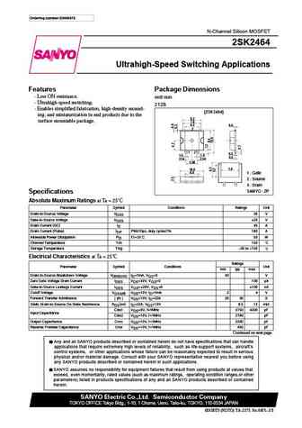
2sk2434.pdf
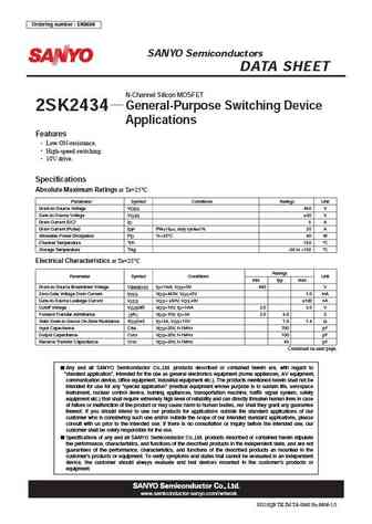
Ordering number EN8606 2SK2434 SANYO Semiconductors DATA SHEET N-Channel Silicon MOSFET General-Purpose Switching Device 2SK2434 Applications Features Low ON-resistance. High-speed switching. 10V drive. Specifications Absolute Maximum Ratings at Ta=25 C Parameter Symbol Conditions Ratings Unit Drain-to-Source Voltage VDSS 450 V Gate-to-Source Voltage VGSS 30 V
2sk2440.pdf
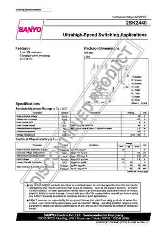
Ordering number ENN5094 N-Channel Silicon MOSFET 2SK2440 Ultrahigh-Speed Switching Applications Features Package Dimensions Low ON resistance. unit mm Ultrahigh-speed switching. 2116 2.5V drive. [2SK2440] 8 5 1 Source 2 Source 3 Source 14 0.2 4 Gate 5.0 5 Drain 6 Drain 7 Drain 8 Drain 0.595 1.27 0.43 SANYO SOP8 Specifications Absolute Maxi
2sk2433.pdf
2SK2433 No. N8353 N MOS 2SK2433 , Absolute Maximum Ratings / Ta=25 uni
2sk2464.pdf
Ordering number ENN6475 N-Channel Silicon MOSFET 2SK2464 Ultrahigh-Speed Switching Applications Features Package Dimensions Low ON resistance. unit mm Ultrahigh-speed switching. 2128 Enables simplified fabrication, high-density mound- [2SK2464] ing, and miniaturization in end products due to the 8.2 surface mountable package. 7.8 6.2 0.6 3 1 2 0.3 1.0 1.0 0.6 2
2sk2441.pdf
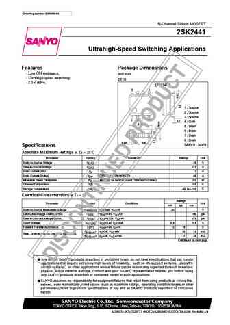
Ordering number ENN4984A N-Channel Silicon MOSFET 2SK2441 Ultrahigh-Speed Switching Applications Features Package Dimensions Low ON resistance. unit mm Ultrahigh-speed switching. 2116 2.5V drive. [2SK2441] 8 5 1 Source 2 Source 3 Source 14 0.2 4 Gate 5.0 5 Drain 6 Drain 7 Drain 8 Drain 0.595 1.27 0.43 SANYO SOP8 Specifications Absolute Max
2sk2403.pdf

Ordering number EN8602 2SK2403 SANYO Semiconductors DATA SHEET N-Channel Silicon MOSFET General-Purpose Switching Device 2SK2403 Applications Features Built-in FRD. 10V drive. Specifications Absolute Maximum Ratings at Ta=25 C Parameter Symbol Conditions Ratings Unit Drain-to-Source Voltage VDSS 450 V Gate-to-Source Voltage VGSS 30 V Drain Current (DC) ID 3 A Drain
2sk242.pdf
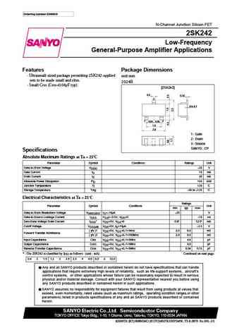
Ordering number EN695G N-Channel Junction Silicon FET 2SK242 Low-Frequency General-Purpose Amplifier Applications Features Package Dimensions Ultrasmall-sized package permitting 2SK242-applied unit mm sets to be made small and slim. 2024B Small Crss (Crss=0.04pF typ). [2SK242] 0.4 0.16 3 0 to 0.1 1 0.95 2 0.95 1.9 2.9 1 Gate 2 Drain 3 Source SANYO CP Spec
2sk2408.pdf
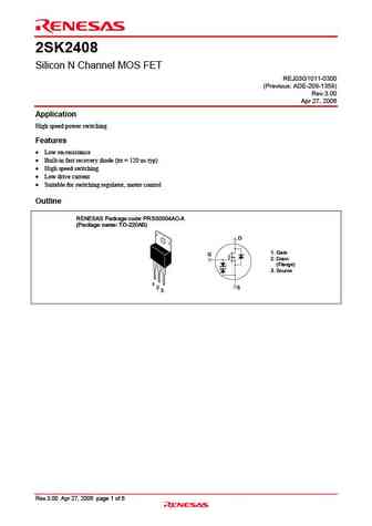
2SK2408 Silicon N Channel MOS FET REJ03G1011-0300 (Previous ADE-208-1358) Rev.3.00 Apr 27, 2006 Application High speed power switching Features Low on-resistance Built-in fast recovery diode (trr = 120 ns typ) High speed switching Low drive current Suitable for switching regulator, motor control Outline RENESAS Package code PRSS0004AC-A (Pack
2sk2499-z.pdf
To our customers, Old Company Name in Catalogs and Other Documents On April 1st, 2010, NEC Electronics Corporation merged with Renesas Technology Corporation, and Renesas Electronics Corporation took over all the business of both companies. Therefore, although the old company name remains in this document, it is a valid Renesas Electronics document. We appreciate your understanding.
2sk2414-z.pdf

To our customers, Old Company Name in Catalogs and Other Documents On April 1st, 2010, NEC Electronics Corporation merged with Renesas Technology Corporation, and Renesas Electronics Corporation took over all the business of both companies. Therefore, although the old company name remains in this document, it is a valid Renesas Electronics document. We appreciate your understanding.
rej03g1011 2sk2408ds.pdf
To our customers, Old Company Name in Catalogs and Other Documents On April 1st, 2010, NEC Electronics Corporation merged with Renesas Technology Corporation, and Renesas Electronics Corporation took over all the business of both companies. Therefore, although the old company name remains in this document, it is a valid Renesas Electronics document. We appreciate your understanding.
2sk2415-z.pdf
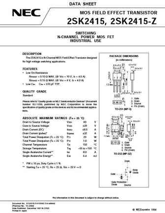
DATA SHEET MOS FIELD EFFECT TRANSISTOR 2SK2415, 2SK2415-Z SWITCHING N-CHANNEL POWER MOS FET INDUSTRIAL USE DESCRIPTION PACKAGE DIMENSIONS The 2SK2415 is N-Channel MOS Field Effect Transistor designed (in millimeters) for high voltage switching applications. 2.3 0.2 6.5 0.2 5.0 0.2 0.5 0.1 FEATURES 4 Low On-Resistance RDS(on)1 = 0.10 MAX. (@ VGS = 10 V, ID =
2sk2485.pdf
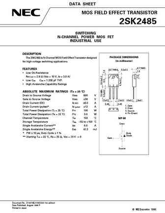
DATA SHEET MOS FIELD EFFECT TRANSISTOR 2SK2485 SWITCHING N-CHANNEL POWER MOS FET INDUSTRIAL USE DESCRIPTION PACKAGE DIMENSIONS The 2SK2485 is N-Channel MOS Field Effect Transistor designed (in millimeter) for high voltage switching applications. 4.7 MAX. FEATURES 15.7 MAX. 3.2 0.2 1.5 Low On-Resistance 4 RDS (on) = 2.8 (VGS = 10 V, ID = 3.0 A) Low Ciss Ciss = 1 20
2sk2484.pdf
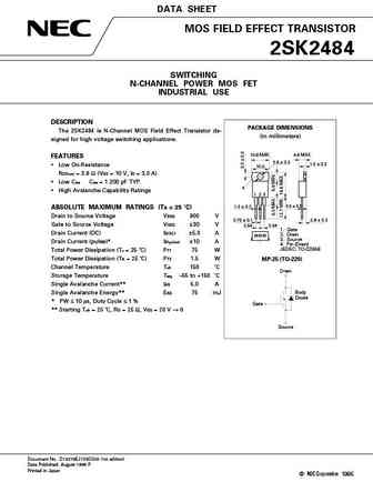
DATA SHEET MOS FIELD EFFECT TRANSISTOR 2SK2484 SWITCHING N-CHANNEL POWER MOS FET INDUSTRIAL USE DESCRIPTION PACKAGE DIMENSIONS The 2SK2484 is N-Channel MOS Field Effect Transistor de- (in millimeters) signed for high voltage switching applications. 10.6 MAX. 4.8 MAX. FEATURES 3.6 0.2 1.3 0.2 Low On-Resistance 10.0 RDS(on) = 2.8 (VGS = 10 V, ID = 3.0 A) Low Ci
2sk2480.pdf
DATA SHEET MOS FIELD EFFECT TRANSISTOR 2SK2480 SWITCHING N-CHANNEL POWER MOS FET INDUSTRIAL USE DESCRIPTION PACKAGE DIMENSIONS The 2SK2480 is N-Channel MOS Field Effect Transistor designed (in millimeter) for high voltage switching applications. FEATURES 10.0 0.3 4.5 0.2 3.2 0.2 Low On-Resistance 2.7 0.2 RDS (on) = 4.0 (VGS = 10 V, ID = 2.0 A) Low Ciss Ciss = 90
2sk2411-z.pdf
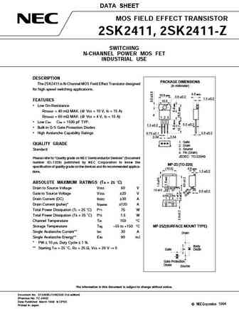
DATA SHEET MOS FIELD EFFECT TRANSISTOR 2SK2411, 2SK2411-Z SWITCHING N-CHANNEL POWER MOS FET INDUSTRIAL USE DESCRIPTION PACKAGE DIMENSIONS The 2SK2411 is N-Channel MOS Field Effect Transistor designed (in millimeter) for high speed switching applications. 4.8 MAX. 10.6 MAX. 3.6 0.2 1.3 0.2 FEATURES 10.0 Low On-Resistance RDS(on)1 = 40 m MAX. (@ VGS = 10 V, ID = 15 A)
2sk2482.pdf

DATA SHEET MOS FIELD EFFECT TRANSISTOR 2SK2482 SWITCHING N-CHANNEL POWER MOS FET INDUSTRIAL USE DESCRIPTION PACKAGE DIMENSIONS The 2SK2482 is N-Channel MOS Field Effect Transistor designed (in millimeter) for high voltage switching applications. FEATURES 4.7 MAX. 15.7 MAX. 3.2 0.2 1.5 Low On-Resistance RDS (on) = 4.0 (VGS = 10 V, ID = 3.0 A) 4 Low Ciss Ciss = 900 pF
2sk2486.pdf
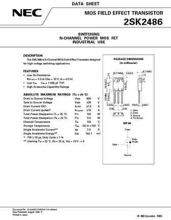
DATA SHEET MOS FIELD EFFECT TRANSISTOR 2SK2486 SWITCHING N-CHANNEL POWER MOS FET INDUSTRIAL USE DESCRIPTION PACKAGE DIMENSIONS The 2SK2486 is N-Channel MOS Field Effect Transistor designed (in millimeter) for high voltage switching applications. FEATURES 4.7 MAX. 15.7 MAX. 3.2 0.2 1.5 Low On-Resistance 4 RDS (on) = 2.0 (VGS = 10 V, ID = 4.0 A) Low Ciss Ciss = 1 830
2sk2483.pdf
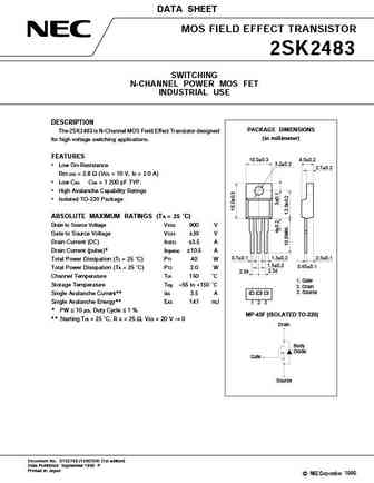
DATA SHEET MOS FIELD EFFECT TRANSISTOR 2SK2483 SWITCHING N-CHANNEL POWER MOS FET INDUSTRIAL USE DESCRIPTION PACKAGE DIMENSIONS The 2SK2483 is N-Channel MOS Field Effect Transistor designed (in millimeter) for high voltage switching applications. FEATURES 10.0 0.3 4.5 0.2 3.2 0.2 Low On-Resistance 2.7 0.2 RDS (on) = 2.8 (VGS = 10 V, ID = 2.0 A) Low Ciss Ciss = 1
2sk2487.pdf
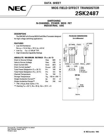
DATA SHEET MOS FIELD EFFECT TRANSISTOR 2SK2487 SWITCHING N-CHANNEL POWER MOS FET INDUSTRIAL USE DESCRIPTION PACKAGE DIMENSIONS The 2SK2487 is N-Channel MOS Field Effect Transistor designed (in millimeter) for high voltage switching applications. FEATURES 4.7 MAX. 15.7 MAX. 3.2 0.2 1.5 Low On-Resistance 4 RDS (on) = 1.6 (VGS = 10 V, ID = 4.0 A) Low Ciss Ciss = 2 100
2sk2481.pdf

DATA SHEET MOS FIELD EFFECT TRANSISTOR 2SK2481 SWITCHING N-CHANNEL POWER MOS FET INDUSTRIAL USE DESCRIPTION PACKAGE DIMENSIONS The 2SK2481 is N-Channel MOS Field Effect Transistor de- (in millimeters) signed for high voltage switching applications. 10.6 MAX. 4.8 MAX. FEATURES 3.6 0.2 1.3 0.2 10.0 Low On-Resistance RDS(on) = 4.0 (VGS = 10 V, ID = 2.0 A) Low Cis
2sk2488.pdf

DATA SHEET MOS FIELD EFFECT TRANSISTOR 2SK2488 SWITCHING N-CHANNEL POWER MOS FET INDUSTRIAL USE DESCRIPTION PACKAGE DIMENSIONS The 2SK2488 is N-Channel MOS Field Effect Transistor designed (in millimeter) for high voltage switching applications. FEATURES 4.7 MAX. 15.7 MAX. 3.2 0.2 Low On-Resistance 1.5 RDS (on) = 1.2 (VGS = 10 V, ID = 5.0 A) 4 Low Ciss Ciss = 2 90
2sk2460n.pdf
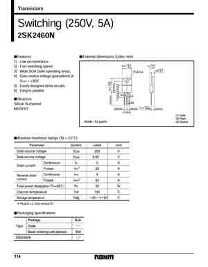
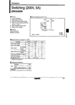
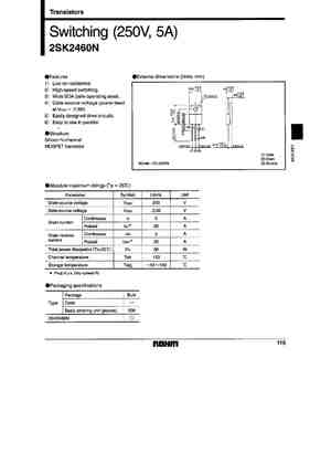
Transistors Switching (250V, 5A) 2SK2460N FFeatures FExternal dimensions (Units mm) 1) Low on-resistance. 2) Fast switching speed. 3) Wide SOA (safe operating area). 4) Gate-source voltage guaranteed at VGSS = 30V. 5) Easily designed drive circuits. 6) Easy to parallel. FStructure Silicon N-channel MOSFET FAbsolute maximum ratings (Ta = 25_C) FPackaging specifications 114
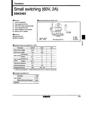
2sk2463.pdf
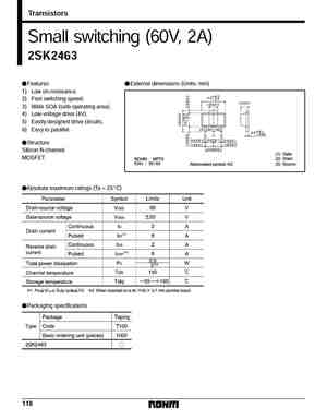
Transistors Small switching (60V, 2A) 2SK2463 FFeatures FExternal dimensions (Units mm) 1) Low on-resistance. 2) Fast switching speed. 3) Wide SOA (safe operating area). 4) Low-voltage drive (4V). 5) Easily designed drive circuits. 6) Easy to parallel. FStructure Silicon N-channel MOSFET FAbsolute maximum ratings (Ta = 25_C) FPackaging specifications 118 Transistors 2SK2463
2sk2474.pdf
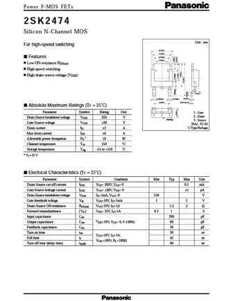
Power F-MOS FETs 2SK2474 2SK2474 Silicon N-Channel MOS Unit mm For high-speed switching 6.5 0.1 5.3 0.1 4.35 0.1 Features 3.0 0.1 Low ON-resistance RDS(on) High-speed switching High drain-source voltage (VDSS) 1.0 0.1 0.85 0.1 0.75 0.1 0.5 0.1 4.6 0.1 0.05 to 0.15 Absolute Maximum Ratings (Tc = 25 C) Parameter Symbol Rating Unit 1 Gate 1 2 3 2 Drai
2sk2495.pdf
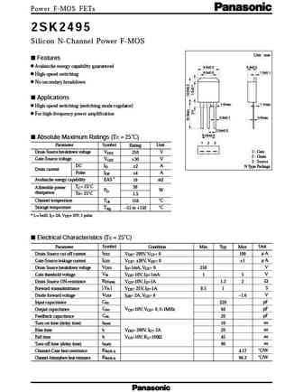
Power F-MOS FETs 2SK2495 2SK2495 Silicon N-Channel Power F-MOS Unit mm Features Avalanche energy capability guaranteed 3.4 0.3 8.5 0.2 6.0 0.5 1.0 0.1 High-speed switching No secondary breakdown Applications 1.5max. 1.1max. High-speed switching (switching mode regulator) For high-frequency power amplification 0.8 0.1 0.5max. 2.54 0.3 5.08 0.5 Absolute Maximu
2sk2431.pdf

2SK2431 Silicon N-Channel MOS FET Application High speed power switching Features Low on-resistance High speed switching Low drive current No Secondary Breakdown Suitable for Switching regulator, DC-DC converter. Outline TO-220CFM 1 D 2 3 1. Gate G 2. Drain 3. Source S 2SK2431 Absolute Maximum Ratings (Ta = 25 C) Item Symbol Ratings Unit Drain to so
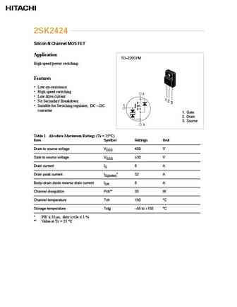
2sk2425.pdf
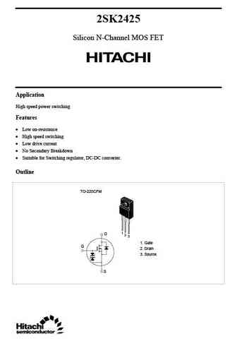
2SK2425 Silicon N-Channel MOS FET Application High speed power switching Features Low on-resistance High speed switching Low drive current No Secondary Breakdown Suitable for Switching regulator, DC-DC converter. Outline TO-220CFM 1 D 2 3 1. Gate G 2. Drain 3. Source S 2SK2425 Absolute Maximum Ratings (Ta = 25 C) Item Symbol Ratings Unit Drain to so
2sk1637 2sk2422.pdf
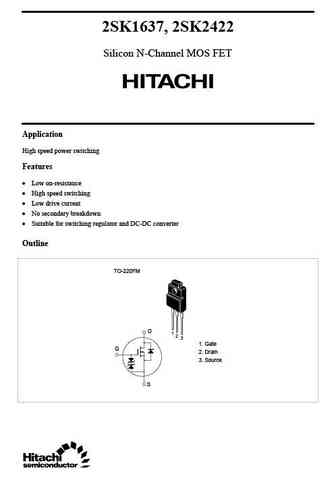
2SK1637, 2SK2422 Silicon N-Channel MOS FET Application High speed power switching Features Low on-resistance High speed switching Low drive current No secondary breakdown Suitable for switching regulator and DC-DC converter Outline TO-220FM D 1 2 3 1. Gate G 2. Drain 3. Source S 2SK1637, 2SK2422 Absolute Maximum Ratings (Ta = 25 C) Item Symbol Rating
2sk2423.pdf

2SK2423 Silicon N-Channel MOS FET Application High speed power switching Features Low on-resistance High speed switching Low drive current No Secondary Breakdown Suitable for Switching regulator, DC-DC converter. Outline TO-220CFM 1 D 2 3 1. Gate G 2. Drain 3. Source S 2SK2423 Absolute Maximum Ratings (Ta = 25 C) Item Symbol Ratings Unit Drain to so
2sk2426.pdf

2SK2426 Silicon N-Channel MOS FET Application High speed power switching Features Low on-resistance High speed switching Low drive current No Secondary Breakdown Suitable for Switching regulator, DC-DC converter. Outline TO-220CFM 1 D 2 3 1. Gate G 2. Drain 3. Source S 2SK2426 Absolute Maximum Ratings (Ta = 25 C) Item Symbol Ratings Unit Drain to so
3sk73 3sk77 2sk240 2sj75 2sk146 2sj73 2sk389 2sj109 2sk266 2sk455 2sk456 2sc3381 2sa1349.pdf
www.DataSheet4U.com
2sk2421.pdf
2SK2421 External dimensions 1 ...... FM20 Absolute Maximum Ratings Electrical Characteristics (Ta = 25 C) (Ta = 25 C) Ratings Symbol Ratings Unit Symbol Unit Conditions min typ max V 60 V V 60 V I = 100 A, V = 0V DSS (BR) DSS D GS V 20 V I 100 nA V = 20V GSS GSS GS I 40 A I 100 A V = 60V, V = 0V D DSS DS GS I 160 A V 2.0 4.0 V V = 10V, I = 1mA D (pulse) TH DS D
2sk2420.pdf
2SK2420 External dimensions 1 ...... FM20 Absolute Maximum Ratings Electrical Characteristics (Ta = 25 C) (Ta = 25 C) Ratings Symbol Ratings Unit Symbol Unit Conditions min typ max V 60 V V 60 V I = 100 A, V = 0V DSS (BR) DSS D GS V 20 V I 100 nA V = 20V GSS GSS GS I 30 A I 100 A V = 60V, V = 0V D DSS DS GS I 120 A V 2.0 4.0 V V = 10V, I = 250 A D (pulse) TH DS
2sk1871 2sk2153 2sk2164 2sk2321 2sk2432 2sk2435 2sk2436 2sk2438 2sk2439 2sk2626 2sk2634 2sk2635 2sk2636 2sk2637 2sk2773.pdf
2sk2420.pdf
2SK2420 External dimensions 1 ...... FM20 Absolute Maximum Ratings Electrical Characteristics (Ta = 25 C) (Ta = 25 C) Ratings Symbol Ratings Unit Symbol Unit Conditions min typ max V 60 V V 60 V I = 100 A, V = 0V DSS (BR) DSS D GS V 20 V I 100 nA V = 20V GSS GSS GS I 30 A I 100 A V = 60V, V = 0V D DSS DS GS I 120 A V 2.0 4.0 V V = 10V, I = 250 A D (pulse) TH DS
2sk2489.pdf
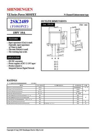
SHINDENGEN VZ Series Power MOSFET N-Channel Enhancement type OUTLINE DIMENSIONS 2SK2489 Case STO-220 (Unit mm) ( F10S18VZ ) 180V 10A FEATURES Input capacitance (Ciss) is small. Especially, input capacitance at 0 biass is small. The static Rds(on) is small. The switching time is fast. APPLICATION DC/DC converters Power supplies of DC 12-24V input Pr
2sk2475 f12f50vx2.pdf
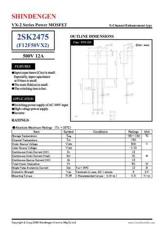
SHINDENGEN VX-2 Series Power MOSFET N-Channel Enhancement type OUTLINE DIMENSIONS 2SK2475 Case FTO-220 (Unit mm) (F12F50VX2) 500V 12A FEATURES Input capacitance (Ciss) is small. Especially, input capacitance at 0 biass is small. The static Rds(on) is small. The switching time is fast. APPLICATION Switching power supply of AC 100V input High voltage power supply Inverter
2sk2414.pdf
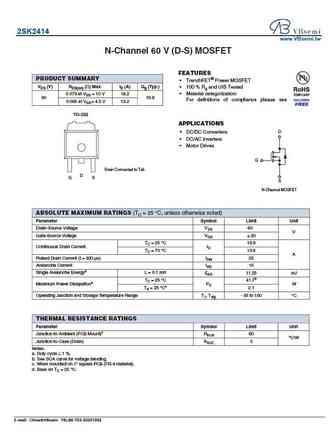
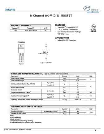
2SK2414 www.VBsemi.tw N-Channel 60 V (D-S) MOSFET FEATURES PRODUCT SUMMARY TrenchFET Power MOSFET VDS (V) RDS(on) ( ) Max. ID (A) Qg (Typ.) 100 % Rg and UIS Tested 0.073 at VGS = 10 V 18.2 Material categorization 60 19.8 For definitions of compliance please see 0.085 at VGS = 4.5 V 13.2 TO-252 APPLICATIONS D DC/DC Converters DC/AC Inverters Motor
2sk2498.pdf
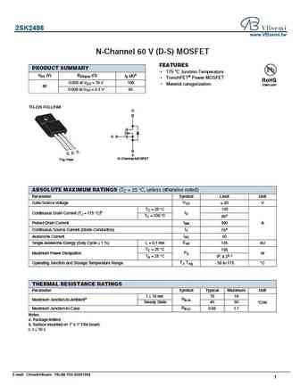
2SK2498 www.VBsemi.tw N-Channel 60 V (D-S) MOSFET FEATURES PRODUCT SUMMARY 175 C Junction Temperature VDS (V) RDS(on) ( ) ID (A)a TrenchFET Power MOSFET 0.005 at VGS = 10 V 100 Material categorization 60 0.008 at VGS = 4.5 V 95 TO-220 FULLPAK D G S D G S N-Channel MOSFET Top View ABSOLUTE MAXIMUM RATINGS (TC = 25 C, unless otherwise noted) Paramete
2sk2462.pdf
2SK2462 www.VBsemi.tw N-Channel 100-V (D-S) MOSFET FEATURES PRODUCT SUMMARY TrenchFET Power MOSFET V(BR)DSS (V) RDS(on) ( )ID (A) 175 C Junction Temperature RoHS 0.092 at VGS = 10 V 100 18 COMPLIANT Low Thermal Resistance Package 100 % Rg Tested APPLICATIONS Isolated DC/DC Converters TO-220AB D G S G D S N-Channel MOSFET Top View ABSOLUTE MAXI
2sk2424.pdf
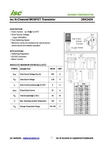
isc N-Channel MOSFET Transistor 2SK2424 DESCRIPTION Drain Current I = 8A@ T =25 D C Drain Source Voltage- V = 450V(Min) DSS Fast Switching Speed Minimum Lot-to-Lot variations for robust device performance and reliable operation APPLICATIONS Switching Regulators DC-DC Converter, Motor Control ABSOLUTE MAXIMUM RATINGS(T =25 ) a SYMBOL ARAMETER VALUE UNIT V Dr
2sk2402.pdf
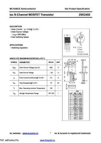
INCHANGE Semiconductor isc Product Specification isc N-Channel MOSFET Transistor 2SK2402 DESCRIPTION Drain Current ID= 3.5A@ TC=25 Drain Source Voltage- VDSS= 600V(Min) Fast Switching Speed APPLICATIONS Switching regulators ABSOLUTE MAXIMUM RATINGS(Ta=25 ) SYMBOL VALUE UNIT ARAMETER VDSS Drain-Source Voltage (VGS=0) 600 V VGS Gate-Source Voltage 30 V
2sk2417.pdf

isc N-Channel MOSFET Transistor 2SK2417 DESCRIPTION Drain Current I = 7.5A@ T =25 D C Drain Source Voltage- V = 250V(Min) DSS Fast Switching Speed Minimum Lot-to-Lot variations for robust device performance and reliable operation APPLICATIONS Switching Regulators DC-DC Converter, Motor Control ABSOLUTE MAXIMUM RATINGS(T =25 ) a SYMBOL ARAMETER VALUE UNIT V
2sk2408.pdf
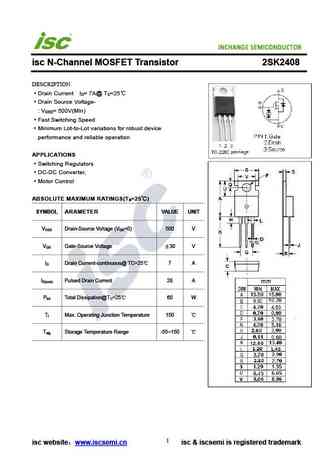
isc N-Channel MOSFET Transistor 2SK2408 DESCRIPTION Drain Current I = 7A@ T =25 D C Drain Source Voltage- V = 500V(Min) DSS Fast Switching Speed Minimum Lot-to-Lot variations for robust device performance and reliable operation APPLICATIONS Switching Regulators DC-DC Converter, Motor Control ABSOLUTE MAXIMUM RATINGS(T =25 ) a SYMBOL ARAMETER VALUE UNIT V Dr
2sk2431.pdf
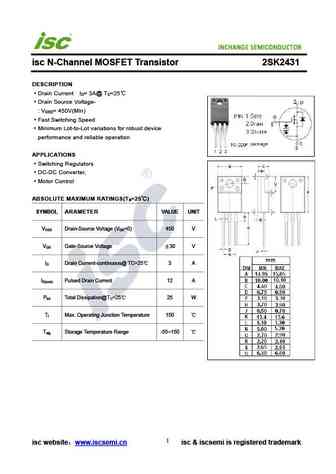
isc N-Channel MOSFET Transistor 2SK2431 DESCRIPTION Drain Current I = 3A@ T =25 D C Drain Source Voltage- V = 450V(Min) DSS Fast Switching Speed Minimum Lot-to-Lot variations for robust device performance and reliable operation APPLICATIONS Switching Regulators DC-DC Converter, Motor Control ABSOLUTE MAXIMUM RATINGS(T =25 ) a SYMBOL ARAMETER VALUE UNIT V Dr
2sk2401.pdf
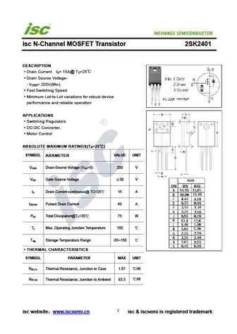
isc N-Channel MOSFET Transistor 2SK2401 DESCRIPTION Drain Current I = 15A@ T =25 D C Drain Source Voltage- V = 200V(Min) DSS Fast Switching Speed Minimum Lot-to-Lot variations for robust device performance and reliable operation APPLICATIONS Switching Regulators DC-DC Converter, Motor Control ABSOLUTE MAXIMUM RATINGS(T =25 ) a SYMBOL ARAMETER VALUE UNIT V D
2sk2420.pdf
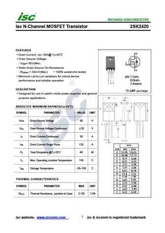
isc N-Channel MOSFET Transistor 2SK2420 FEATURES Drain Current I = 30A@ T =25 D C Drain Source Voltage- V = 60V(Min) DSS Static Drain-Source On-Resistance R = 28m (Max) 100% avalanche tested DS(on) Minimum Lot-to-Lot variations for robust device performance and reliable operation DESCRIPTION Designed for use in switch mode power supplies and general purpose
2sk2485.pdf
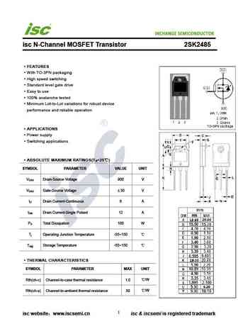
INCHANGE Semiconductor isc N-Channel MOSFET Transistor 2SK2485 FEATURES With TO-3PN packaging High speed switching Standard level gate drive Easy to use 100% avalanche tested Minimum Lot-to-Lot variations for robust device performance and reliable operation APPLICATIONS Power supply Switching applications ABSOLUTE MAXIMUM RATINGS(T =25 ) a SYMBOL PARAMETER
2sk2407.pdf
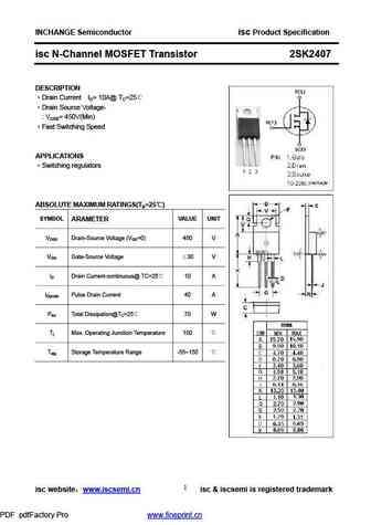
INCHANGE Semiconductor isc Product Specification isc N-Channel MOSFET Transistor 2SK2407 DESCRIPTION Drain Current ID= 10A@ TC=25 Drain Source Voltage- VDSS= 450V(Min) Fast Switching Speed APPLICATIONS Switching regulators ABSOLUTE MAXIMUM RATINGS(Ta=25 ) SYMBOL VALUE UNIT ARAMETER VDSS Drain-Source Voltage (VGS=0) 450 V VGS Gate-Source Voltage 30 V
2sk2461.pdf
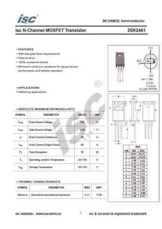
INCHANGE Semiconductor isc N-Channel MOSFET Transistor 2SK2461 FEATURES With low gate drive requirements Easy to drive 100% avalanche tested Minimum Lot-to-Lot variations for robust device performance and reliable operation APPLICATIONS Switching applications ABSOLUTE MAXIMUM RATINGS(T =25 ) a SYMBOL PARAMETER VALUE UNIT V Drain-Source Voltage 100 V DSS V Gate-S
2sk2425.pdf
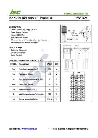
isc N-Channel MOSFET Transistor 2SK2425 DESCRIPTION Drain Current I = 7A@ T =25 D C Drain Source Voltage- V = 250V(Min) DSS Fast Switching Speed Minimum Lot-to-Lot variations for robust device performance and reliable operation APPLICATIONS Switching Regulators DC-DC Converter, Motor Control ABSOLUTE MAXIMUM RATINGS(T =25 ) a SYMBOL ARAMETER VALUE UNIT V Dr
2sk2475.pdf
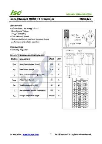
isc N-Channel MOSFET Transistor 2SK2475 DESCRIPTION Drain Current I = 12A@ T =25 D C Drain Source Voltage- V = 500V(Min) DSS Fast Switching Speed Minimum Lot-to-Lot variations for robust device performance and reliable operation APPLICATIONS Switching Regulators ABSOLUTE MAXIMUM RATINGS(T =25 ) a SYMBOL ARAMETER VALUE UNIT V Drain-Source Voltage (V =0) 500 V DSS
2sk2423.pdf
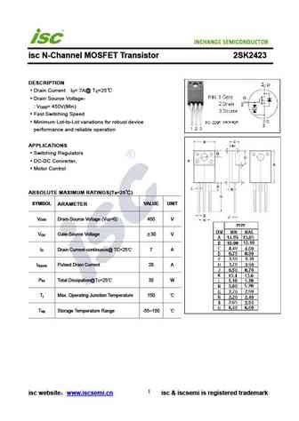
isc N-Channel MOSFET Transistor 2SK2423 DESCRIPTION Drain Current I = 7A@ T =25 D C Drain Source Voltage- V = 450V(Min) DSS Fast Switching Speed Minimum Lot-to-Lot variations for robust device performance and reliable operation APPLICATIONS Switching Regulators DC-DC Converter, Motor Control ABSOLUTE MAXIMUM RATINGS(T =25 ) a SYMBOL ARAMETER VALUE UNIT V Dr
Другие IGBT... 2SK2579, 2SK2580, 2SK2581, 2SK2588, 2SK2593, 2SK2406, 2SK242, 2SK2441, AO4407A, 2SK2460N, 2SK2463, 2SK2464, 2SK2474, 2SK2495, 2SJ191, 2SJ192, 2SJ193
🌐 : EN ES РУ

Список транзисторов
Обновления
MOSFET: FTF30P35D | FTF25N35DHVT | FTF15N35D | FTE15C35G | FTP02P15G | FTE02P15G | AKF30N5P0SX | AKF30N10S | AKF20P45D | CM4407 | CM3407 | CM3400 | SVF11N65F | SVF11N65T | FKBB3105 | EHBA036R1
Popular searches
2sa934 | 2sd118 | 2n3403 | 2sa750 | tip117 | 2n3643 | 2sc2078 transistor equivalent | 2sc2073