SSF2302. Аналоги и основные параметры
Наименование производителя: SSF2302
Тип транзистора: MOSFET
Полярность: N
Предельные значения
Pd ⓘ - Максимальная рассеиваемая мощность: 0.9 W
|Vds|ⓘ - Максимально допустимое напряжение сток-исток: 20 V
|Vgs|ⓘ - Максимально допустимое напряжение затвор-исток: 8 V
|Id| ⓘ - Максимально допустимый постоянный ток стока: 2.4 A
Tj ⓘ - Максимальная температура канала: 150 °C
Электрические характеристики
tr ⓘ - Время нарастания: 55 ns
Cossⓘ - Выходная емкость: 120 pf
RDSonⓘ - Сопротивление сток-исток открытого транзистора: 0.06 Ohm
Тип корпуса: SOT23
Аналог (замена) для SSF2302
- подборⓘ MOSFET транзистора по параметрам
SSF2302 даташит
ssf2302.pdf
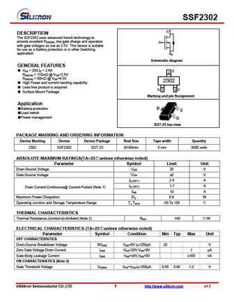
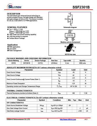
SSF2302 D DESCRIPTION The SSF2302 uses advanced trench technology to provide excellent RDS(ON), low gate charge and operation G with gate voltages as low as 2.5V. This device is suitable for use as a Battery protection or in other Switching application. S Schematic diagram GENERAL FEATURES VDS = 20V,ID = 2.4A D 3 RDS(ON)
ssf2300.pdf
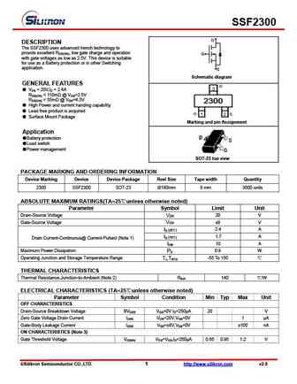
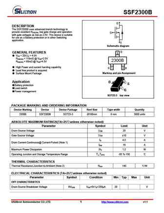
SSF2300 D DESCRIPTION The SSF2300 uses advanced trench technology to provide excellent RDS(ON), low gate charge and operation G with gate voltages as low as 2.5V. This device is suitable for use as a Battery protection or in other Switching application. S Schematic diagram GENERAL FEATURES VDS = 20V,ID = 2.4A RDS(ON)
ssf2300a.pdf
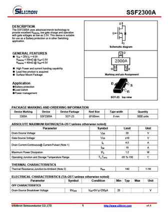
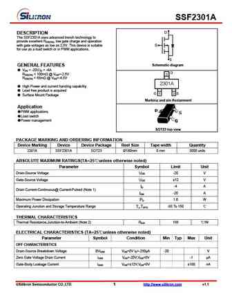
SSF2300A D DESCRIPTION The SSF2300A uses advanced trench technology to provide excellent RDS(ON), low gate charge and operation G with gate voltages as low as 2.5V. This device is suitable for use as a Battery protection or in other Switching application. S Schematic diagram GENERAL FEATURES VDS = 20V,ID = 4.5A RDS(ON)
ssf2306.pdf
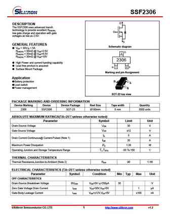
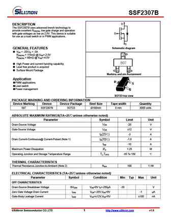
SSF2306 D DESCRIPTION The SSF2306 uses advanced trench technology to provide excellent RDS(ON), G low gate charge and operation with gate voltages as low as 2.5V. S GENERAL FEATURES Schematic diagram VDS = 30V,ID = 5A RDS(ON)
Другие IGBT... SSF2145CH6, SSF2160G4, SSF2300, SSF2300A, SSF2300B, SSF2301, SSF2301A, SSF2301B, IRFP250N, SSF2305, SSF2306, SSF2307B, SSF2312, SSF2314, SSF2316E, SSF2318E, SSF2336
🌐 : EN ES РУ

Список транзисторов
Обновления
MOSFET: FTF30P35D | FTF25N35DHVT | FTF15N35D | FTE15C35G | FTP02P15G | FTE02P15G | AKF30N5P0SX | AKF30N10S | AKF20P45D | CM4407 | CM3407 | CM3400 | SVF11N65F | SVF11N65T | FKBB3105 | EHBA036R1
Popular searches
2sd287 | 2sd438 | a1492 | hy4008 | ncep039n10m | 20n50 | 2sc869 | tip29 transistor equivalent