SSF3051G7. Аналоги и основные параметры
Наименование производителя: SSF3051G7
Тип транзистора: MOSFET
Полярность: P
Предельные значения
Pd ⓘ - Максимальная рассеиваемая мощность: 1.7 W
|Vds|ⓘ - Максимально допустимое напряжение сток-исток: 30 V
|Vgs|ⓘ - Максимально допустимое напряжение затвор-исток: 30 V
|Id| ⓘ - Максимально допустимый постоянный ток стока: 4 A
Tj ⓘ - Максимальная температура канала: 150 °C
Электрические характеристики
tr ⓘ - Время нарастания: 4 ns
Cossⓘ - Выходная емкость: 94 pf
RDSonⓘ - Сопротивление сток-исток открытого транзистора: 0.051 Ohm
Тип корпуса: SOT23-6
Аналог (замена) для SSF3051G7
- подборⓘ MOSFET транзистора по параметрам
SSF3051G7 даташит
ssf3051g7.pdf
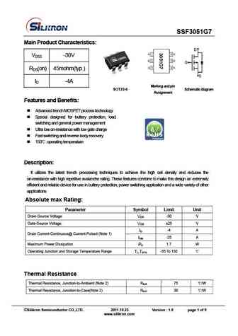
SSF3051G7 Main Product Characteristics D VDSS -30V G RDS(on) 45mohm(typ.) S ID -4A Marking and pin SOT23-6 Schematic diagram Assignment Features and Benefits Advanced trench MOSFET process technology Special designed for buttery protection, load switching and general power management Ultra low on-resistance with low gate charge Fast switching and rev
ssf3056c.pdf
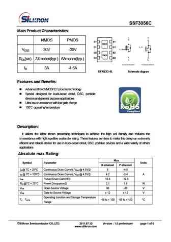
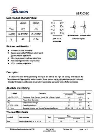
SSF3056C Main Product Characteristics NMOS PMOS D1 S1 D1 S1 NMOS NMOS D1 G1 D1 G1 VDSS 30V -30V D2 S2 D2 S2 PMOS PMOS D2 G2 D2 G2 RDS(on) 37mohm(typ.) 68mohm(typ.) ID 5A -4.5A DFN2X3-8L Schematic diagram Bottom View Features and Benefits Advanced trench MOSFET process technology Special designed for buck-boost circuit, DSC, portable devices and gene
ssf3055.pdf
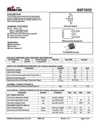
SSF3055 D DESCRIPTION The SSF3055 uses advanced trench technology to provide excellent RDS(ON) and low gate charge. This G device is suitable for use as a Battery protection or in other Switching application. S Schematic diagram GENERAL FEATURES VDS = 25V,ID = 12A RDS(ON)
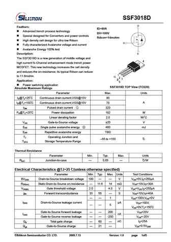
ssf3018.pdf
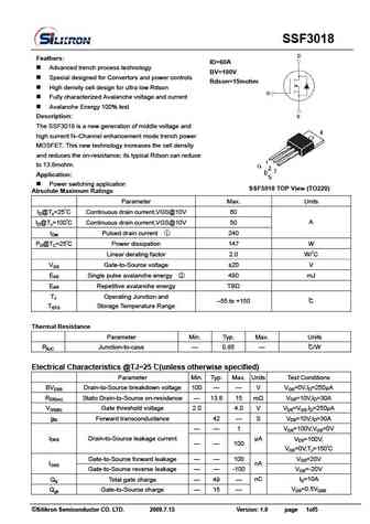
SSF3018 Feathers ID=60A Advanced trench process technology BV=100V Special designed for Convertors and power controls Rdson=15mohm High density cell design for ultra low Rdson Fully characterized Avalanche voltage and current Avalanche Energy 100% test Description The SSF3018 is a new generation of middle voltage and high current N Channel enhancement mode t
Другие IGBT... SSF2N60D2, SSF2N60F, SSF2N60G, SSF3002EG1, SSF3018, SSF3018D, SSF3028C1, SSF3036C, AO3407, SSF3055, SSF3056C, SSF3092G1, SSF3117, SSF32E0E, SSF3314E, SSF3322, SSF3324
History: SSF3055
🌐 : EN ES РУ

Список транзисторов
Обновления
MOSFET: FTF30P35D | FTF25N35DHVT | FTF15N35D | FTE15C35G | FTP02P15G | FTE02P15G | AKF30N5P0SX | AKF30N10S | AKF20P45D | CM4407 | CM3407 | CM3400 | SVF11N65F | SVF11N65T | FKBB3105 | EHBA036R1
Popular searches
2sc1318 datasheet | 2sc3281 datasheet | 2sa1106 | 2sb56 | 2sc1451 datasheet | 2sc373 | a1023 datasheet | 2sc1080