SSF3339. Аналоги и основные параметры
Наименование производителя: SSF3339
Тип транзистора: MOSFET
Полярность: P
Предельные значения
Pd ⓘ - Максимальная рассеиваемая мощность: 1 W
|Vds|ⓘ - Максимально допустимое напряжение сток-исток: 30 V
|Vgs|ⓘ - Максимально допустимое напряжение затвор-исток: 20 V
|Id| ⓘ - Максимально допустимый постоянный ток стока: 4.1 A
Tj ⓘ - Максимальная температура канала: 150 °C
Электрические характеристики
tr ⓘ - Время нарастания: 4.8 ns
Cossⓘ - Выходная емкость: 108 pf
RDSonⓘ - Сопротивление сток-исток открытого транзистора: 0.052 Ohm
Тип корпуса: SOT23
Аналог (замена) для SSF3339
- подборⓘ MOSFET транзистора по параметрам
SSF3339 даташит
ssf3339.pdf
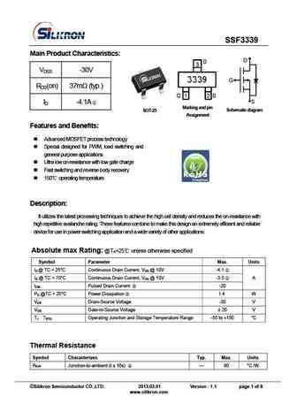
SSF3339 Main Product Characteristics D VDSS -30V G RDS(on) 37m (typ.) S ID -4.1A Marking and pin SOT-23 Schematic diagram Assignme nt Features and Benefits Advanced MOSFET process technology Special designed for PWM, load switching and general purpose applications Ultra low on-resistance with low gate charge Fast switching and reverse body
ssf3338.pdf
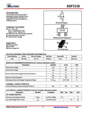
SSF3338 D DESCRIPTION The SSF3338 uses advanced trench technology to provide excellent RDS(ON) G and low gate charge .This device is suitable for use as a load switch or in PWM applications. S Schematic diagram GENERAL FEATURES VDS = 30V,ID =4A RDS(ON)
ssf3341.pdf
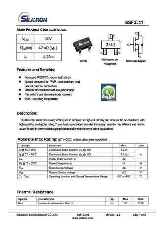
SSF3341 Main Product Characteristics D VDSS -30V G RDS(on) 42m (typ.) S ID -4.2A Marking and pin SOT-23 Schematic diagram Assignme nt Features and Benefits Advanced MOSFET process technology Special designed for PWM, load switching and general purpose applications Ultra low on-resistance with low gate charge Fast switching and reverse body
ssf3341l.pdf

SSF3341L D DESCRIPTION The SSF3341L uses advanced trench technology to provide excellent RDS(ON), low gate charge and operation with gate voltages as low as 2.5V. This device is suitable G for use as a load switch or in PWM applications. S GENERAL FEATURES Schematic diagram VDS = -30V,ID = -4.2A RDS(ON)
Другие IGBT... SSF3056C, SSF3092G1, SSF3117, SSF32E0E, SSF3314E, SSF3322, SSF3324, SSF3338, 75N75, SSF3341, SSF3341L, SSF3365, SSF3402, SSF3416, SSF3420, SSF3428, SSF3604
🌐 : EN ES РУ

Список транзисторов
Обновления
MOSFET: FTF30P35D | FTF25N35DHVT | FTF15N35D | FTE15C35G | FTP02P15G | FTE02P15G | AKF30N5P0SX | AKF30N10S | AKF20P45D | CM4407 | CM3407 | CM3400 | SVF11N65F | SVF11N65T | FKBB3105 | EHBA036R1
Popular searches
2sc1845 transistor | a933 transistor datasheet | a1633 transistor | 2sa844 | 2sc1327 | 2sc3855 | 2sc945 transistor equivalent | 2sd427