SSF3365. Аналоги и основные параметры
Наименование производителя: SSF3365
Тип транзистора: MOSFET
Полярность: P
Предельные значения
Pd ⓘ - Максимальная рассеиваемая мощность: 1.25 W
|Vds|ⓘ - Максимально допустимое напряжение сток-исток: 30 V
|Vgs|ⓘ - Максимально допустимое напряжение затвор-исток: 20 V
|Id| ⓘ - Максимально допустимый постоянный ток стока: 3 A
Tj ⓘ - Максимальная температура канала: 150 °C
Электрические характеристики
tr ⓘ - Время нарастания: 9 ns
Cossⓘ - Выходная емкость: 150 pf
RDSonⓘ - Сопротивление сток-исток открытого транзистора: 0.08 Ohm
Тип корпуса: SOT23
Аналог (замена) для SSF3365
- подборⓘ MOSFET транзистора по параметрам
SSF3365 даташит
ssf3365.pdf
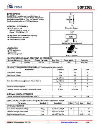
SSF3365 D DESCRIPTION The SSF3365 uses advanced trench technology to provide excellent RDS(ON), low gate charge and operation with gate voltages as low as 2.5V. This device is suitable G for use as a load switch or in PWM applications. S GENERAL FEATURES Schematic diagram VDS = -30V,ID = -3A RDS(ON)
ssf3341.pdf
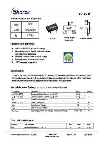
SSF3341 Main Product Characteristics D VDSS -30V G RDS(on) 42m (typ.) S ID -4.2A Marking and pin SOT-23 Schematic diagram Assignme nt Features and Benefits Advanced MOSFET process technology Special designed for PWM, load switching and general purpose applications Ultra low on-resistance with low gate charge Fast switching and reverse body
ssf3341l.pdf

SSF3341L D DESCRIPTION The SSF3341L uses advanced trench technology to provide excellent RDS(ON), low gate charge and operation with gate voltages as low as 2.5V. This device is suitable G for use as a load switch or in PWM applications. S GENERAL FEATURES Schematic diagram VDS = -30V,ID = -4.2A RDS(ON)
ssf3324.pdf
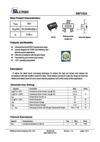
SSF3324 Main Product Characteristics VDSS 30V RDS(on) 26.5mohm(typ.) ID 5.8A Marking and pin SOT23 Schematic diagram Assignme nt Features and Benefits Advanced trench MOSFET process technology Special designed for PWM, load switching and general purpose applications Ultra low on-resistance with low gate charge Fast switching and reverse body rec
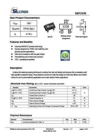
Другие IGBT... SSF32E0E, SSF3314E, SSF3322, SSF3324, SSF3338, SSF3339, SSF3341, SSF3341L, STP65NF06, SSF3402, SSF3416, SSF3420, SSF3428, SSF3604, SSF3605S, SSF3606, SSF3610
🌐 : EN ES РУ

Список транзисторов
Обновления
MOSFET: FTF30P35D | FTF25N35DHVT | FTF15N35D | FTE15C35G | FTP02P15G | FTE02P15G | AKF30N5P0SX | AKF30N10S | AKF20P45D | CM4407 | CM3407 | CM3400 | SVF11N65F | SVF11N65T | FKBB3105 | EHBA036R1
Popular searches
2sa844 | 2sc1327 | 2sc3855 | 2sc945 transistor equivalent | 2sd427 | mje15032 equivalent | 2sc4834 | 2sd313 transistor equivalent