SSF3641. Аналоги и основные параметры
Наименование производителя: SSF3641
Тип транзистора: MOSFET
Полярность: P
Предельные значения
Pd ⓘ
- Максимальная рассеиваемая мощность: 2 W
|Vds|ⓘ - Максимально допустимое напряжение сток-исток: 30 V
|Vgs|ⓘ - Максимально допустимое напряжение затвор-исток: 12 V
|Id| ⓘ - Максимально допустимый постоянный ток стока: 5 A
Tj ⓘ - Максимальная температура канала: 150 °C
Электрические характеристики
tr ⓘ -
Время нарастания: 5 ns
Cossⓘ - Выходная емкость: 100 pf
RDSonⓘ - Сопротивление сток-исток открытого транзистора: 0.049 Ohm
Тип корпуса: SOP8
Аналог (замена) для SSF3641
- подборⓘ MOSFET транзистора по параметрам
SSF3641 даташит
..1. Size:498K silikron
ssf3641.pdf 
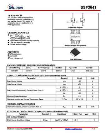
SSF3641 DESCRIPTION The SSF3641 uses advanced trench technology to provide excellent RDS(ON) and low gate charge .This device is suitable for use as a load switch or in PWM applications. Schematic diagram GENERAL FEATURES VDS =- 30V,ID =-5A RDS(ON)
9.1. Size:508K silikron
ssf3624.pdf 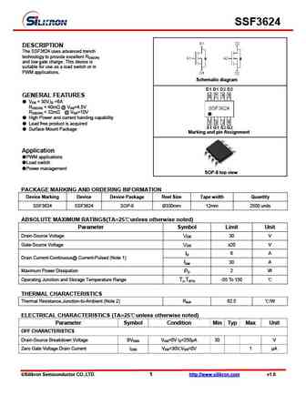
SSF3624 DESCRIPTION The SSF3624 uses advanced trench technology to provide excellent RDS(ON) and low gate charge .This device is suitable for use as a load switch or in PWM applications. Schematic diagram GENERAL FEATURES VDS = 30V,ID =6A RDS(ON)
9.2. Size:472K silikron
ssf3605s.pdf 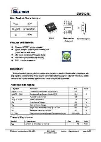
SSF3605S Main Product Characteristics D VDSS -30V G RDS(on) 5.1m (typ.) S ID -15A SOP-8 Mar ki ng a nd p in Schematic diagram Assignment Features and Benefits Advanced MOSFET process technology Special designed for PWM, load switching and general purpose applications Ultra low on-resistance with low gate charge Fast switching and reverse body reco
9.3. Size:442K silikron
ssf3612.pdf 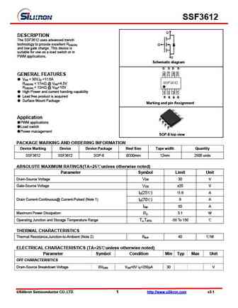
SSF3612 D DESCRIPTION The SSF3612 uses advanced trench technology to provide excellent RDS(ON) G and low gate charge .This device is suitable for use as a load switch or in PWM applications. S Schematic diagram GENERAL FEATURES VDS = 30V,ID =11.6A RDS(ON)
9.4. Size:587K silikron
ssf3616.pdf 
SSF3616 D DESCRIPTION The SSF3616 uses advanced trench technology to provide excellent RDS(ON) G and low gate charge .This device is suitable for use as a load switch or in PWM applications. S Schematic diagram GENERAL FEATURES VDS = 30V,ID =9A RDS(ON)
9.5. Size:327K silikron
ssf3617.pdf 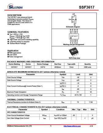
SSF3617 D DESCRIPTION The SSF3617 uses advanced trench technology to provide excellent RDS(ON) G and low gate charge .This device is suitable for use as a load switch or in PWM applications. S Schematic diagram GENERAL FEATURES VDS =-30V,ID =-10A RDS(ON)
9.6. Size:505K silikron
ssf3606.pdf 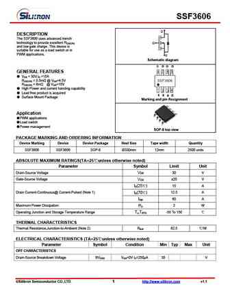
SSF3606 D DESCRIPTION The SSF3606 uses advanced trench technology to provide excellent RDS(ON) G and low gate charge .This device is suitable for use as a load switch or in PWM applications. S Schematic diagram GENERAL FEATURES VDS = 30V,ID =15A RDS(ON)
9.7. Size:311K silikron
ssf3637s.pdf 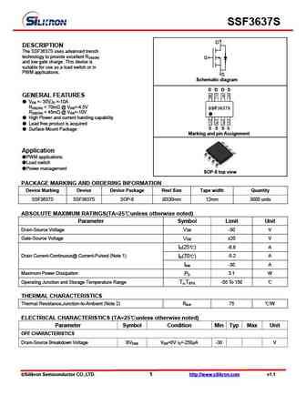
SSF3637S D DESCRIPTION The SSF3637S uses advanced trench technology to provide excellent RDS(ON) G and low gate charge .This device is suitable for use as a load switch or in PWM applications. S Schematic diagram GENERAL FEATURES VDS =- 30V,ID =-10A R
9.8. Size:496K silikron
ssf3610.pdf 
SSF3610 D DESCRIPTION The SSF3610 uses advanced trench technology to provide excellent RDS(ON) G and low gate charge .This device is suitable for use as a load switch or in PWM applications. S Schematic diagram GENERAL FEATURES VDS = 30V,ID =11A RDS(ON)
9.9. Size:457K silikron
ssf3620.pdf 
SSF3620 DESCRIPTION The SSF3620 uses advanced trench technology to provide excellent RDS(ON) and low gate charge .This device is suitable for use as a load switch or in PWM applications. Schematic diagram GENERAL FEATURES VDS = 30V,ID =7A RDS(ON)
9.10. Size:394K silikron
ssf3604.pdf 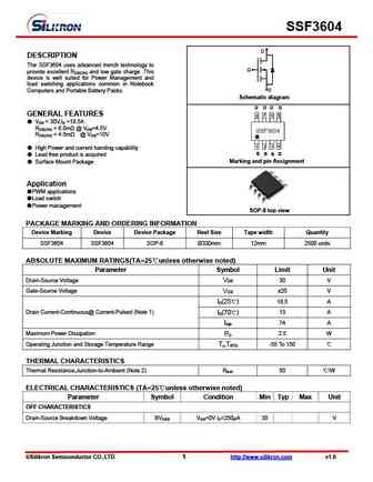
SSF3604 D DESCRIPTION The SSF3604 uses advanced trench technology to G provide excellent RDS(ON) and low gate charge .This device is well suited for Power Management and load switching applications common in Notebook Computers and Portable Battery Packs. S Schematic diagram GENERAL FEATURES VDS = 30V,ID =18.5A RDS(ON)
9.11. Size:323K silikron
ssf3626.pdf 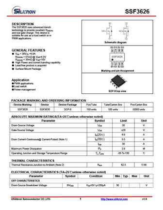
SSF3626 DESCRIPTION The SSF3626 uses advanced trench technology to provide excellent R DS(ON) and low gate charge .This device is suitable for use as a load switch or in PWM applications. Schematic diagram GENERAL FEATURES VDS = 30V,ID =6.9A R
9.12. Size:503K silikron
ssf3637.pdf 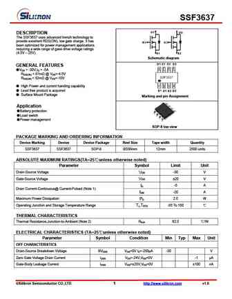
SSF3637 D1 D2 DESCRIPTION The SSF3637 uses advanced trench technology to provide excellent RDS(ON), low gate charge. It has G1 G2 been optimized for power management applications requiring a wide range of gave drive voltage ratings (4.5V 25V). S1 S2 Schematic diagram GENERAL FEATURES VDS = -30V,ID = -5A RDS(ON)
9.13. Size:421K silikron
ssf3615.pdf 
SSF3615 D DESCRIPTION The SSF3615 uses advanced trench technology to provide excellent RDS(ON) G and low gate charge .This device is suitable for use as a load switch or in PWM applications. S Schematic diagram GENERAL FEATURES VDS =- 30V,ID =-10A RDS(ON)
9.14. Size:339K silikron
ssf3639c.pdf 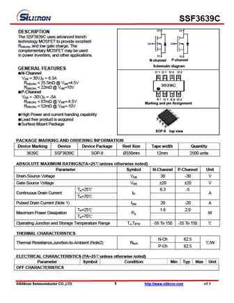
SSF3639C DESCRIPTION The SSF3639C uses advanced trench technology MOSFET to provide excellent RDS(ON) and low gate charge. The complementary MOSFET may be used in power inverters, and other applications. P-channel N-channel Schematic diagram GENERAL FEATURES N-Channel VDS = 30V,ID = 6.3A RDS(ON)
9.15. Size:578K silikron
ssf3610e.pdf 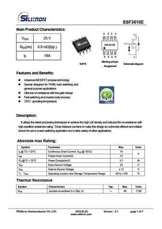
SSF3610E Main Product Characteristics VDSS 25 V SSF3610E SSF3610E RDS(on) 6.8 m (typ.) ID 18A Marking and pin Sc hemat ic d ia gr am SOP-8 A s sign ment Features and Benefits Advanced MOSFET process technology Special designed for PWM, load switching and general purpose applications Ultra low on-resistance with low gate charge Fast switching an
9.16. Size:324K silikron
ssf3611e.pdf 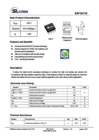
SSF3611E Main Product Characteristics VDSS -30 V RDS(on) 10.6 m (typ.) ID -12A Marking and pin SOP-8 Schematic diagram Assignment Features and Benefits Advanced trench MOSFET process technology Special designed for PWM, load switching and general purpose applications Ultra low on-resistance with low gate charge Fast switching and reverse body recovery
9.17. Size:453K goodark
ssf3612e.pdf 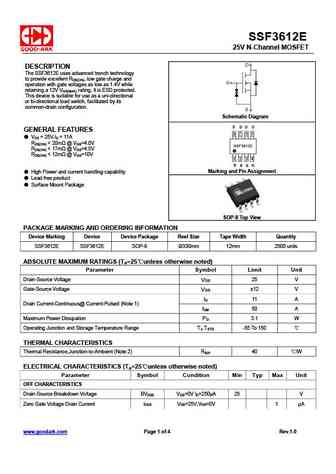
SSF3612E 25V N-Channel MOSFET DESCRIPTION The SSF3612E uses advanced trench technology to provide excellent RDS(ON), low gate charge and operation with gate voltages as low as 1.4V while retaining a 12V VGS(MAX) rating. It is ESD protected. This device is suitable for use as a uni-directional or bi-directional load switch, facilitated by its common-drain configuration. Schem
Другие IGBT... SSF3616, SSF3617, SSF3620, SSF3624, SSF3626, SSF3637, SSF3637S, SSF3639C, IRF3205, SSF3745, SSF3904A, SSF3944J7-HF, SSF3960J7-HF, SSF3N80D, SSF3N80F, SSF4004, SSF4004S
