APM4048DU4. Аналоги и основные параметры
Наименование производителя: APM4048DU4
Тип транзистора: MOSFET
Полярность: NP
Предельные значения
Pd ⓘ
- Максимальная рассеиваемая мощность: 25 W
|Vds|ⓘ - Максимально допустимое напряжение сток-исток: 40 V
|Vgs|ⓘ - Максимально допустимое напряжение затвор-исток: 20 V
|Id| ⓘ - Максимально допустимый постоянный ток стока: 7.5(6) A
Tj ⓘ - Максимальная температура канала: 150 °C
Электрические характеристики
RDSonⓘ - Сопротивление сток-исток открытого транзистора: 0.033(0.048) Ohm
Тип корпуса: TO252-4
Аналог (замена) для APM4048DU4
- подборⓘ MOSFET транзистора по параметрам
APM4048DU4 даташит
..1. Size:484K anpec
apm4048du4.pdf 
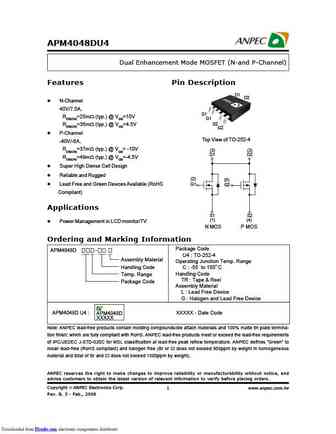
APM4048DU4 Dual Enhancement Mode MOSFET (N-and P-Channel) Features Pin Description D1 D2 N-Channel 40V/7.5A, S1 RDS(ON)=25m (typ.) @ VGS=10V G1 S2 RDS(ON)=35m (typ.) @ VGS=4.5V G2 P-Channel Top View of TO-252-4 -40V/-6A, RDS(ON)=37m (typ.) @ VGS= -10V (3) (3) D1 D2 RDS(ON)=49m (typ.) @ VGS=-4.5V Super High Dense Cell Design Reliable and Rugged (2) (5) G
7.1. Size:255K anpec
apm4048adu4.pdf 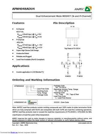
APM4048ADU4 Dual Enhancement Mode MOSFET (N-and P-Channel) Features Pin Description D1 D2 N-Channel 40V/7.5A, RDS(ON)=25m (typ.) @ VGS=10V RDS(ON)=35m (typ.) @ VGS=4.5V P-Channel -40V/-6A, RDS(ON)=37m (typ.) @ VGS= -10V S1 G1 S2 G2 RDS(ON)=49m (typ.) @ VGS=-4.5V Top View of TO-252-4 Super High Dense Cell Design Avalanche Rated (3) (3) D1 D2 Reliable and Rugge
9.1. Size:202K anpec
apm4050pu.pdf 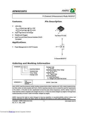
APM4050PU P-Channel Enhancement Mode MOSFET Features Pin Description -40V/-25A, RDS(ON)=33m (typ.) @ VGS=-10V G D RDS(ON)=47m (typ.) @ VGS=-4.5V Super High Dense Cell Design S Reliable and Rugged Top View of TO-252 Lead Free and Green Devices Available (RoHS S Compliant) Applications G Power Management in LCD/TV Inverter D P-Channel MOSFET Ordering and Mar
9.2. Size:206K anpec
apm4018nu.pdf 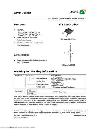
APM4018NU N-Channel Enhancement Mode MOSFET Features Pin Description 40V/60A, D RDS(ON)=6.5m (typ.) @ VGS=10V G RDS(ON)=9.5m (typ.) @ VGS=4.5V S Super High Dense Cell Design Top View of TO-252-3 Reliable and Rugged Lead Free and Green Devices Available D (RoHS Compliant) G Applications Power Management in Desktop Computer or S DC/DC Converters N-Channel MOSFET O
9.3. Size:200K anpec
apm4010nu.pdf 
APM4010NU N-Channel Enhancement Mode MOSFET Features Pin Description 40V/57A, RDS(ON)=8.2m (typ.) @ VGS=10V G D RDS(ON)=13m (typ.) @ VGS=5V S Super High Dense Cell Design Reliable and Rugged Top View of TO-252 Lead Free and Green Devices Available (RoHS D Compliant) Applications G Power Management in LCD monitor/TV inverter. S N-Channel MOSFET Ordering and Marking
9.4. Size:493K anpec
apm4052du4.pdf 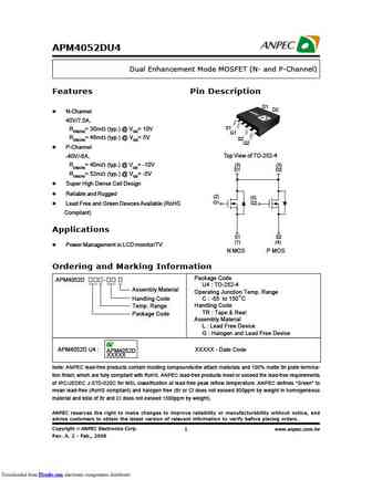
APM4052DU4 Dual Enhancement Mode MOSFET (N- and P-Channel) Features Pin Description D1 D2 N-Channel 40V/7.5A, S1 RDS(ON)= 30m (typ.) @ VGS= 10V G1 RDS(ON)= 46m (typ.) @ VGS= 5V S2 G2 P-Channel Top View of TO-252-4 -40V/-6A, RDS(ON)= 40m (typ.) @ VGS= -10V (3) (3) D1 D2 RDS(ON)= 52m (typ.) @ VGS= -5V Super High Dense Cell Design Reliable and Rugged (2) (5)
9.5. Size:202K anpec
apm4030nu.pdf 
APM4030NU N-Channel Enhancement Mode MOSFET Features Pin Description 40V/35A, RDS(ON)=17m (typ.) @ VGS=10V RDS(ON)=26m (typ.) @ VGS=4.5V G D Super High Dense Cell Design S Top View of TO-252 Reliable and Rugged Lead Free and Green Devices Available (RoHS (2) D1 Compliant) Applications (1) G1 Inverter Application in LCM and LCD TV S1 (3) N-Channel MOSFET Order
9.6. Size:201K anpec
apm4030anu.pdf 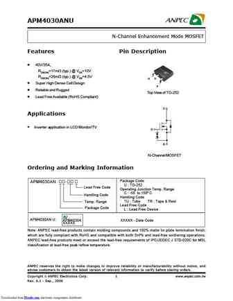
APM4030ANU N-Channel Enhancement Mode MOSFET Features Pin Description 40V/35A, RDS(ON)=17m (typ.) @ VGS=10V RDS(ON)=26m (typ.) @ VGS=4.5V G D Super High Dense Cell Design S Reliable and Rugged Top View of TO-252 Lead Free Available (RoHS Compliant) D Applications Inverter application in LCD Monitor/TV G S N-Channel MOSFET Ordering and Marking Information Packag
9.7. Size:202K anpec
apm4012nu.pdf 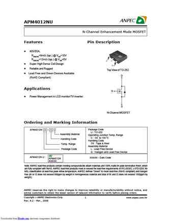
APM4012NU N-Channel Enhancement Mode MOSFET Features Pin Description 40V/55A, RDS(ON)=9m (typ.) @ VGS=10V RDS(ON)=12m (typ.) @ VGS=5V Super High Dense Cell Design Reliable and Rugged Top View of TO-252 Lead Free and Green Devices Available D (RoHS Compliant) Applications G Power Management in LCD monitor/TV inverter. S N-Channel MOSFET Ordering and Marking Informati
9.8. Size:231K anpec
apm4008nu.pdf 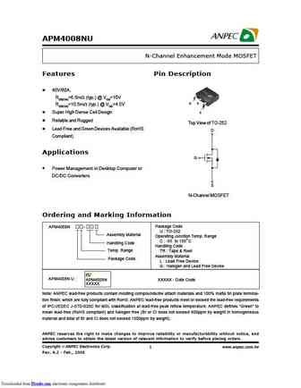
APM4008NU N-Channel Enhancement Mode MOSFET Features Pin Description 40V/60A, RDS(ON)=6.5m (typ.) @ VGS=10V G D RDS(ON)=10.5m (typ.) @ VGS=4.5V S Super High Dense Cell Design Reliable and Rugged Top View of TO-252 Lead Free and Green Devices Available (RoHS D Compliant) Applications G Power Management in Desktop Computer or DC/DC Converters S N-Channel MOSFET
9.9. Size:197K anpec
apm4017pu.pdf 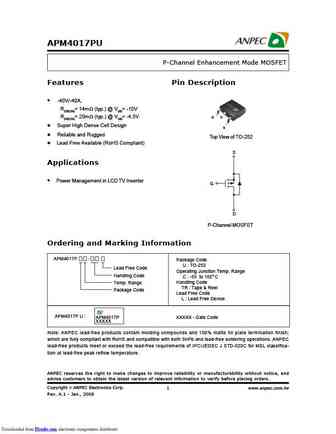
APM4017PU P-Channel Enhancement Mode MOSFET Features Pin Description -40V/-40A, RDS(ON)= 14m (typ.) @ VGS= -10V G D RDS(ON)= 20m (typ.) @ VGS= -4.5V Super High Dense Cell Design S Reliable and Rugged Top View of TO-252 Lead Free Available (RoHS Compliant) S Applications Power Management in LCD TV Inverter G D P-Channel MOSFET Ordering and Marking Informatio
9.10. Size:201K anpec
apm4015pu.pdf 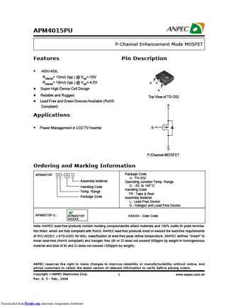
APM4015PU P-Channel Enhancement Mode MOSFET Features Pin Description -40V/-45A, RDS(ON)= 13m (typ.) @ VGS=-10V G D RDS(ON)= 19m (typ.) @ VGS=-4.5V Super High Dense Cell Design S Reliable and Rugged Top View of TO-252 Lead Free and Green Devices Available (RoHS S Compliant) Applications G Power Management in LCD TV Inverter D P-Channel MOSFET Ordering and M
9.11. Size:196K anpec
apm4034nu.pdf 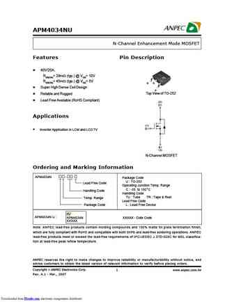
APM4034NU N-Channel Enhancement Mode MOSFET Features Pin Description 40V/20A, RDS(ON)= 29m (typ.) @ VGS= 10V RDS(ON)= 45m (typ.) @ VGS= 5V G D Super High Dense Cell Design S Top View of TO-252 Reliable and Rugged Lead Free Available (RoHS Compliant) (2) D1 Applications (1) G1 Inventer Application in LCM and LCD TV S1 (3) N-Channel MOSFET Ordering and Marking
9.12. Size:201K anpec
apm4050apu.pdf 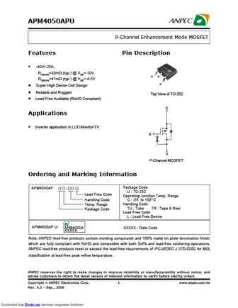
APM4050APU P-Channel Enhancement Mode MOSFET Features Pin Description -40V/-25A, RDS(ON)=33m (typ.) @ VGS=-10V G D RDS(ON)=47m (typ.) @ VGS=-4.5V S Super High Dense Cell Design Reliable and Rugged Top View of TO-252 Lead Free Available (RoHS Compliant) S Applications Inverter application in LCD Monitor/TV G D P-Channel MOSFET Ordering and Marking Informatio
9.13. Size:229K anpec
apm4008ng.pdf 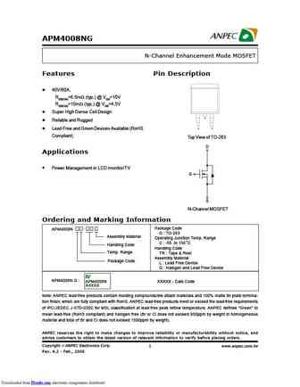
APM4008NG N-Channel Enhancement Mode MOSFET Features Pin Description 40V/60A, RDS(ON)=6.5m (typ.) @ VGS=10V RDS(ON)=10m (typ.) @ VGS=4.5V Super High Dense Cell Design D Reliable and Rugged Lead Free and Green Devices Available (RoHS G S Compliant) Top View of TO-263 D Applications Power Management in LCD monitor/TV G S N-Channel MOSFET Ordering and Marking Infor
9.14. Size:195K anpec
apm4053pu.pdf 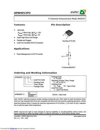
APM4053PU P-Channel Enhancement Mode MOSFET Features Pin Description -40V/-25A, RDS(ON)= 40m (typ.) @ VGS= -10V G D RDS(ON)= 55m (typ.) @ VGS= -5V Super High Dense Cell Design S Reliable and Rugged Top View of TO-252 Lead Free Available (RoHS Compliant) S Applications Power Management in LCD TV Inverter G D P-Channel MOSFET Ordering and Marking Information
9.15. Size:229K anpec
apm4015k.pdf 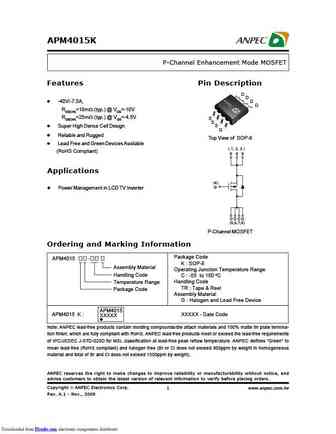
APM4015K P-Channel Enhancement Mode MOSFET Features Pin Description D D -40V/-7.5A, D D RDS(ON)=18m (typ.) @ VGS=-10V RDS(ON)=25m (typ.) @ VGS=-4.5V S S S Super High Dense Cell Design G Reliable and Rugged Top View of SOP-8 Lead Free and Green Devices Available ( 1, 2, 3 ) (RoHS Compliant) S S S Applications (4) G Power Management in LCD TV Inverter D D D D
9.16. Size:514K sino
apm4030bnu.pdf 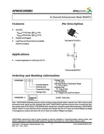
APM4030BNU N-Channel Enhancement Mode MOSFET Features Pin Description 40V/35A, D RDS(ON)=17m (typ.) @ VGS=10V S RDS(ON)=26m (typ.) @ VGS=4.5V G Reliable and Rugged Top View of TO-252-3 Lead Free and Green Devices Available (RoHS Compliant) (2) D1 (1) Applications G1 Inverter Application in LCM and LCD TV. S1 (3) N-Channel MOSFET Ordering and Marking Informati
9.17. Size:515K sino
apm4050bpu.pdf 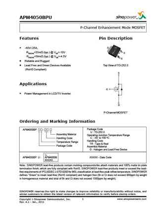
APM4050BPU P-Channel Enhancement Mode MOSFET Features Pin Description D -40V/-25A, RDS(ON)=33m (typ.) @ VGS=-10V S RDS(ON)=59m (typ.) @ VGS=-4.5V G Reliable and Rugged Lead Free and Green Devices Available Top View of TO-252-3 (RoHS Compliant) S Applications G Power Management in LCD/TV Inverter. D P-Channel MOSFET Ordering and Marking Information Package
9.18. Size:1433K kexin
apm4015pu.pdf 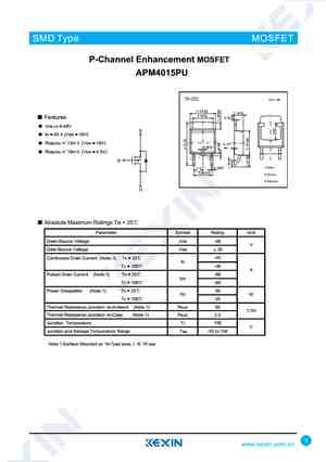
SMD Type MOSFET P-Channel Enhancement MOSFET APM4015PU Typical Characterisitics Drain Current Power Dissipation 60 50 50 40 40 30 30 20 20 10 10 TC=25oC,VG=-10V TC=25oC 0 0 0 20 40 60 80 100 120 140 160 180 0 20 40 60 80 100 120 140 160 Tj - Junction Temperature ( C) Tj - Junction Temperature ( C) Safe Operation Area Thermal Transient Impedance 2 200 Duty = 0.
9.19. Size:1539K cn vbsemi
apm4050puc.pdf 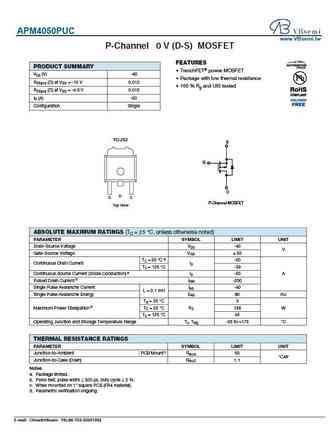
APM4050PUC www.VBsemi.tw P-Channel 4 0 V (D-S) MOSFET FEATURES PRODUCT SUMMARY TrenchFET power MOSFET VDS (V) -40 Package with low thermal resistance RDS(on) ( ) at VGS = -10 V 0.012 100 % Rg and UIS tested RDS(on) ( ) at VGS = -4.5 V 0.015 ID (A) -50 Configuration Single TO-252 S G D D G S P-Channel MOSFET Top View ABSOLUTE MAXIMUM RATINGS (TC = 25 C, u
9.20. Size:1483K cn vbsemi
apm4010nuc.pdf 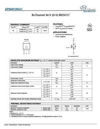
APM4010NUC www.VBsemi.tw N-Channel 40-V (D-S) MOSFET FEATURES PRODUCT SUMMARY TrenchFET Power MOSFET VDS (V) RDS(on) ( ) ID (A)a, c Qg (Typ.) 100 % Rg and UIS Tested RoHS 0.0050 at VGS = 10 V 85 COMPLIANT 40 80 nC 0.0065 at VGS = 4.5 V 70 APPLICATIONS Synchronous Rectification Power Supplies D TO-252 G G D S S N-Channel MOSFET ABSOLUTE MAXIMUM R
9.21. Size:1543K cn vbsemi
apm4050apuc.pdf 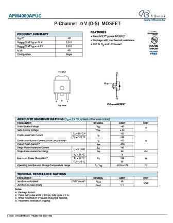
APM4050APUC www.VBsemi.tw P-Channel 4 0 V (D-S) MOSFET FEATURES PRODUCT SUMMARY TrenchFET power MOSFET VDS (V) -40 Package with low thermal resistance RDS(on) ( ) at VGS = -10 V 0.012 100 % Rg and UIS tested RDS(on) ( ) at VGS = -4.5 V 0.015 ID (A) -50 Configuration Single TO-252 S G D D G S P-Channel MOSFET Top View ABSOLUTE MAXIMUM RATINGS (TC = 25 C,
Другие MOSFET... APM4015K
, APM4015PU
, APM4017PU
, APM4018NU
, APM4030ANU
, APM4030NU
, APM4034NU
, APM4048ADU4
, IRFZ24N
, APM4050APU
, APM4050PU
, APM4052DU4
, APM4053PU
, APM4101K
, APM4115PU
, APM4210K
, APM4220
.
History: BRCS26N50PA
