4812. Аналоги и основные параметры
Наименование производителя: 4812
Тип транзистора: MOSFET
Полярность: N
Предельные значения
Pd ⓘ
- Максимальная рассеиваемая мощность: 2 W
|Vds|ⓘ - Максимально допустимое напряжение сток-исток: 30 V
|Vgs|ⓘ - Максимально допустимое напряжение затвор-исток: 20 V
|Id| ⓘ - Максимально допустимый постоянный ток стока: 6.9 A
Tj ⓘ - Максимальная температура канала: 150 °C
Электрические характеристики
RDSonⓘ - Сопротивление сток-исток открытого транзистора: 0.028 Ohm
Тип корпуса: SOP8
- подборⓘ MOSFET транзистора по параметрам
4812 даташит
..1. Size:687K shenzhen
4812.pdf 

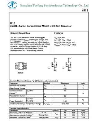
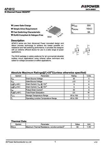
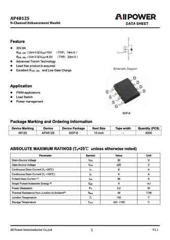
Shenzhen Tuofeng Semiconductor Technology Co., Ltd 4812 4812 Dual N-Channel Enhancement Mode Field Effect Transistor General Description Features The 4812 uses advanced trench technology to VDS (V) = 30V provide excellent RDS(ON) and low gate charge. The ID = 8.0A (VGS = 10V) two MOSFETs make a compact and efficient switch RDS(ON)
0.1. Size:64K vishay
si4812dy.pdf 

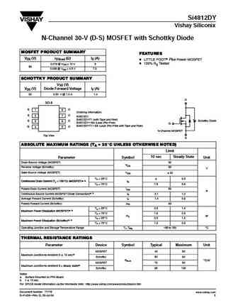
Si4812DY Vishay Siliconix N-Channel 30-V (D-S) MOSFET with Schottky Diode MOSFET PRODUCT SUMMARY FEATURES VDS (V) rDS(on) (W) ID (A) D LITTLE FOOTr Plus Power MOSFET D 100% Rg Tested 0.018 @ VGS = 10 V 9 30 30 0.028 @ VGS = 4.5 V 7.3 SCHOTTKY PRODUCT SUMMARY VSD (V) VDS (V) Diode Forward Voltage IF (A) 30 0.50 V @ 1.0 A 1.4 D SO-8 SD 1 8 Ordering Information S D 2 7 Si4
0.2. Size:249K vishay
si4812bdy.pdf 

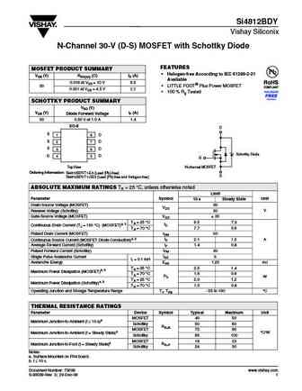
Si4812BDY Vishay Siliconix N-Channel 30-V (D-S) MOSFET with Schottky Diode FEATURES MOSFET PRODUCT SUMMARY Halogen-free According to IEC 61249-2-21 VDS (V) RDS(on) ( )ID (A) Available 0.016 at VGS = 10 V 9.5 30 LITTLE FOOT Plus Power MOSFET 0.021 at VGS = 4.5 V 7.7 100 % Rg Tested SCHOTTKY PRODUCT SUMMARY VSD (V) VDS (V) IF (A) Diode Forward Voltage 30 0.
0.3. Size:154K diodes
dmg4812sss.pdf 

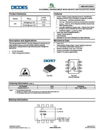
DMG4812SSS N-CHANNEL ENHANCEMENT MODE MOSFET WITH SCHOTTKY DIODE Product Summary Features DIOFET utilizes a unique patented process to monolithically ID max integrate a MOSFET and a Schottky in a single die to deliver V(BR)DSS RDS(on) TA = 25 C Low RDS(ON) - minimizes conduction losses Low VSD - reducing the losses due to body diode conduction 15m @ VGS= 10V 10
0.4. Size:147K utc
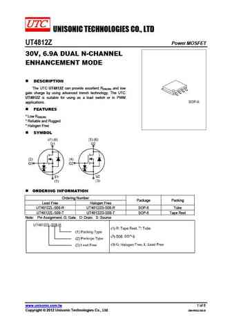
ut4812z.pdf 

UNISONIC TECHNOLOGIES CO., LTD UT4812Z Power MOSFET 30V, 6.9A DUAL N-CHANNEL ENHANCEMENT MODE DESCRIPTION The UTC UT4812Z can provide excellent RDS(ON) and low gate charge by using advanced trench technology. The UTC UT4812Z is suitable for using as a load switch or in PWM applications. FEATURES * Low RDS(ON) * Reliable and Rugged * Halogen Free SYMBOL ORDERIN
0.5. Size:252K utc
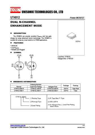
ut4812.pdf 

UNISONIC TECHNOLOGIES CO., LTD UT4812 Power MOSFET DUAL N-CHANNEL ENHANCEMENT MODE DESCRIPTION The UT4812 can provide excellent RDS(ON) and low gate charge by using advanced trench technology. The UT4812 is suitable for using as a load switch or in PWM applications. FEATURES * 30V/6.9A * Low RDS(ON) * Reliable and Rugged SYMBOL (7) (8) (5) (6) Lead-free UT481
0.6. Size:485K willas
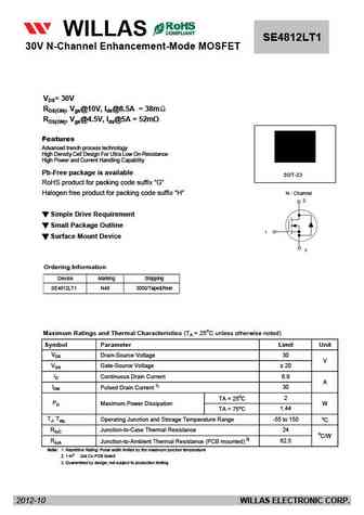
se4812lt1.pdf 

FM120-M WILLAS THRU SE4812LT1 30V N-Channel Enhancement-Mode MOSFET FM1200-M 1.0A SURFACE MOUNT SCHOTTKY BARRIER RECTIFIERS -20V- 200V SOD-123 PACKAGE Pb Free Product Package outline Features Batch process design, excellent power dissipation offers better reverse leakage current and thermal resistance. SOD-123H Low profile surface mounted application in order to V
0.7. Size:255K aosemi
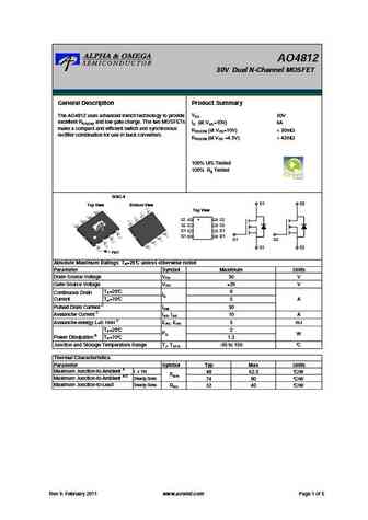
ao4812.pdf 

AO4812 30V Dual N-Channel MOSFET General Description Product Summary VDS 30V The AO4812 uses advanced trench technology to provide excellent RDS(ON) and low gate charge. The two MOSFETs ID (at VGS=10V) 6A make a compact and efficient switch and synchronous RDS(ON) (at VGS=10V)
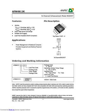
0.8. Size:202K anpec
apm4812k.pdf 

APM4812K N-Channel Enhancement Mode MOSFET Features Pin Description 30V/8A, RDS(ON)= 18m (typ.) @ VGS= 10V RDS(ON)= 26m (typ.) @ VGS= 4.5V Super High Dense Cell Design Reliable and Rugged Lead Free Available (RoHS Compliant) Top View of SOP - 8 D D D D Applications Power Management in Notebook Computer, Portable Equipment and Battery Powered G Systems S S S N-C
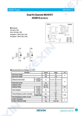
0.9. Size:1097K kexin
ao4812.pdf 

SMD Type MOSFET Dual N-Channel MOSFET AO4812 (KO4812) SOP-8 Unit mm Features VDS (V) = 30V ID = 6A (VGS = 10V) 1.50 0.15 RDS(ON) 30m (VGS = 10V) RDS(ON) 42m (VGS = 4.5V) 1 S2 5 D1 6 D1 2 G2 7 D2 3 S1 8 D2 4 G1 D1 D2 G1 G2 S1 S2 Absolute Maximum Ratings Ta = 25 Parameter Symbol Rating Unit Drain-Source Voltage VDS 30 V Gate-So
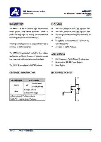
0.10. Size:466K ait semi
am4812.pdf 

AiT Semiconductor Inc. AM4812 www.ait-ic.com 30V N-CHANNEL ENHANCEMENT MODE MOSFET DESCRIPTION FEATURES The AM4812 is the N-Channel logic enhancement 30V / 7.8A, R = 16m (typ.)@V = 10V DS(ON) GS mode power field effect transistor which is 30V / 5.8A, R = 22m (typ.)@V = 4.5V DS(ON) GS produced using high cell density. Advanced trench Super high density cell design f
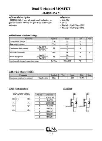
0.11. Size:429K elm
elm34812aa.pdf 

Dual N-channel MOSFET ELM34812AA-N General description Features ELM34812AA-N uses advanced trench technology to Vds=20V provide excellent Rds(on), low gate charge and low gate Id=7A resistance. Rds(on)
0.12. Size:392K elm
elm14812aa.pdf 

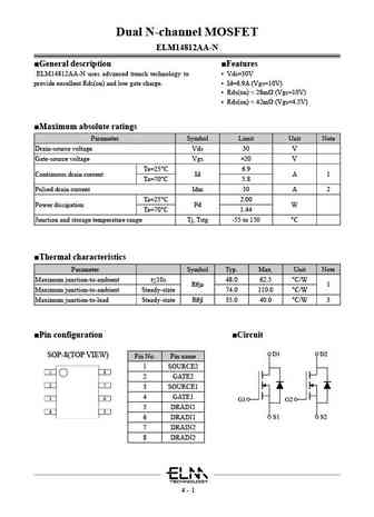
Dual N-channel MOSFET ELM14812AA-N General description Features ELM14812AA-N uses advanced trench technology to Vds=30V provide excellent Rds(on) and low gate charge. Id=6.9A (Vgs=10V) Rds(on)
0.13. Size:1388K semtron
smc4812.pdf 

SMC4812 30V N-Channel Enhancement Mode MOSFET DESCRIPTION FEATURE The SMC4812 is the N-Channel logic 30V / 7.8A, RDS(ON) =14m (typ.)@VGS =10V enhancement mode power field effect transistor is 30V / 5.8A, RDS(ON) =20m (typ.)@VGS =4.5V produced using high cell density. advanced trench Super high density cell design for extremely low technology to provide exce
0.14. Size:282K tiptek
tp4812nr.pdf 

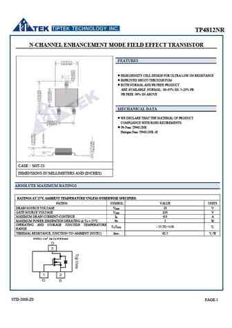
TP4812NR N-CHANNEL ENHANCEMENT MODE FIELD EFFECT TRANSISTOR FEATURES HIGH DENSITY CELL DESIGN FOR ULTRA LOW ON-RESISTANCE IMPROVED SHOOT-THROUGH FOM BOTH NORMAL AND PB FREE PRODUCT ARE AVAILABLE NORMAL 80 95% SN, 5 20% PB PB FREE 99% SN ABOVE MECHANICAL DATA WE DECLARE THAT THE MATERIAL OF PRODUCT COMPLIANCE WITH ROHS REUIREMENTS. Pb Free TP4812NR
0.17. Size:640K eternal
es4812.pdf 

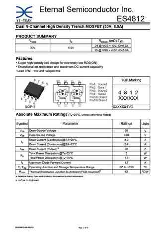
Eternal Semiconductor Inc. ES4812 Dual N-Channel High Density Trench MOSFET (30V, 6.9A) PRODUCT SUMMARY VDSS ID RDS(on) (m ) Typ. 24 @ VGS = 10V, ID=6.9A 30V 6.9A 30 @ VGS = 4.5V, ID=5.8A Features Super high density cell design for extremely low RDS(ON) Exceptional on-resistance and maximum DC current capability Lead Pb -free and halogen-free TOP Marking 4 8 1 2
0.18. Size:1405K msksemi
ao4812-ms.pdf 

www.msksemi.com AO4812-MS Semiconductor Compiance D1 Product D1 D2 Summary D2 30V VDS I (at V =10V) 6A D GS S1 G1 R (at V =10V)
0.19. Size:1599K winsok
wsp4812.pdf 

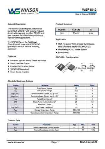
WSP4812 Dual N-Channel MOSFET General Description Product Summery The WSP4812 is the highest performance BVDSS RDSON ID trench N-ch MOSFET with extreme high cell density,which provide excellent RDSON and 20m 30V 8.0A gate chargens for most of the synchronous buck converter applications . Application The WSP4812 meet the RoHS and High Frequency Point-of-Load Synchronou
0.20. Size:769K cn sps
sm4812prl.pdf 

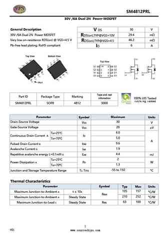
SM4812PRL 30V /6A Dual 2N Power MOSFET C B03C B 30V /6A Dual 2N Power MOSFET 6B03C General Description 30 V V DS 30V /6A Dual 2N Power MOSFET 29.4 m RDS(on),TYP@VGS=10V Very low on-resistance RDS(on) @ VGS=4.5 V 46.2 m RDS(on),TYP@VGS=4.5 Pb-free lead plating; RoHS compliant 6 A ID Tape and reel Part ID Package Type Marking infomation 100% UIS Tested 100% Rg Tested SM4812PR
0.21. Size:851K cn vbsemi
ao4812.pdf 

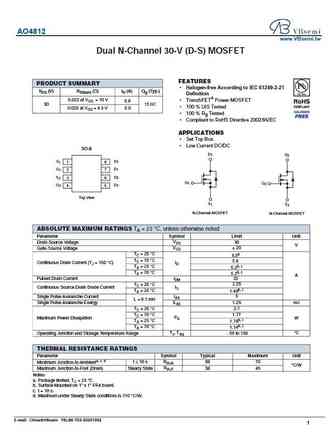
AO4812 www.VBsemi.tw Dual N-Channel 30-V (D-S) MOSFET FEATURES PRODUCT SUMMARY Halogen-free According to IEC 61249-2-21 VDS (V) RDS(on) ( )ID (A) Qg (Typ.) Definition 0.022 at VGS = 10 V TrenchFET Power MOSFET 6.8 30 15 nC 100 % UIS Tested 0.026 at VGS = 4.5 V 6.0 100 % Rg Tested Compliant to RoHS Directive 2002/95/EC APPLICATIONS Set Top Box L
0.22. Size:511K cn hmsemi
hm4812.pdf 

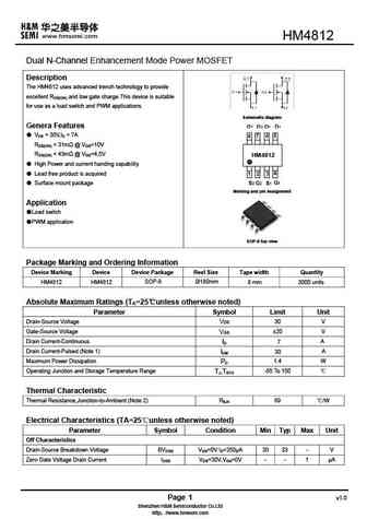
HM4812 Dual N-Channel Enhancement Mode Power MOSFET Description The HM4812 uses advanced trench technology to provide excellent RDS(ON) and low gate charge.This device is suitable for use as a load switch and PWM applications. Schematic diagram Genera Features VDS = 30V,ID = 7A RDS(ON)
Другие MOSFET... 4501
, 4542
, 4606
, 4611
, 4612
, 4616
, 4622
, 4803
, SPP20N60C3
, 4835
, 4920
, 4946
, 4953
, 6604
, 8810
, 8820
, 8822
.
History: 9926A
