4920. Аналоги и основные параметры
Наименование производителя: 4920
Тип транзистора: MOSFET
Полярность: N
Предельные значения
Pd ⓘ
- Максимальная рассеиваемая мощность: 2 W
|Vds|ⓘ - Максимально допустимое напряжение сток-исток: 25 V
|Vgs|ⓘ - Максимально допустимое напряжение затвор-исток: 20 V
|Id| ⓘ - Максимально допустимый постоянный ток стока: 7 A
Tj ⓘ - Максимальная температура канала: 150 °C
Электрические характеристики
RDSonⓘ - Сопротивление сток-исток открытого транзистора: 0.025 Ohm
Тип корпуса: SOP8
- подборⓘ MOSFET транзистора по параметрам
4920 даташит
..1. Size:862K shenzhen
4920.pdf 

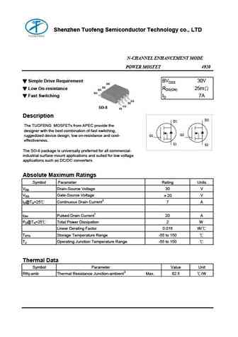
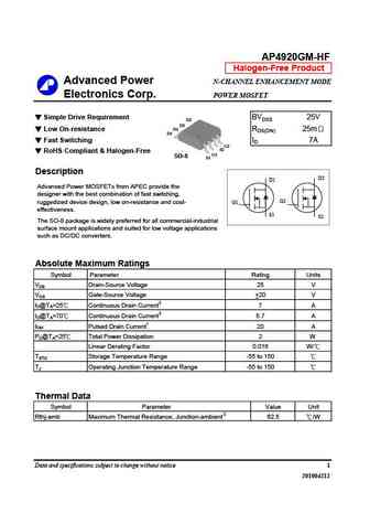
Shenzhen Tuofeng Semiconductor Technology co., LTD N-CHANNEL ENHANCEMENT MODE POWER MOSFET 4920 Simple Drive Requirement BVDSS 30V D2 D2 Low On-resistance RDS(ON) 25m D1 D1 Fast Switching ID 7A G2 S2 G1 SO-8 S1 Description D2 D1 The TUOFENG MOSFETs from APEC provide the designer with the best combination of fast s
0.1. Size:254K motorola
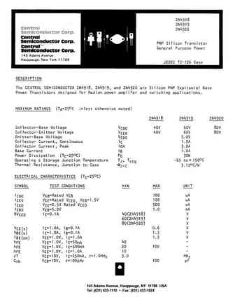
2n4918 2n4919 2n4920.pdf 

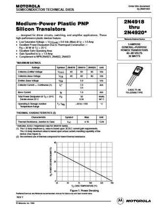
Order this document MOTOROLA by 2N4918/D SEMICONDUCTOR TECHNICAL DATA 2N4918 Medium-Power Plastic PNP thru Silicon Transistors * 2N4920 . . . designed for driver circuits, switching, and amplifier applications. These high performance plastic devices feature *Motorola Preferred Device Low Saturation Voltage VCE(sat) = 0.6 Vdc (Max) @ IC = 1.0 Amp 3 AMPERE Excellent
0.2. Size:60K sanyo
2sc4920.pdf 

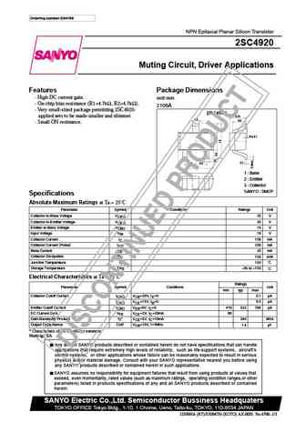
Ordering number EN4766 NPN Epitaxial Planar Silicon Transistor 2SC4920 Muting Circuit, Driver Applications Features Package Dimensions High DC current gain. unit mm On-chip bias resistance (R1=4.7k , R2=4.7k ). 2106A Very small-sized package permitting 2SC4920- [2SC4920] applied sets to be made smaller and slimmer. 0.75 0.3 0.6 Small ON resistance. 0 to 0.1
0.3. Size:251K vishay
sq4920ey.pdf 

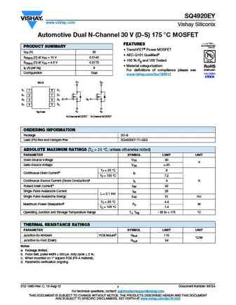
SQ4920EY www.vishay.com Vishay Siliconix Automotive Dual N-Channel 30 V (D-S) 175 C MOSFET FEATURES PRODUCT SUMMARY TrenchFET Power MOSFET VDS (V) 30 AEC-Q101 Qualifiedd RDS(on) ( ) at VGS = 10 V 0.0145 100 % Rg and UIS Tested RDS(on) ( ) at VGS = 4.5 V 0.0175 Material categorization ID (A) per leg 8 For definitions of compliance please see Configuration
0.4. Size:216K vishay
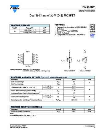
si4920dy.pdf 

Si4920DY Vishay Siliconix Dual N-Channel 30-V (D-S) MOSFET FEATURES PRODUCT SUMMARY Halogen-free According to IEC 61249-2-21 VDS (V) RDS(on) ( )ID (A) Definition 0.025 at VGS = 10 V 6.9 TrenchFET Power MOSFETs 30 0.035 at VGS = 4.5 V 5.8 100 % Rg Tested Compliant to RoHS Directive 2002/95/EC D1 D2 SO-8 S1 1 D1 8 G1 2 D1 7 S2 3 D2 6 G1 G2
0.6. Size:113K onsemi
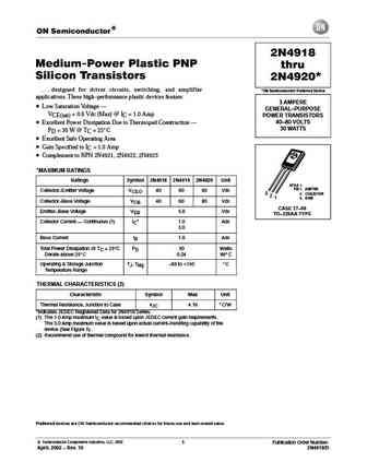
2n4918 2n4919 2n4920.pdf 

ON Semiconductor) 2N4918 Medium-Power Plastic PNP thru Silicon Transistors * 2N4920 . . . designed for driver circuits, switching, and amplifier *ON Semiconductor Preferred Device applications. These high performance plastic devices feature 3 AMPERE Low Saturation Voltage GENERAL PURPOSE VCE(sat) = 0.6 Vdc (Max) @ IC = 1.0 Amp POWER TRANSISTORS 40 80 VOLTS Exc
0.7. Size:117K onsemi
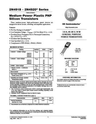
2n4920g9285.pdf 

2N4918 - 2N4920* Series Preferred Device Medium-Power Plastic PNP Silicon Transistors These medium-power, high-performance plastic devices are designed for driver circuits, switching, and amplifier applications. http //onsemi.com Features Pb-Free Package is Available** 3.0 A, 40-80 V, 30 W Low Saturation Voltage - VCE(sat) = 0.6 Vdc (Max) @ IC = 1.0 A Excellent Power Dis
0.8. Size:263K onsemi
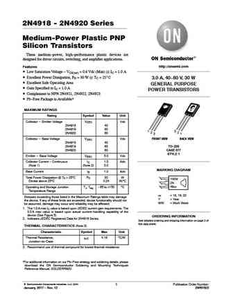
2n4918 2n4919 2n4920 2n4920g.pdf 

2N4918 - 2N4920 Series Medium-Power Plastic PNP Silicon Transistors These medium-power, high-performance plastic devices are designed for driver circuits, switching, and amplifier applications. http //onsemi.com Features Low Saturation Voltage - VCE(sat) = 0.6 Vdc (Max) @ IC = 1.0 A Excellent Power Dissipation, PD = 30 W @ TC = 25_C 3.0 A, 40-80 V, 30 W Excellent Safe Oper
0.9. Size:131K onsemi
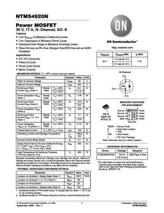
ntms4920n.pdf 

NTMS4920N Power MOSFET 30 V, 17 A, N-Channel, SO-8 Features Low RDS(on) to Minimize Conduction Losses Low Capacitance to Minimize Driver Losses Optimized Gate Charge to Minimize Switching Losses http //onsemi.com These Devices are Pb-Free, Halogen Free/BFR Free and are RoHS Compliant V(BR)DSS RDS(ON) MAX ID MAX Applications DC-DC Converters 4.3 mW @ 10 V 30 V 1
0.10. Size:401K secos
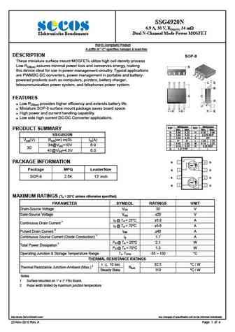
ssg4920n.pdf 

SSG4920N 6.9 A, 30 V, RDS(ON) 34 m Dual N-Channel Mode Power MOSFET Elektronische Bauelemente RoHS Compliant Product A suffix of -C specifies halogen & lead-free DESCRIPTION SOP-8 These miniature surface mount MOSFETs utilize high cell density process Low RDS(on) assures minimal power loss and conserves energy, making B this device ideal for use in power management
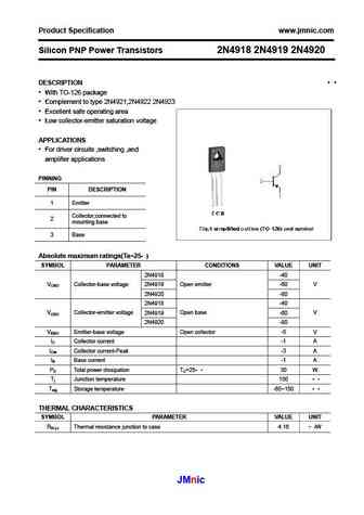
0.11. Size:41K jmnic
2n4918 2n4919 2n4920.pdf 

Product Specification www.jmnic.com Silicon PNP Power Transistors 2N4918 2N4919 2N4920 DESCRIPTION With TO-126 package Complement to type 2N4921,2N4922 2N4923 Excellent safe operating area Low collector-emitter saturation voltage APPLICATIONS For driver circuits ,switching ,and amplifier applications PINNING PIN DESCRIPTION 1 Emitter Collector;connected to
0.12. Size:103K ape
ap4920gm-hf.pdf 

AP4920GM-HF Halogen-Free Product Advanced Power N-CHANNEL ENHANCEMENT MODE Electronics Corp. POWER MOSFET Simple Drive Requirement BVDSS 25V D2 D2 D1 Low On-resistance RDS(ON) 25m D1 Fast Switching ID 7A G2 S2 RoHS Compliant & Halogen-Free G1 SO-8 S1 Description D2 D1 Advanced Power MOSFETs from APEC provide the designer with the best combination of fast s
0.13. Size:336K analog power
am4920n.pdf 

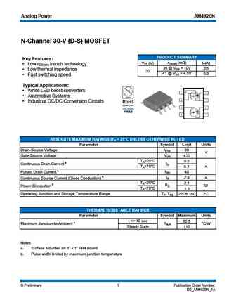
Analog Power AM4920N N-Channel 30-V (D-S) MOSFET PRODUCT SUMMARY Key Features rDS(on) (m ) VDS (V) ID(A) Low r trench technology DS(on) 34 @ VGS = 10V 6.5 Low thermal impedance 30 41 @ VGS = 4.5V 5.9 Fast switching speed Typical Applications White LED boost converters Automotive Systems Industrial DC/DC Conversion Circuits ABSOLUTE MAXIMUM R
0.14. Size:50K kexin
ki4920dy.pdf 

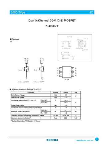
SMD Type IC SMD Type IC Dual N-Channel 30-V (D-S) MOSFET KI4920DY Features Absolute Maximum Ratings Ta = 25 Parameter Symbol Rating Unit Drain-Source Voltage VDS 30 V Gate-Source Voltage VGS 20 Continuous Drain Current (TJ = 150 )* TA =25 ID 6.9 A TA =70 5.5 Pulsed Drain Current IDM 40 Continuous Source Current (Diode Conduction) * IS 1.7 A TA =25 2 Maximum Power Dissipation * P
0.15. Size:620K ait semi
am4920.pdf 

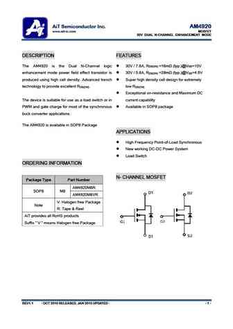
AiT Semiconductor Inc. AM4920 www.ait-ic.com MOSFET 30V DUAL N-CHANNEL ENHANCEMENT MODE DESCRIPTION FEATURES The AM4920 is the Dual N-Channel logic 30V / 7.8A, R =16m (typ.)@V =10V DS(ON) GS enhancement mode power field effect transistor is 30V / 5.8A, R =28m (typ.)@V =4.5V DS(ON) GS produced using high cell density. Advanced trench Super high density cell design f
0.16. Size:892K matsuki electric
me4920 me4920-g.pdf 

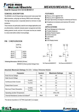
ME4920/ME4920-G Dual N-Channel 30-V (D-S) MOSFET GENERAL DESCRIPTION FEATURES RDS(ON) 35 m @VGS=10V The ME4920 is the N-Channel logic enhancement mode power field RDS(ON) 45 m @VGS=4.5V effect transistors, using high cell density, DMOS trench technology. Super high density cell design for extremely low RDS(ON) This high density process is especially tailored to
0.17. Size:153K silicon standard
ssm4920m.pdf 
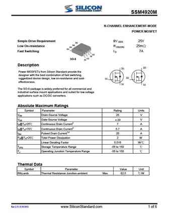
SSM4920M N-CHANNEL ENHANCEMENT-MODE POWER MOSFET Simple Drive Requirement BV 25V DSS D2 D2 Low On-resistance R 25m D1 DS(ON) D1 Fast Switching I 7A D G2 S2 G1 SO-8 S1 Description D2 D1 Power MOSFETs from Silicon Standard provide the designer with the best combination of fast switching, G2 ruggedized device design, low on-resistance and cost- G1 effectiveness. S1 S2
0.18. Size:482K stansontech
stn4920.pdf 

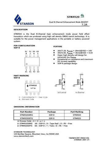
STN4920 Dual N Channel Enhancement Mode MOSFET 7.2A DESCRIPTION STN4920 is the Dual N-Channel logic enhancement mode power field effect transistors which are produced using high cell density DMOS trench technology. It is suitable for the power management applications in the portable or battery powered system. PIN CONFIGURATION FEATURE SOP-8 30V/7.2A, RDS(ON) = 28m @VGS
0.19. Size:909K cn vbsemi
si4920dy-t1.pdf 

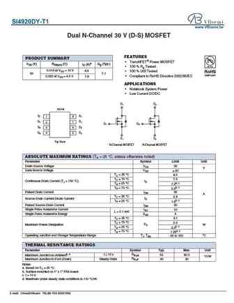
SI4920DY-T1 www.VBsemi.tw Dual N-Channel 30 V (D-S) MOSFET FEATURES PRODUCT SUMMARY TrenchFET Power MOSFET VDS (V) RDS(on) ( ) ID (A)a Qg (Typ.) 100 % Rg Tested 0.016 at VGS = 10 V 8.5 100 % UIS Tested 30 7.1 Compliant to RoHS Directive 2002/95/EC 0.020 at VGS = 4.5 V 7.6 APPLICATIONS Notebook System Power Low Current DC/DC D 1 D 2
0.20. Size:118K inchange semiconductor
2n4918 2n4919 2n4920.pdf 
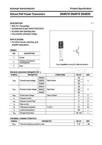
Inchange Semiconductor Product Specification Silicon PNP Power Transistors 2N4918 2N4919 2N4920 DESCRIPTION With TO-126 package Complement to type 2N4921/4922/4923 Excellent safe operating area Low collector saturation voltage APPLICATIONS For driver circuits ,switching ,and amplifier applications PINNING PIN DESCRIPTION 1 Emitter Collector;connected to 2
Другие MOSFET... 4606
, 4611
, 4612
, 4616
, 4622
, 4803
, 4812
, 4835
, K4145
, 4946
, 4953
, 6604
, 8810
, 8820
, 8822
, 9435
, 4953A
.
