1515 datasheet, аналоги, основные параметры
Наименование производителя: 1515 📄📄
Тип транзистора: MOSFET
Полярность: N
Предельные значения
Pd ⓘ - Максимальная рассеиваемая мощность: 460 W
|Vds|ⓘ - Максимально допустимое напряжение сток-исток: 150 V
|Vgs|ⓘ - Максимально допустимое напряжение затвор-исток: 20 V
|Id| ⓘ - Максимально допустимый постоянный ток стока: 150 A
Tj ⓘ - Максимальная температура канала: 175 °C
Электрические характеристики
tr ⓘ - Время нарастания: 110 ns
Cossⓘ - Выходная емкость: 1446 pf
RDSonⓘ - Сопротивление сток-исток открытого транзистора: 0.008 Ohm
Тип корпуса: TO247
📄📄 Копировать
- подборⓘ MOSFET транзистора по параметрам
1515 даташит
..1. Size:1587K goford
1515.pdf 
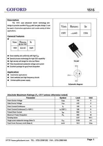
GOFORD 1515 Description The 1515 uses advanced trench technology and design to provide excellent RDS(ON) with low gate charge. It can VDSS RDS(ON) ID be used in Automotive applications and a wide variety of other applications. 150V m 150A
0.1. Size:84K renesas
2sk1515.pdf 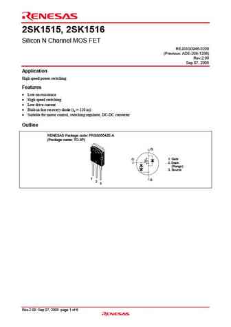
2SK1515, 2SK1516 Silicon N Channel MOS FET REJ03G0946-0200 (Previous ADE-208-1286) Rev.2.00 Sep 07, 2005 Application High speed power switching Features Low on-resistance High speed switching Low drive current Built-in fast recovery diode (trr = 120 ns) Suitable for motor control, switching regulator, DC-DC converter Outline RENESAS Package cod
0.2. Size:119K renesas
r07ds0397ej 2sk115152.pdf 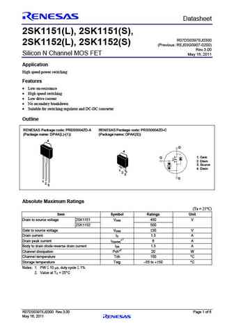
Preliminary Datasheet 2SK1151(L), 2SK1151(S), R07DS0397EJ0300 2SK1152(L), 2SK1152(S) (Previous REJ03G0907-0200) Rev.3.00 Silicon N Channel MOS FET May 16, 2011 Application High speed power switching Features Low on-resistance High speed switching Low drive current No secondary breakdown Suitable for switching regulator and DC-DC converter Outlin
0.3. Size:97K renesas
rej03g0946 2sk1515ds.pdf 
To our customers, Old Company Name in Catalogs and Other Documents On April 1st, 2010, NEC Electronics Corporation merged with Renesas Technology Corporation, and Renesas Electronics Corporation took over all the business of both companies. Therefore, although the old company name remains in this document, it is a valid Renesas Electronics document. We appreciate your understanding.
0.4. Size:173K rohm
2sb1132 2sa1515s 2sb1237.pdf 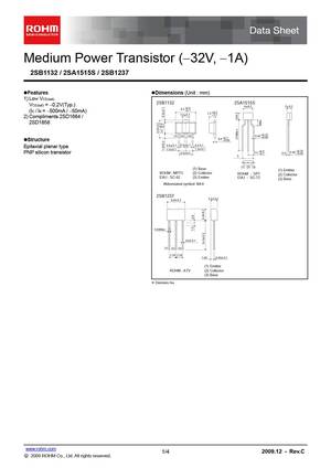
Medium Power Transistor ( 32V, 1A) 2SB1132 / 2SA1515S / 2SB1237 Features Dimensions (Unit mm) 1) Low VCE(sat). 2SB1132 2SA1515S VCE(sat) = 0.2V(Typ.) + + 4 0.2 2 0.2 - - 4.5 +0.2 -0.1 (IC / IB = 500mA / 50mA) 1.5 +0.2 + 1.6 0.1 -0.1 - 2) Compliments 2SD1664 / 2SD1858 (1) (2) (3) 0.45 +0.15 -0.05 0.4 +0.1 Structure -0.05 + + 0.5 0.1 0.
0.5. Size:143K rohm
2sa1515s 2sb1237.pdf 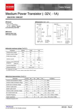
Medium Power Transistor ( 32V, 1A) 2SA1515S / 2SB1237 Features Dimensions (Unit mm) 1) Low VCE(sat). 2SA1515S 2SB1237 + 2.5 0.2 VCE(sat) = 0.2V(Typ.) + + + - 4 0.2 2 0.2 6.8 0.2 - - - (IC / IB = 500mA / 50mA) 2) Compliments 2SD1858 Structure 0.45 +0.15 0.65Max. -0.05 Epitaxial planar type + PNP silicon transistor 0.5 0.1 - 0.45 +0.15 2.5
0.6. Size:28K hitachi
2sc1515.pdf 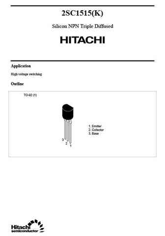
2SC1515(K) Silicon NPN Triple Diffused Application High voltage switching Outline TO-92 (1) 1. Emitter 2. Collector 3. Base 3 2 1 2SC1515 (K) Absolute Maximum Ratings (Ta = 25 C) Item Symbol Ratings Unit Collector to base voltage VCBO 200 V Collector to emitter voltage VCES 200 V VCEO 150 V Emitter to base voltage VEBO 5V Collector current IC 50 mA Collector power dissipat
0.7. Size:110K jiangsu
2sa1515s.pdf 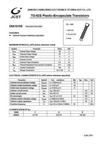
JIANGSU CHANGJIANG ELECTRONICS TECHNOLOGY CO., LTD TO-92S Plastic-Encapsulate Transistors TO 92S 2SA1515S TRANSISTOR (PNP) 1. EMITTER FEATURES 2. COLLECTOR General Purpose Switching Application 3. BASE MAXIMUM RATINGS (Ta=25 unless otherwise noted) Symbol Parameter Value Unit VCBO Collector-Base Voltage -40 V VCEO Collector-Emitter Voltage -32 V VEBO Emitter-
0.8. Size:1008K magnachip
mdu1515urh.pdf 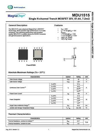
MDU1515 Single N-channel Trench MOSFET 30V, 57.4A, 7.2m General Description Features The MDU1515 uses advanced MagnaChip s MOSFET VDS = 30V Technology, which provides high performance in on-state I = 57.4A @V = 10V D GS resistance, fast switching performance and excellent R DS(ON) quality. MDU1515 is suitable device for DC/DC Converter
0.9. Size:854K ncepower
nce60np1515k.pdf 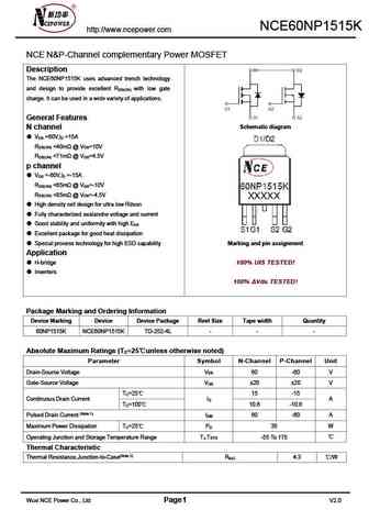
NCE60NP1515K http //www.ncepower.com NCE N&P-Channel complementary Power MOSFET Description The NCE60NP1515K uses advanced trench technology and design to provide excellent R with low gate DS(ON) charge. It can be used in a wide variety of applications. General Features Schematic diagram N channel V =60V,I =15A DS D R
0.10. Size:302K niko-sem
pp1515ad.pdf 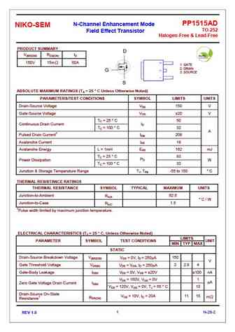
PP1515AD N-Channel Enhancement Mode NIKO-SEM TO-252 Field Effect Transistor Halogen-Free & Lead-Free PRODUCT SUMMARY D V(BR)DSS RDS(ON) ID 150V 15m 50A 1 GATE 2 DRAIN G 3 SOURCE S ABSOLUTE MAXIMUM RATINGS (TA = 25 C Unless Otherwise Noted) PARAMETERS/TEST CONDITIONS SYMBOL LIMITS UNITS Drain-Source Voltage VDS 150 V Gate-Source Voltage VGS 20 V TC
0.11. Size:354K niko-sem
pp1515ak.pdf 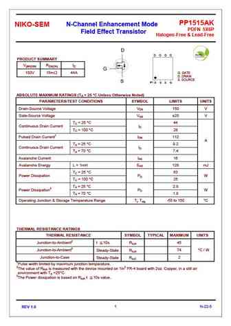
PP1515AK N-Channel Enhancement Mode NIKO-SEM PDFN 5X6P Field Effect Transistor Halogen-Free & Lead-Free D D D D D PRODUCT SUMMARY V(BR)DSS RDS(ON) ID G 150V 15m 44A G. GATE D. DRAIN S. SOURCE S #1 S S S G ABSOLUTE MAXIMUM RATINGS (TA = 25 C Unless Otherwise Noted) PARAMETERS/TEST CONDITIONS SYMBOL LIMITS UNITS Drain-Source Voltage VDS 150 V Gate-Source Vol
0.12. Size:302K niko-sem
pp1515af.pdf 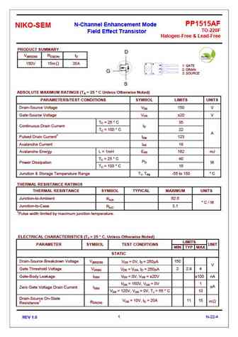
PP1515AF N-Channel Enhancement Mode NIKO-SEM TO-220F Field Effect Transistor Halogen-Free & Lead-Free PRODUCT SUMMARY D V(BR)DSS RDS(ON) ID 150V 15m 35A 1 GATE 2 DRAIN G 3 SOURCE S ABSOLUTE MAXIMUM RATINGS (TA = 25 C Unless Otherwise Noted) PARAMETERS/TEST CONDITIONS SYMBOL LIMITS UNITS Drain-Source Voltage VDS 150 V Gate-Source Voltage VGS 20 V TC
0.13. Size:977K cn twgmc
tw1515asi.pdf 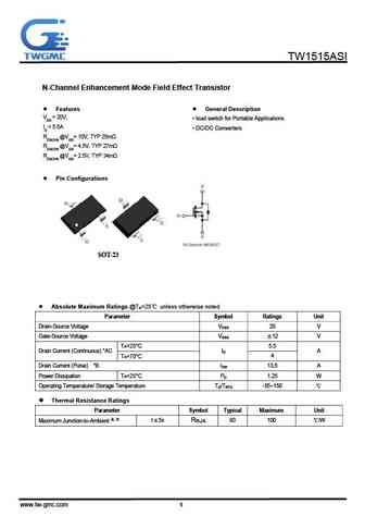
TW1515ASI AO3400 SI2305 N-Channel Enhancement Mode Field Effect Transistor Features General Description VDS = 20V, load switch for Portable Applications ID = 5.5A DC/DC Converters RDS(ON) @VGS= 10V, TYP 25m RDS(ON) @VGS= 4.5V, TYP 27m RDS(ON) @VGS= 2.5V, TYP 34m Pin Configurations SOT-23 Absolute Maximum Ratings @T =25 unless otherwise
0.14. Size:208K inchange semiconductor
2sd1515.pdf 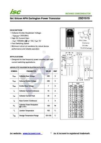
INCHANGE Semiconductor isc Silicon NPN Darlington Power Transistor 2SD1515 DESCRIPTION Collector-Emitter Breakdown Voltage- V = 200V(Min) (BR)CEO High DC Current Gain h = 1000(Min) @ I = 10A, V = 3V FE C CE Fast Switching Speed Minimum Lot-to-Lot variations for robust device performance and reliable operation APPLICATIONS Designed for low frequency power amplifier and
0.15. Size:202K inchange semiconductor
2sk1515.pdf 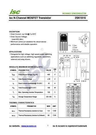
isc N-Channel MOSFET Transistor 2SK1515 ESCRIPTION Drain Current I =10A@ T =25 D C Drain Source Voltage- V =450 (Min) DSS Minimum Lot-to-Lot variations for robust device performance and reliable operation APPLICATIONS Designed for high voltage, high speed power switching applications such as switching regulators, converters, solenoid and relay drivers. ABSOLUTE MAXI
Другие IGBT... SSS12N60, SSS1N60, SSS2N60, SSS5N60, SSS7N60, SSS8N60, 1002, 1115, SI2302, G1601, 2300, 2301, 2302, 3035, 3400, 3401, 3415
