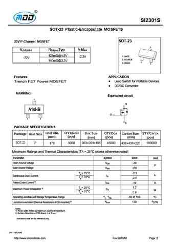
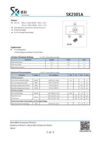
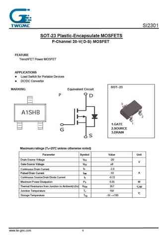
2301 datasheet, аналоги, основные параметры
Наименование производителя: 2301 📄📄
Тип транзистора: MOSFET
Полярность: P
Предельные значения
Pd ⓘ - Максимальная рассеиваемая мощность: 1 W
|Vds|ⓘ - Максимально допустимое напряжение сток-исток: 20 V
|Vgs|ⓘ - Максимально допустимое напряжение затвор-исток: 12 V
|Id| ⓘ - Максимально допустимый постоянный ток стока: 3 A
Tj ⓘ - Максимальная температура канала: 150 °C
Электрические характеристики
tr ⓘ - Время нарастания: 35 ns
Cossⓘ - Выходная емкость: 75 pf
RDSonⓘ - Сопротивление сток-исток открытого транзистора: 0.11 Ohm
Тип корпуса: SOT23
📄📄 Копировать
Аналог (замена) для 2301
- подборⓘ MOSFET транзистора по параметрам
2301 даташит
2301.pdf
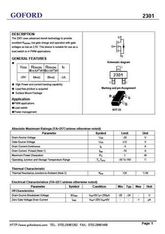
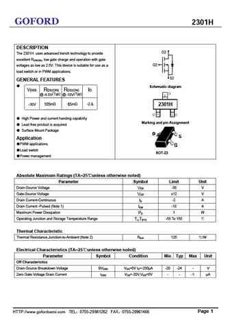
GOFORD 2301 DESCRIPTION D The 2301 uses advanced trench technology to provide excellent RDS(ON), low gate charge and operation with gate G voltages as low as 2.5V. This device is suitable for use as a load switch or in PWM applications. S GENERAL FEATURES Schematic diagram VDSS RDS(ON) RDS(ON) ID (Typ) @-2.5V @-4.5V (Typ) -20V 64m 89 m -3 A High Power a
2301.pdf
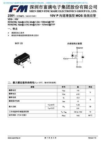
FM , FM WWW.SZLCSC.COM, SHEN ZHEN FINE MADE ELECTRONICS GROUP CO., LTD. 2301 S&CIC1596 10V P MOS VDS= -10V RDS(ON), Vgs@-4.5V, Ids@-1.0A =100m @TYP RDS(ON), Vgs@-2.5V,
rn2301 rn2302 rn2303 rn2304 rn2305 rn2306.pdf
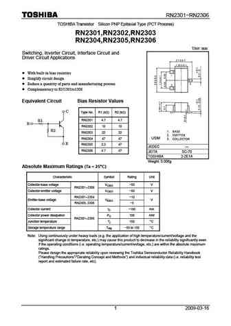
RN2301 RN2306 TOSHIBA Transistor Silicon PNP Epitaxial Type (PCT Process) RN2301,RN2302,RN2303 RN2304,RN2305,RN2306 Unit mm Switching, Inverter Circuit, Interface Circuit and Driver Circuit Applications With built-in bias resistors Simplify circuit design Reduce a quantity of parts and manufacturing process Complementary to RN1301to1306 Equivalent Circuit Bias Resi
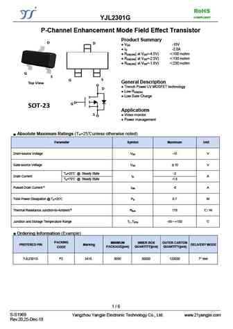
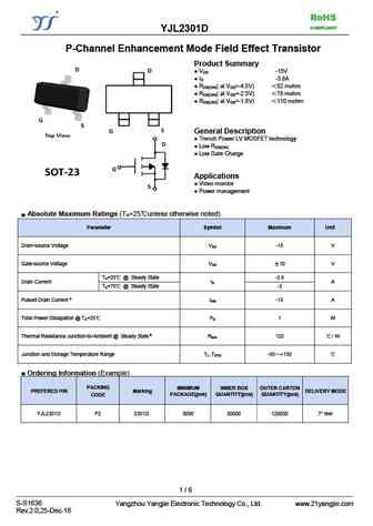
nx2301p.pdf
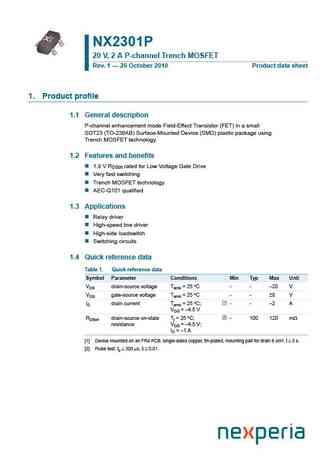
NX2301P 20 V, 2 A P-channel Trench MOSFET Rev. 1 26 October 2010 Product data sheet 1. Product profile 1.1 General description P-channel enhancement mode Field-Effect Transistor (FET) in a small SOT23 (TO-236AB) Surface-Mounted Device (SMD) plastic package using Trench MOSFET technology. 1.2 Features and benefits 1.8 V RDSon rated for Low Voltage Gate Drive Very fast switching
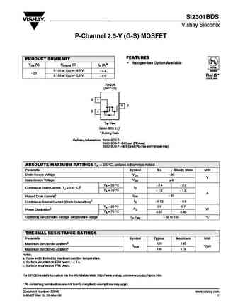
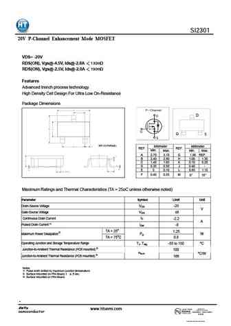
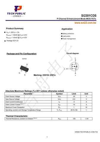
si2301ds.pdf
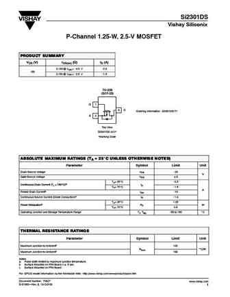
Si2301DS Vishay Siliconix P-Channel 1.25-W, 2.5-V MOSFET PRODUCT SUMMARY VDS (V) rDS(on) (W) ID (A) 0.130 @ VGS = - 4.5 V -2.3 -20 20 0.190 @ VGS = - 2.5 V -1.9 TO-236 (SOT-23) G 1 3 D Ordering Information Si2301DS-T1 S 2 Top View Si2301DS (A1)* *Marking Code ABSOLUTE MAXIMUM RATINGS (TA = 25_C UNLESS OTHERWISE NOTED) Parameter Symbol Limit Unit Drain-Source Voltage VDS -20
si2301cd.pdf

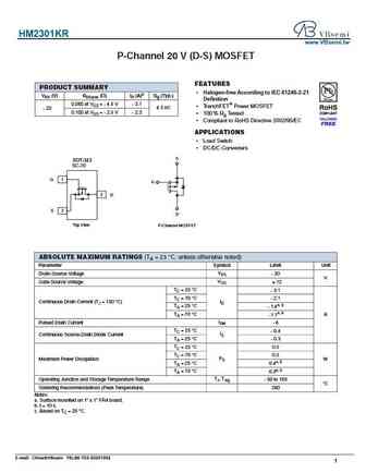
Si2301CDS Vishay Siliconix P-Channel 20 V (D-S) MOSFET FEATURES MOSFET PRODUCT SUMMARY Halogen-free According to IEC 61249-2-21 VDS (V) RDS(on) ( ) ID (A)a Qg (Typ.) Definition 0.112 at VGS = - 4.5 V - 3.1 TrenchFET Power MOSFET - 20 3.3 nC Compliant to RoHS Directive 2002/95/EC 0.142 at VGS = - 2.5 V - 2.7 APPLICATIONS Load Switch TO-236 (SOT-23) G
si2301cds.pdf
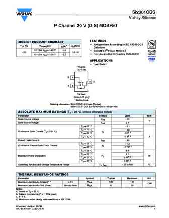
Si2301CDS Vishay Siliconix P-Channel 20 V (D-S) MOSFET FEATURES MOSFET PRODUCT SUMMARY Halogen-free According to IEC 61249-2-21 VDS (V) RDS(on) ( ) ID (A)a Qg (Typ.) Definition 0.112 at VGS = - 4.5 V - 3.1 TrenchFET Power MOSFET - 20 3.3 nC Compliant to RoHS Directive 2002/95/EC 0.142 at VGS = - 2.5 V - 2.7 APPLICATIONS Load Switch TO-236 (SOT-23) G
si2301-tp.pdf
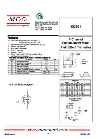
MCC Micro Commercial Components TM 20736 Marilla Street Chatsworth Micro Commercial Components CA 91311 SI2301 Phone (818) 701-4933 Fax (818) 701-4939 Features P-Channel -20V,-2.8A, RDS(ON)=120m @VGS=-4.5V RDS(ON)=150m @VGS=-2.5V Enhancement Mode High dense cell design for extremely low RDS(ON) Rugged and reliable Field Effect Transistor High Sp
si2301ads.pdf
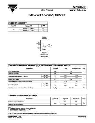
Si2301ADS New Product Vishay Siliconix P-Channel 2.5-V (G-S) MOSFET PRODUCT SUMMARY VDS (V) rDS(on) (W) ID (A)b 0.130 @ VGS = 4.5 V 2.0 20 0.190 @ VGS = 2.5 V 1.6 TO-236 (SOT-23) G 1 3 D S 2 Top View Si2301DS (1A)* *Marking Code ABSOLUTE MAXIMUM RATINGS (TA = 25_C UNLESS OTHERWISE NOTED) Parameter Symbol 5 sec Steady State Unit Drain-Source Voltage VDS 20 V
sq2301es.pdf
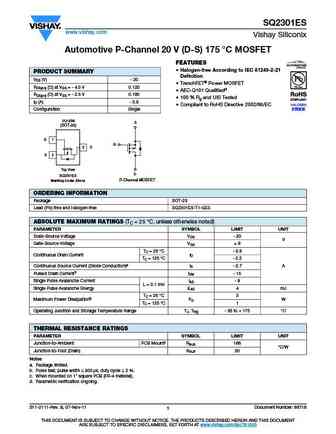
SQ2301ES www.vishay.com Vishay Siliconix Automotive P-Channel 20 V (D-S) 175 C MOSFET FEATURES Halogen-free According to IEC 61249-2-21 PRODUCT SUMMARY Definition VDS (V) - 20 TrenchFET Power MOSFET RDS(on) ( ) at VGS = - 4.5 V 0.120 AEC-Q101 Qualifiedd RDS(on) ( ) at VGS = - 2.5 V 0.180 100 % Rg and UIS Tested ID (A) - 3.9 Compliant to RoHS Directive
si2301bds.pdf
Si2301BDS Vishay Siliconix P-Channel 2.5-V (G-S) MOSFET FEATURES PRODUCT SUMMARY Halogen-free Option Available VDS (V) RDS(on) ( ) ID (A)b Pb-free 0.100 at VGS = - 4.5 V Available - 2.4 - 20 0.150 at VGS = - 2.5 V RoHS* - 2.0 COMPLIANT TO-236 (SOT-23) G 1 3 D S 2 Top View Si2301 BDS (L1)* * Marking Code Ordering Information Si2301BDS-T1 Si2301BDS-T1-E3 (Lead (Pb)
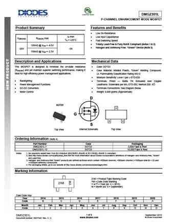
dmg2301lk.pdf
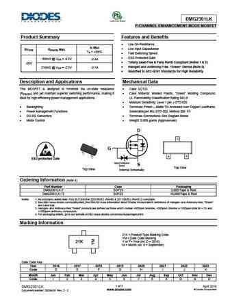
DMG2301LK P-CHANNEL ENHANCEMENT MODE MOSFET Product Summary Features and Benefits Low On-Resistance ID Max Low Input Capacitance BVDSS RDS(ON) Max TA = +25 C Fast Switching Speed ESD Protected Gate 160m @ VGS = -4.5V -2.4A Totally Lead-Free & Fully RoHS Compliant (Notes 1 & 2) -20V Halogen and Antimony Free. Green Device (Note 3) 210
dmg2301u.pdf
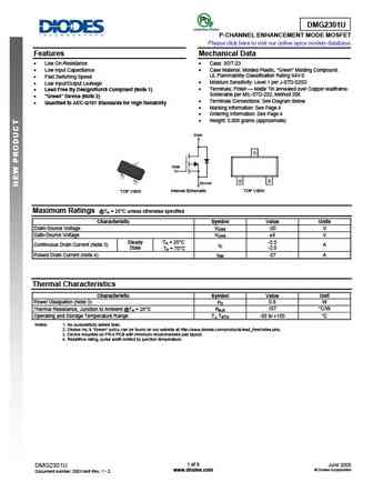
DMG2301U P-CHANNEL ENHANCEMENT MODE MOSFET Please click here to visit our online spice models database. Features Mechanical Data Low On-Resistance Case SOT-23 Low Input Capacitance Case Material Molded Plastic, Green Molding Compound. UL Flammability Classification Rating 94V-0 Fast Switching Speed Moisture Sensitivity Level 1 per J-STD-020D L
zxtn23015cfh.pdf
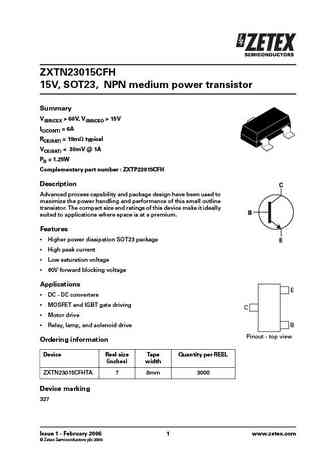
ZXTN23015CFH 15V, SOT23, NPN medium power transistor Summary V(BR)CEX > 60V, V(BR)CEO > 15V IC(CONT) = 6A RCE(SAT) = 19m typical VCE(SAT)
zxtp23015cfh.pdf
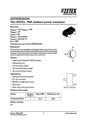
ZXTP23015CFH 15V, SOT23, PNP medium power transistor Summary V(BR)CES > -15V, V(BR)CEO > -15V V(BR)ECO > -6V IC(CONT) = -6A RCE(SAT) = 20m typical VCE(SAT)
dmg2301l.pdf
DMG2301L P-CHANNEL ENHANCEMENT MODE MOSFET Product Summary Features and Benefits Low On-Resistance ID max Low Input Capacitance V(BR)DSS RDS(ON) max TA = +25 C Fast Switching Speed Totally Lead-Free & Fully RoHS Compliant (Notes 1 & 2) 120m @ VGS = -4.5V Halogen and Antimony Free. Green Device (Note 3) -20V -3A 150m @ VGS = -2.5V De
sil2301.pdf
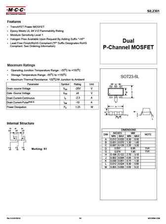
SIL2301 Features TrenchFET Power MOSFET Epoxy Meets UL 94 V-0 Flammability Rating Moisture Sensitivity Level 1 Halogen Free Available Upon Request By Adding Suffix "-HF" Dual Lead Free Finish/RoHS Compliant ("P" Suffix Designates RoHS Compliant. See Ordering Information) P-Channel MOSFET Maximum Ratings Operating Junction Temperature Range -55oC to +150oC
si2301.pdf

MCC Micro Commercial Components TM 20736 Marilla Street Chatsworth Micro Commercial Components CA 91311 SI2301 Phone (818) 701-4933 Fax (818) 701-4939 Features P-Channel -20V,-2.8A, RDS(ON)=120m @VGS=-4.5V RDS(ON)=150m @VGS=-2.5V Enhancement Mode High dense cell design for extremely low RDS(ON) Rugged and reliable Field Effect Transistor High Sp
ut2301.pdf
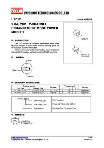
UNISONIC TECHNOLOGIES CO., LTD UT2301 Power MOSFET 2.8A, 20V P-CHANNEL ENHANCEMENT MODE POWER MOSFET DESCRIPTION The UTC UT2301 is P-channel enhancement mode power MOSFET, designed in serried ranks. With fast switching speed, low on-resistance, favorable stabilization. Used in commercial and industrial surface mount applications and suited for low voltage applications su
ut2301g-ae2-r ut2301g-ae3-r.pdf
UNISONIC TECHNOLOGIES CO., LTD UT2301 Power MOSFET Y2.8A, 20V P-CHANNEL ENHANCEMENT MODE POWER MOSFET DESCRIPTION The UTC UT2301 is P-channel enhancement mode power MOSFET, designed in serried ranks. With fast switching speed, low on-resistance, favorable stabilization. Used in commercial and industrial surface mount applications and suited for low voltage applications s
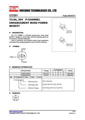
ut2301z.pdf
UNISONIC TECHNOLOGIES CO., LTD UT2301Z Power MOSFET 2.3A, 20V P-CHANNEL ENHANCEMENT MODE POWER MOSFET DESCRIPTION The UTC UT2301Z is a P-channel enhancement mode power MOSFET with fast switching speed, low on-resistance and favorable stabilization. It can be used in commercial and industrial surface mount applications and suited for low voltage applications such as DC/DC co
smg2301p.pdf
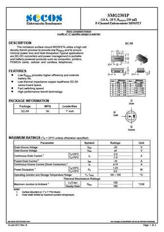
SMG2301P -2.6 A, -20 V, RDS(ON) 130 m P-Channel Enhancement MOSFET Elektronische Bauelemente RoHS Compliant Product A suffix of -C specifies halogen & lead-free DESCRIPTION SC-59 The miniature surface mount MOSFETs utilize a high cell density trench process to provide low RDS(on) and to ensure A L minimal power loss and heat dissipation.Typical applications 3 3
smg2301.pdf
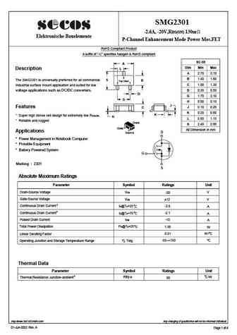
SMG2301 -2.6A, -20V,RDS(ON) 130m Elektronische Bauelemente P-Channel Enhancement Mode Power Mos.FET RoHS Compliant Product A suffix of "-C" specifies halogen & RoHS compliant SC-59 A Dim Min Max Description L A 2.70 3.10 3 B 1.40 1.60 The SMG2301 is universally preferred for all commercial S B Top View 2 1 C 1.00 1.30 industrial surface mount application and suited for l
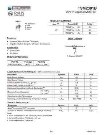
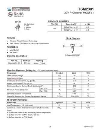
tsm2301a.pdf
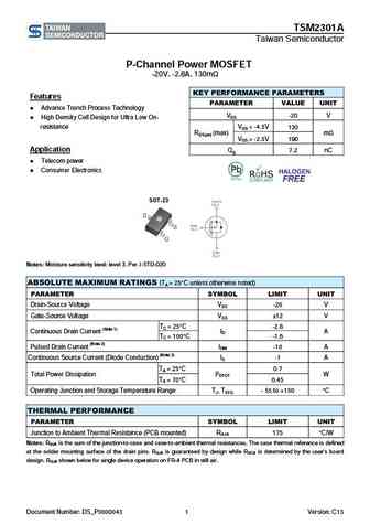
TSM2301A Taiwan Semiconductor P-Channel Power MOSFET -20V, -2.8A, 130m KEY PERFORMANCE PARAMETERS Features PARAMETER VALUE UNIT Advance Trench Process Technology VDS -20 V High Density Cell Design for Ultra Low On- resistance VGS = -4.5V 130 RDS(on) (max) m VGS = -2.5V 190 Application Qg 7.2 nC Telecom power Consumer Electronics SOT-23
tsm2301acx tsm2301cx.pdf
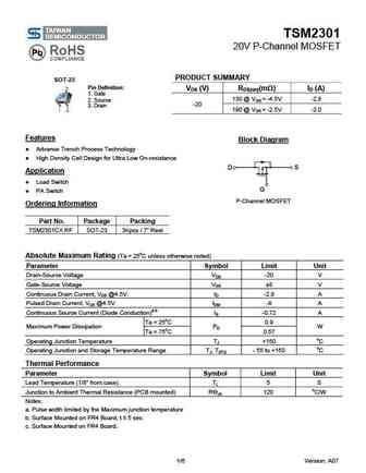
TSM2301 20V P-Channel MOSFET PRODUCT SUMMARY SOT-23 Pin Definition VDS (V) RDS(on)(m ) ID (A) 1. Gate 130 @ VGS = -4.5V -2.8 2. Source -20 3. Drain 190 @ VGS = -2.5V -2.0 Features Block Diagram Advance Trench Process Technology High Density Cell Design for Ultra Low On-resistance Application Load Switch PA Switch P-Channel MOSFET Orderi
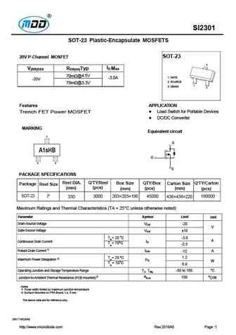
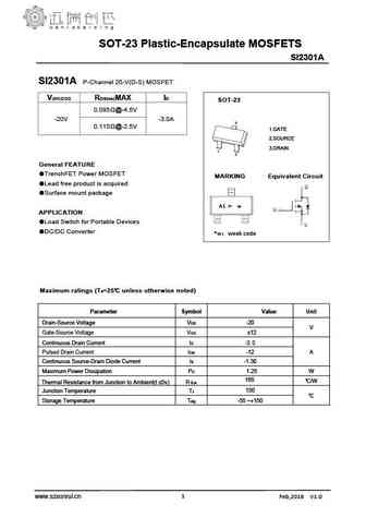
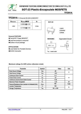
cj2301.pdf
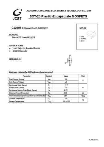
JIANGSU CHANGJIANG ELECTRONICS TECHNOLOGY CO., LTD SOT-23 Plastic-Encapsulate MOSFETS CJ2301 P-Channel 20-V(D-S) MOSFET SOT-23 FEATURE 1. GATE TrenchFET Power MOSFET 2. SOURCE 3. DRAIN APPLICATIONS z Load Switch for Portable Devices z DC/DC Converter MARKING S1 Maximum ratings (Ta=25 unless otherwise noted) Parameter Symbol Value Unit Drain-Source Voltage VDS -20
cj2301s.pdf
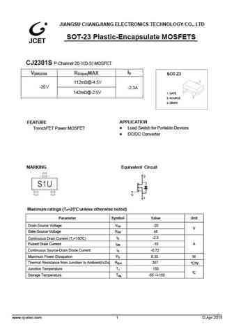
JIANGSU CHANGJIANG ELECTRONICS TECHNOLOGY CO., LTD SOT-23 Plastic-Encapsulate MOSFETS CJ2301S P-Channel 20-V(D-S) MOSFET ID V(BR)DSS RDS(on)MAX SOT-23 112m @-4.5V -20V -2.3A 142m @-2.5V 1. GATE 2. SOURCE 3. DRAIN APPLICATION FEATURE z Load Switch for Portable Devices TrenchFET Power MOSFET z DC/DC Converter MARKING Equivalent Circuit Maximum ratings (Ta
cjl2301.pdf
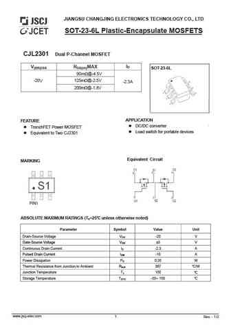
JIANGSU CHANGJING ELECTRONICS TECHNOLOGY CO., LTD SOT-23-6L Plastic-Encapsulate MOSFETS CJL2301 Dual P-Channel MOSFET ID V(BR)DSS RDS(on)MAX SOT-23-6L 90m @-4.5V 125m @-2.5V -20 V -2.3A 200m @-1.8V APPLICATION FEATURE DC/DC converter TrenchFET Power MOSFET Load switch for portable devices Equivalent to Two CJ2301 Equivalent Circuit MARKING
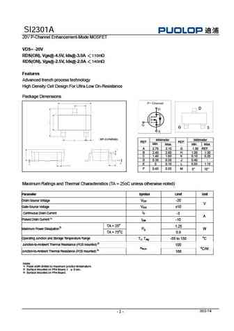
si2301.pdf
SI2301 20V P-Channel Enhancement Mode MOSFET VDS= -20V RDS(ON), Vgs@-4.5V, Ids@-2.8A 130m RDS(ON), Vgs@-2.5V, Ids@-2.0A 190m Features Advanced trench process technology High Density Cell Design For Ultra Low On-Resistance Package Dimensions D G S SOT-23(PACKAGE) Millimeter Millimeter REF. REF. Min. Max. Min. Max. A 2.70 3.10 G 1.90 REF. B 2.40 2.80 H 1.00 1.30
ces2301.pdf
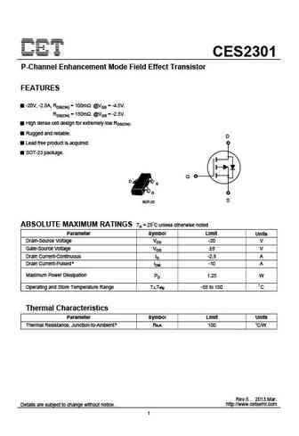
CES2301 P-Channel Enhancement Mode Field Effect Transistor FEATURES -20V, -2.8A, RDS(ON) = 100m @VGS = -4.5V. RDS(ON) = 150m @VGS = -2.5V. High dense cell design for extremely low RDS(ON). Rugged and reliable. D Lead free product is acquired. SOT-23 package. G D S G S SOT-23 ABSOLUTE MAXIMUM RATINGS TA = 25 C unless otherwise noted Parameter Symbol Limit Units Drain-Sou
cen2301.pdf
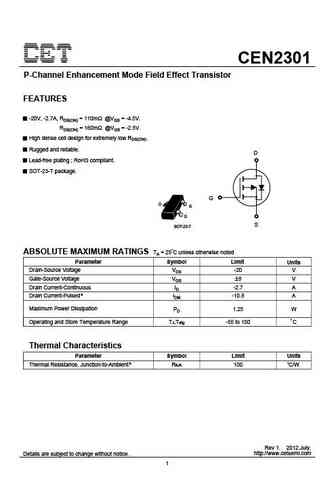
CEN2301 P-Channel Enhancement Mode Field Effect Transistor FEATURES -20V, -2.7A, RDS(ON) = 110m @VGS = -4.5V. RDS(ON) = 160m @VGS = -2.5V. High dense cell design for extremely low RDS(ON). Rugged and reliable. D Lead-free plating ; RoHS compliant. SOT-23-T package. G D S G S SOT-23-T ABSOLUTE MAXIMUM RATINGS TA = 25 C unless otherwise noted Parameter Symbol Limit Units

gm2301.pdf
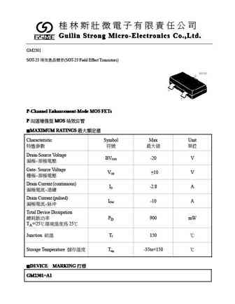
Guilin Strong Micro-Electronics Co.,Ltd. Guilin Strong Micro-Electronics Co.,Ltd. Guilin Strong Micro-Electronics Co.,Ltd. Guilin Strong Micro-Electronics Co.,Ltd. GM2301 SOT-23 (SOT-23 Field Effect Transistors) P-Channel Enhancement-Mode MOS FETs P-Channel Enhancement-Mode MOS FETs P-Channel Enhancement-Mode MOS FET
wtc2301.pdf
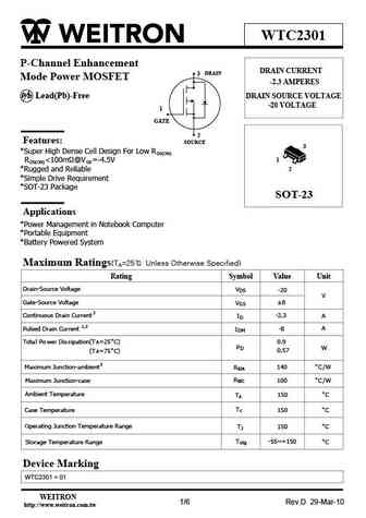
WTC2301 P-Channel Enhancement DRAIN CURRENT 3 DRAIN Mode Power MOSFET -2.3 AMPERES P b Lead(Pb)-Free DRAIN SOURCE VOLTAGE -20 VOLTAGE 1 GATE 2 Features SOURCE 3 *Super High Dense Cell Design For Low RDS(ON) 1 RDS(ON)
se2301.pdf
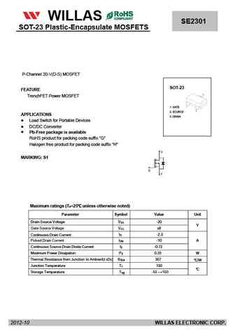
FM120-M WILLAS SE2301THRU SOT-23 Plastic-Encapsulate MOSFETS FM1200-M 1.0A SURFACE MOUNT SCHOTTKY BARRIER RECTIFIERS -20V- 200V SOD-123 PACKAGE Pb Free Product Package outline Features Batch process design, excellent power dissipation offers better reverse leakage current and thermal resistance. SOD-123H Low profile surface mounted application in order to optimize
h2301n.pdf
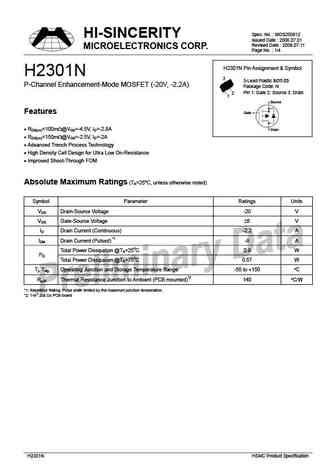
Spec. No. MOS200612 HI-SINCERITY Issued Date 2006.07.01 Revised Date 2006.07.11 MICROELECTRONICS CORP. Page No. 1/4 H2301N Pin Assignment & Symbol H2301N 3 3-Lead Plastic SOT-23 P-Channel Enhancement-Mode MOSFET (-20V, -2.2A) Package Code N Pin 1 Gate 2 Source 3 Drain 2 1 Source Features Gate Drain RDS(on)
aoca32301.pdf
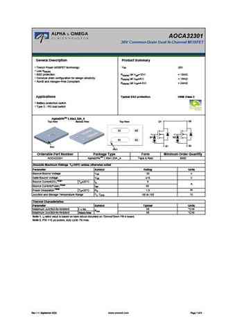
AOCA32301 30V Common-Drain Dual N-Channel MOSFET General Description Product Summary VSS Trench Power MOSFET technology 30V Low RSS(ON) ESD protection RSS(ON) (at VGS=10V)
ap2301agn.pdf
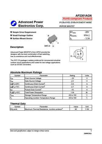
AP2301AGN RoHS-compliant Product Advanced Power P-CHANNEL ENHANCEMENT MODE Electronics Corp. POWER MOSFET Simple Drive Requirement BVDSS -20V Small Package Outline RDS(ON) 97m D Surface Mount Device ID - 3.3A S SOT-23 G Description D Advanced Power MOSFETs from APEC provide the designer with the best combination of fast switching, G low on-resistance and cost-effec
ap2301agn-hf.pdf
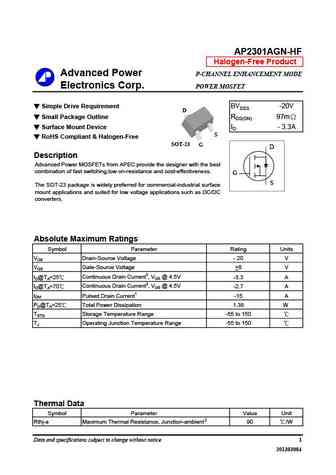
AP2301AGN-HF Halogen-Free Product Advanced Power P-CHANNEL ENHANCEMENT MODE Electronics Corp. POWER MOSFET Simple Drive Requirement BVDSS -20V D Small Package Outline RDS(ON) 97m Surface Mount Device ID - 3.3A S RoHS Compliant & Halogen-Free SOT-23 G D Description Advanced Power MOSFETs from APEC provide the designer with the best combination of fast switching,l
ap2301gn.pdf
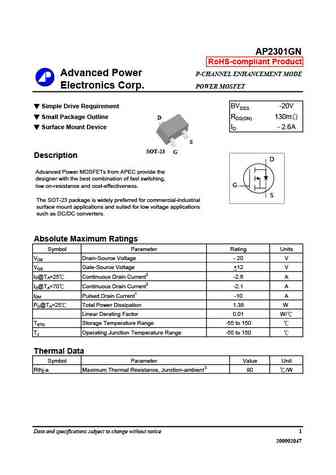
AP2301GN RoHS-compliant Product Advanced Power P-CHANNEL ENHANCEMENT MODE Electronics Corp. POWER MOSFET Simple Drive Requirement BVDSS -20V Small Package Outline RDS(ON) 130m D Surface Mount Device ID - 2.6A S SOT-23 G Description D Advanced Power MOSFETs from APEC provide the designer with the best combination of fast switching, G low on-resistance and cost-effec
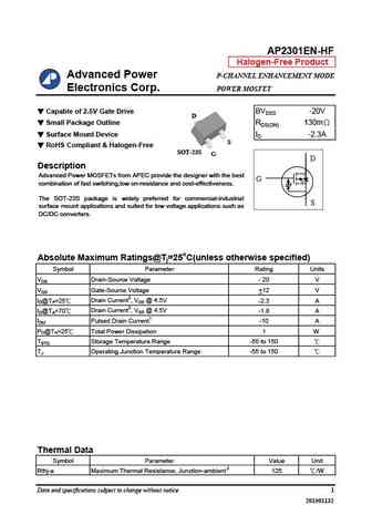
ap2301en-hf.pdf
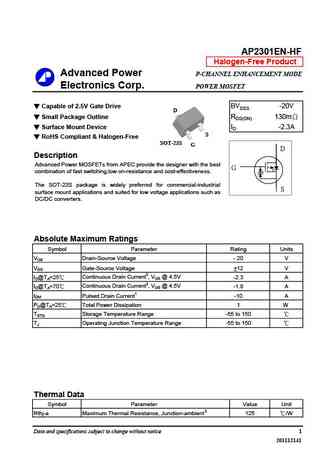
AP2301EN-HF Halogen-Free Product Advanced Power P-CHANNEL ENHANCEMENT MODE Electronics Corp. POWER MOSFET Capable of 2.5V Gate Drive BVDSS -20V D Small Package Outline RDS(ON) 130m Surface Mount Device ID -2.3A S RoHS Compliant & Halogen-Free SOT-23S G D Description Advanced Power MOSFETs from APEC provide the designer with the best G combination of fast switch
ap2301bgn-hf.pdf
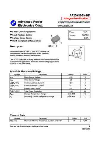
AP2301BGN-HF Halogen-Free Product Advanced Power P-CHANNEL ENHANCEMENT MODE Electronics Corp. POWER MOSFET Simple Drive Requirement BVDSS -20V Small Package Outline RDS(ON) 130m D Surface Mount Device ID - 2.8A RoHS Compliant & Halogen-Free S SOT-23 G Description D Advanced Power MOSFETs from APEC provide the designer with the best combination of fast switching,
ap2301gn-hf.pdf
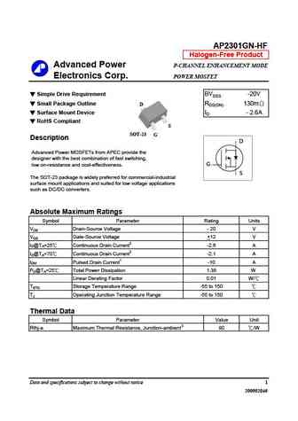
AP2301GN-HF Halogen-Free Product Advanced Power P-CHANNEL ENHANCEMENT MODE Electronics Corp. POWER MOSFET Simple Drive Requirement BVDSS -20V Small Package Outline RDS(ON) 130m D Surface Mount Device ID - 2.6A RoHS Compliant S SOT-23 G Description D Advanced Power MOSFETs from APEC provide the designer with the best combination of fast switching, G low on-resi
ap2301n-hf.pdf

AP2301N-HF Halogen-Free Product Advanced Power P-CHANNEL ENHANCEMENT MODE Electronics Corp. POWER MOSFET Capable of 2.5V Gate Drive BVDSS -20V D Small Package Outline RDS(ON) 130m Surface Mount Device ID -2.3A S RoHS Compliant & Halogen-Free SOT-23S G D Description Advanced Power MOSFETs from APEC provide the designer with the best G combination of fast switchi
ap2301en.pdf
AP2301EN-HF Halogen-Free Product Advanced Power P-CHANNEL ENHANCEMENT MODE Electronics Corp. POWER MOSFET Capable of 2.5V Gate Drive BVDSS -20V D Small Package Outline RDS(ON) 130m Surface Mount Device ID -2.3A S RoHS Compliant & Halogen-Free SOT-23S G D Description Advanced Power MOSFETs from APEC provide the designer with the best G combination of fast switch
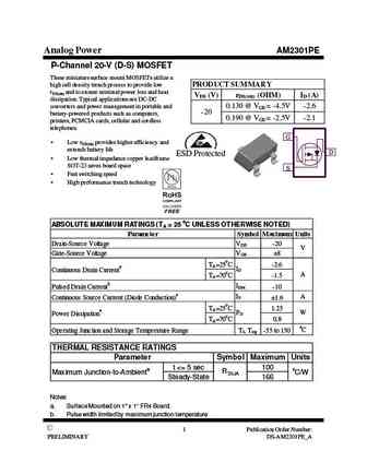
am2301p.pdf
Analog Power AM2301P P-Channel 20-V (D-S) MOSFET PRODUCT SUMMARY Key Features rDS(on) (m ) VDS (V) ID (A) Low r trench technology DS(on) 130 @ VGS = -4.5V -2.6 Low thermal impedance -20 190 @ VGS = -2.5V -2.2 Fast switching speed SOT-23 Typical Applications Load Switches DC/DC Conversion Motor Drives ABSOLUTE MAXIMUM RATINGS (TA = 25 C UNLE
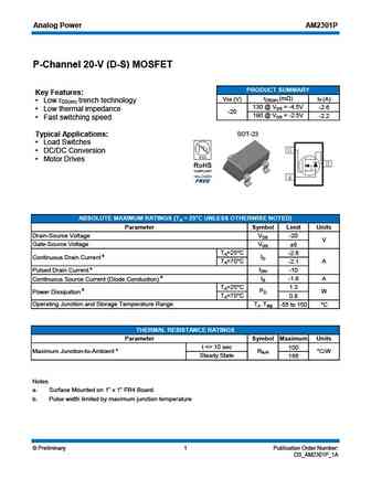
am2301pe.pdf
Analog Power AM2301PE P-Channel 20-V (D-S) MOSFET These miniature surface mount MOSFETs utilize a high cell density trench process to provide low PRODUCT SUMMARY rDS(on) and to ensure minimal power loss and heat VDS (V) rDS(on) (OHM) ID (A) dissipation. Typical applications are DC-DC converters and power management in portable and 0.130 @ VGS = -4.5V -2.6 -20 battery-powered product
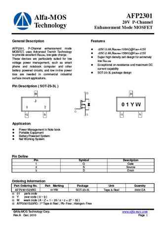
afp2301s.pdf
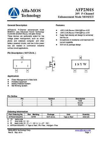
AFP2301S Alfa-MOS 20V P-Channel Technology Enhancement Mode MOSFET General Description Features AFP2301S, P-Channel enhancement mode -20V/-2.8A,RDS(ON)=120m @VGS=-4.5V MOSFET, uses Advanced Trench Technology -20V/-2.0A,RDS(ON)=170m @VGS=-2.5V to provide excellent RDS(ON), low gate charge. Super high density cell design for extremely These devices are particularly
afp2301.pdf
AFP2301 Alfa-MOS 20V P-Channel Technology Enhancement Mode MOSFET General Description Features AFP2301, P-Channel enhancement mode -20V/-3.0A,RDS(ON)=105m @VGS=-4.5V MOSFET, uses Advanced Trench Technology -20V/-2.4A,RDS(ON)=155m @VGS=-2.5V to provide excellent RDS(ON), low gate charge. Super high density cell design for extremely These devices are particularly su
afp2301as.pdf
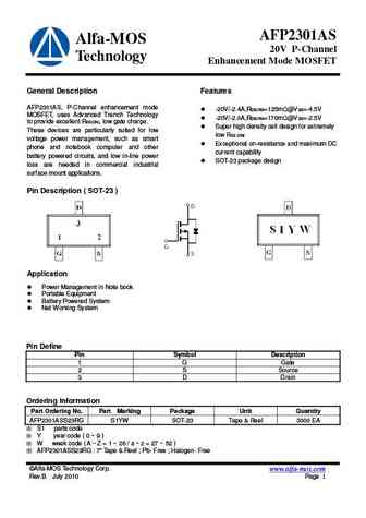
AFP2301AS Alfa-MOS 20V P-Channel Technology Enhancement Mode MOSFET General Description Features AFP2301AS, P-Channel enhancement mode -20V/-2.4A,RDS(ON)=125m @VGS=-4.5V MOSFET, uses Advanced Trench Technology -20V/-2.0A,RDS(ON)=170m @VGS=-2.5V to provide excellent RDS(ON), low gate charge. Super high density cell design for extremely These devices are particularl
afp2301a.pdf

AFP2301A Alfa-MOS 20V P-Channel Technology Enhancement Mode MOSFET General Description Features AFP2301A, P-Channel enhancement mode -20V/-2.6A,RDS(ON)=120m @VGS=-4.5V MOSFET, uses Advanced Trench Technology -20V/-2.2A,RDS(ON)=170m @VGS=-2.5V to provide excellent RDS(ON), low gate charge. Super high density cell design for extremely These devices are particularly
si2301a.pdf
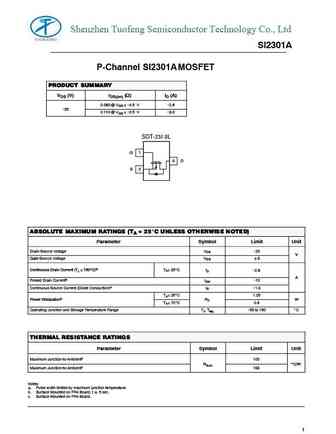
Shenzhen Tuofeng Semiconductor Technology Co., Ltd Sl2301A P-Channel SI2301AMOSFET PRODUCT SUMMARY VDS (V) rDS(on) (W) ID (A) 0.080 @ VGS = -4.5 V -2.8 -20 20 0.110 @ VGS = -2.5 V -2.0 SOT-23/-3L G 1 3 D S 2 ABSOLUTE MAXIMUM RATINGS (TA = 25_C UNLESS OTHERWISE NOTED) Parameter Symbol Limit Unit Drain-Source Voltage VDS -20 V V Gate-Source Voltage VGS "8 Continuous Drain Curr
si2301 a1shb.pdf
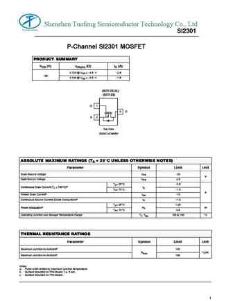
Shenzhen Tuofeng Semiconductor Technology Co., Ltd SI2301 P-Channel SI2301 MOSFET PRODUCT SUMMARY VDS (V) rDS(on) (W) ID (A) 0.120 @ VGS = -4.5 V -2.8 -20 20 0.190 @ VGS = -2.5 V -1.8 (SOT-23-3L) (SOT-23) G 1 3 D S 2 Top View SI2301(A1sHB)* ABSOLUTE MAXIMUM RATINGS (TA = 25_C UNLESS OTHERWISE NOTED) Parameter Symbol Limit Unit Drain-Source Voltage VDS -20 V V Gate-Source V
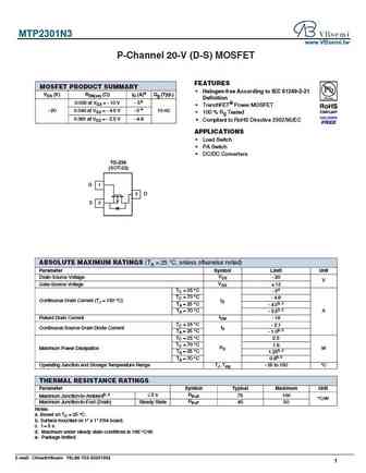
mtp2301n3.pdf
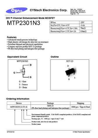
Spec. No. C322N3 CYStech Electronics Corp. Issued Date 2004.04.05 Revised Date 2018.08.31 Page No. 1/9 20V P-Channel Enhancement Mode MOSFET BVDSS -20V MTP2301N3 ID@TA=25 C, VGS=-4.5V -3.4A 79m RDSON(TYP)@VGS=-4.5V, ID=-2.8A 116m RDSON(TYP)@VGS=-2.5V, ID=-2A Features Advanced trench process technology High density cell design for ultra low on res
mtp2301s3.pdf
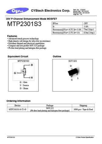
Spec. No. C322S3 CYStech Electronics Corp. Issued Date 2013.08.29 Revised Date 2013.09.09 Page No. 1/8 20V P-Channel Enhancement Mode MOSFET BVDSS -20V MTP2301S3 ID -1.6A 75m (typ.) RDSON(MAX)@VGS=-4.5V, ID=-1.6A 113m (typ.) RDSON(MAX)@VGS=-2.5V, ID=-1A Features Advanced trench process technology High density cell design for ultra low on resistance
2301l.pdf
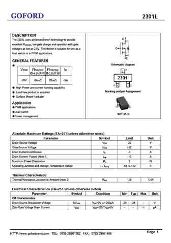
GOFORD 2301L DESCRIPTION D The 2301L uses advanced trench technology to provide excellent RDS(ON), low gate charge and operation with gate G voltages as low as 2.5V. This device is suitable for use as a load switch or in PWM applications. S GENERAL FEATURES Schematic diagram VDSS RDS(ON) RDS(ON) ID (Typ) @-2.5V @-4.5V (Typ) -20V 64m 89 m -3 A High Power
sts2301a.pdf
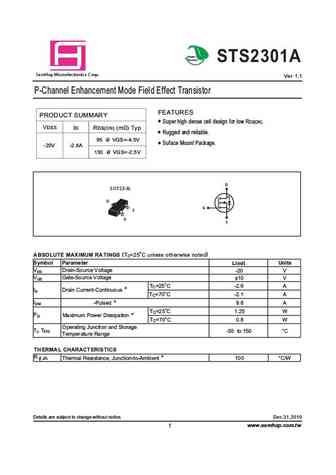
Green Product STS2301A a S mHop Microelectronics C orp. Ver 1.1 P-Channel Enhancement Mode Field Effect Transistor FEATURES PRODUCT SUMMARY Super high dense cell design for low RDS(ON). VDSS ID RDS(ON) (m ) Typ Rugged and reliable. 95 @ VGS=-4.5V Suface Mount Package. -20V -2.6A 130 @ VGS=-2.5V D S OT23-3L D G S G S (TC=25 C unless otherwise noted) ABSOLUTE MAXIMUM RAT
sts2301.pdf
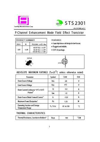
Green Product S TS 2301 S amHop Microelectronics C orp. J UL.30 2004 ver1.1 P-Channel E nhancement Mode Field E ffect Transistor PR ODUC T S UMMAR Y F E ATUR E S S uper high dense cell design for low R DS (ON). VDS S ID R DS (ON) ( m ) Max R ugged and reliable. 60 @ VG S = -4.5V -20V -3.4A 80 @ VG S = -2.5V S OT-23 package. 105 @ VG S = -1.8V D S OT-23 G S AB S OLUTE MAXI
ssf2301b.pdf
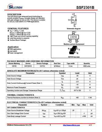
SSF2301B D DESCRIPTION The SSF2301B uses advanced trench technology to provide excellent RDS(ON), low gate charge and operation with gate voltages as low as 2.5V. This device is suitable G for use as a load switch or in PWM applications. S Schematic diagram GENERAL FEATURES VDS = -20V,ID = -2.8A RDS(ON)
ssf2301a.pdf
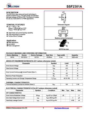
SSF2301A D DESCRIPTION The SSF2301A uses advanced trench technology to provide excellent RDS(ON), low gate charge and operation with gate voltages as low as 2.5V. This device is suitable G for use as a load switch or in PWM applications. S Schematic diagram GENERAL FEATURES VDS = -20V,ID = -4A RDS(ON)
ssf2301.pdf
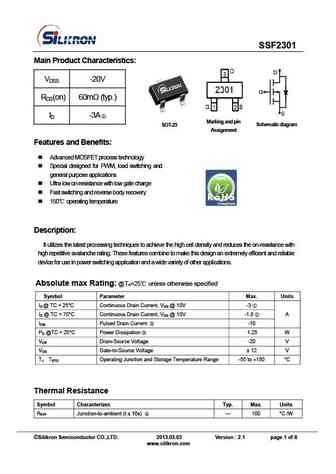
SSF2301 Main Product Characteristics D VDSS -20V G RDS(on) 60m (typ.) S ID -3A Marking and pin SOT-23 Schematic diagram Assignme nt Features and Benefits Advanced MOSFET process technology Special designed for PWM, load switching and general purpose applications Ultra low on-resistance with low gate charge Fast switching and reverse body re
cs2301 sot-23.pdf
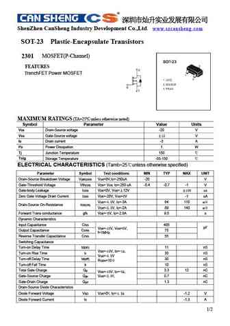
ShenZhen CanSheng Industry Development Co.,Ltd. www.szcansheng.com SOT-23 Plastic-Encapsulate Transistors 2301 MOSFET(P-Channel) FEATURES renchFET Power MOSFET T MAXIMUM RATINGS (TA=25 unless otherwise noted) Symbol Parameter Value Units VDS Drain-Source voltage -20 V VGS Gate-Source voltage 12 V ID Drain current -3 A PD Powe
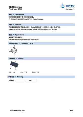
brcs2301ama.pdf
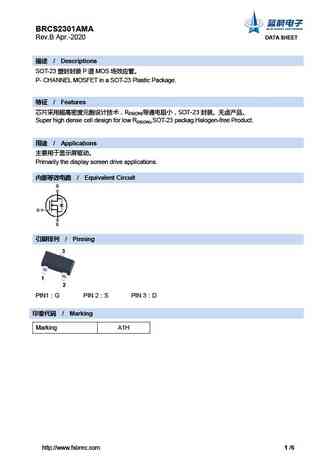
BRCS2301AMA Rev.B Apr.-2020 DATA SHEET / Descriptions SOT-23 P MOS P- CHANNEL MOSFET in a SOT-23 Plastic Package. / Features R SOT-23 DS(ON) Super high dense cell design for low RDS(ON),SOT-23 packag.Halogen-free Product. / Applications
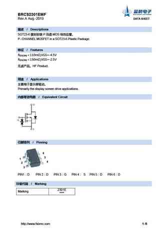
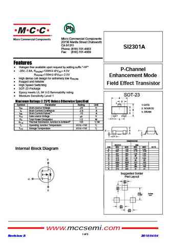
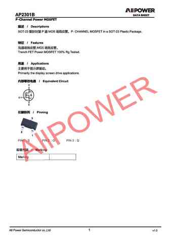
si2301.pdf
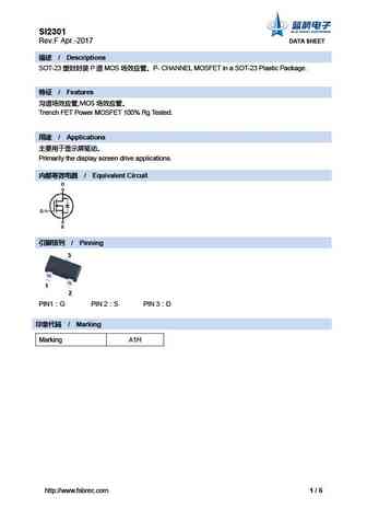
SI2301 Rev.F Apr.-2017 DATA SHEET / Descriptions SOT-23 P MOS P- CHANNEL MOSFET in a SOT-23 Plastic Package. / Features ,MOS Trench FET Power MOSFET 100% Rg Tested. / Applications Primarily the display screen drive applications. / Equivalen
lp2301alt1g.pdf
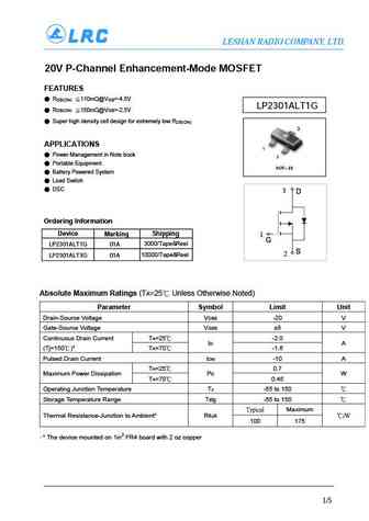
LESHAN RADIO COMPANY, LTD. 20V P-Channel Enhancement-Mode MOSFET FEATURES RDS(ON) 110m @VGS=-4.5V LP2301ALT1G RDS(ON) 150m @VGS=-2.5V Super high density cell design for extremely low RDS(ON) 3 APPLICATIONS 1 Power Management in Note book 2 Portable Equipment SOT 23 Battery Powered System Load Switch DSC 3 Ordering Inform
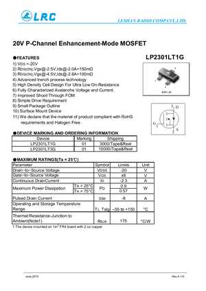
lp2301blt1g lp2301blt3g.pdf
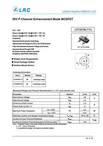
LESHAN RADIO COMPANY, LTD. 20V P-Channel Enhancement-Mode MOSFET LP2301BLT1G V = -20V DS R Vgs@-4.5V, Ids@-2.8A = 100 m DS(ON), m 3 RDS(ON), Vgs@-2.5V, Ids@-2.0A = 150 Features Advanced trench process technology 1 High Density Cell Design For Ultra Low On-Resistance 2 Fully Characterized Avalanche Voltage and Current SOT 23 (TO 236AB) Improved Shoot-Through FOM
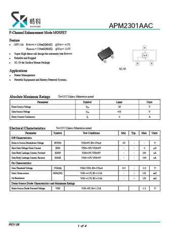
apm2301ca.pdf
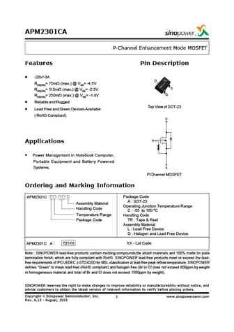
APM2301CA P-Channel Enhancement Mode MOSFET Features Pin Description -20V/-3A D RDS(ON)= 70m (max.) @ VGS= -4.5V S RDS(ON)= 115m (max.) @ VGS= -2.5V G RDS(ON)= 250m (max.) @ VGS= -1.8V Reliable and Rugged Top View of SOT-23 Lead Free and Green Devices Available ( RoHS Compliant) D G Applications Power Management in Notebook Computer, Portable Equipment and
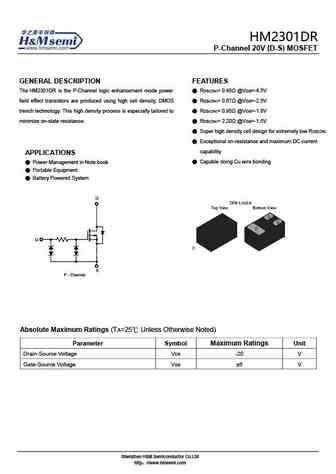
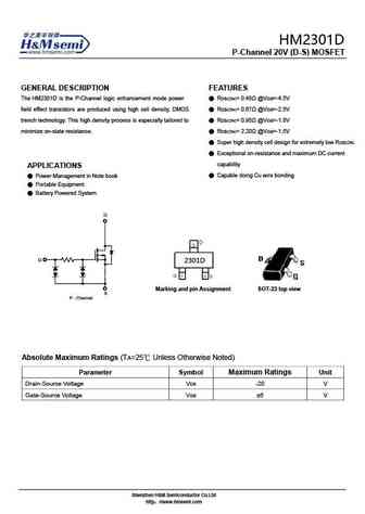
nx2301p.pdf
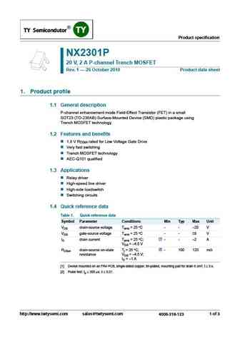
Product specification NX2301P 20 V, 2 A P-channel Trench MOSFET Rev. 1 26 October 2010 Product data sheet 1. Product profile 1.1 General description P-channel enhancement mode Field-Effect Transistor (FET) in a small SOT23 (TO-236AB) Surface-Mounted Device (SMD) plastic package using Trench MOSFET technology. 1.2 Features and benefits 1.8 V RDSon rated for Low Voltage Gate Driv
dmg2301u.pdf
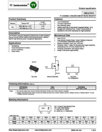
Product specification DMG2301U P-CHANNEL ENHANCEMENT MODE MOSFET Product Summary Features Low On-Resistance ID max V(BR)DSS RDS(ON) max Low Input Capacitance TA = +25 C Fast Switching Speed 80m @ VGS = 4.5V -2.7A -20V Totally Lead-Free & Fully RoHS Compliant (Notes 1 & 2) 110m @ VGS = 2.5V -2.1A Halogen and Antimony Free. Green Device (N
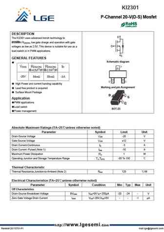
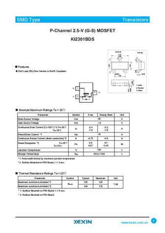
ki2301ds.pdf
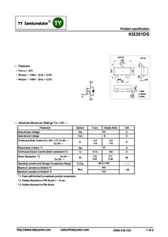
SMD Type IC SMD Type MOSFE SMD Type MOSFET SMD Type MOSFET SMD Type MOSFET Product specification KI2301 DS SOT-23 Unit mm +0.1 2.9-0.1 +0.1 0.4-0.1 3 Features VDS (V) = -20V RDS(ON) 100m (VGS = -4.5V) 1 2 +0.1 +0.05 RDS(ON) 150m (VGS = -2.5V) 0.95-0.1 0.1-0.01 +0.1 1.9-0.1 D 1.Base 1.Base 1. Gate 2.Emitter 2.Emitter 2. Source 3.
ftk2301.pdf
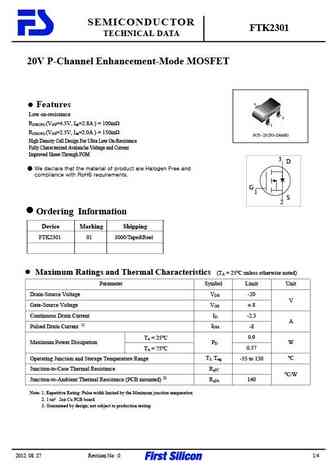
SEMICONDUCTOR FTK2301 TECHNICAL DATA 20V P-Channel Enhancement-Mode MOSFET 3 Features Low on-resistance 2 R =4.5V, I =2.8A ) = 100m DS(ON) (VGS ds 1 R =2.5V, I =2.0A ) = 150m DS(ON) (VGS ds SOT 23 (TO 236AB) High Density Cell Design For Ultra Low On-Resistance Fully Characterized Avalanche Voltage and Current Improved Shoot-Through FOM 3 D We declare that
si2301ds.pdf
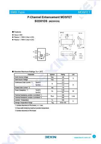
SMD Type MOSFET P-Channel Enhancement MOSFET SI2301DS (KI2301DS) Features SOT-23 Unit mm +0.1 2.9 -0.1 VDS (V) =-20V +0.1 0.4-0.1 RDS(ON) 130m (VGS =-4.5V) 3 RDS(ON) 190m (VGS =-2.5V) 1 2 +0.1 +0.05 0.95 -0.1 0.1 -0.01 +0.1 1.9 -0.1 G 1 1.Gate 3 D 2.Source S 2 3.Drain Absolute Maximum Ratings Ta = 25 Parameter Symbol Rating Unit
si2301bds-3.pdf
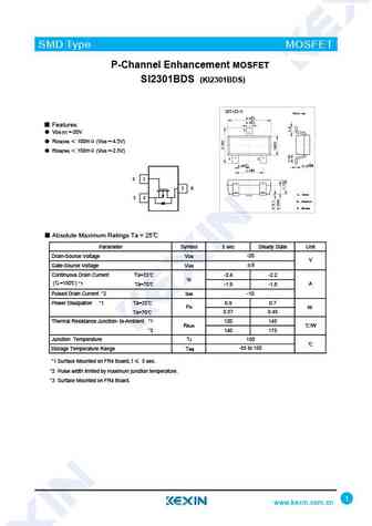
SMD Type MOSFET P-Channel Enhancement MOSFET SI2301BDS (KI2301BDS) SOT-23-3 Unit mm +0.2 2.9-0.1 +0.1 0.4 -0.1 Features 3 VDS (V) =-20V RDS(ON) 100m (VGS =-4.5V) RDS(ON) 150m (VGS =-2.5V) 1 2 +0.02 +0.1 0.15 -0.02 0.95 -0.1 +0.1 1.9 -0.2 G 1 3 D 1. Gate S 2 2. Source 3. Drain Absolute Maximum Ratings Ta = 25 Parameter Symbol 5
ki2301bds.pdf
SMD Type Transistors P-Channel 2.5-V (G-S) MOSFET KI2301BDS SOT-23 Unit mm +0.1 2.9-0.1 +0.1 0.4-0.1 3 Features 12 RoH Lead (Pb)-Free Version is RoHS Compliant. +0.1 +0.05 0.95-0.1 0.1-0.01 +0.1 1.9-0.1 1.Base 1. Gate 2.Emitter 2. Source 3. Drain 3.collector Absolute Maximum Ratings Ta = 25 Parameter Symbol 5 sec Steady State Unit Drain-Source Voltage VDS -20 V Gate-
ki2301t.pdf
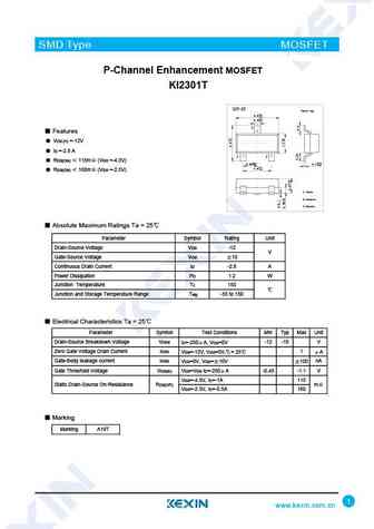
SMD Type MOSFET P-Channel Enhancement MOSFET KI2301T SOT-23 Unit mm +0.1 2.9-0.1 +0.1 0.4 -0.1 3 Features VDS (V) =-12V ID =-2.8 A 1 2 RDS(ON) 115m (VGS =-4.5V) +0.1 +0.05 0.95-0.1 0.1 -0.01 1.9+0.1 -0.1 RDS(ON) 160m (VGS =-2.5V) 1.Gate 2.Source 3.Drain Absolute Maximum Ratings Ta = 25 Parameter Symbol Rating Unit Drain-Sou
si2301ds-3.pdf

SMD Type MOSFET P-Channel Enhancement MOSFET SI2301DS (KI2301DS) SOT-23-3 Unit mm +0.2 2.9-0.1 +0.1 0.4 -0.1 Features 3 VDS (V) =-20V RDS(ON) 100m (VGS =-4.5V) RDS(ON) 150m (VGS =-2.5V) 1 2 +0.02 +0.1 0.15 -0.02 0.95 -0.1 +0.1 1.9 -0.2 G 1 3 D 1. Gate S 2 2. Source 3. Drain Absolute Maximum Ratings Ta = 25 Parameter Symbol 5 se
si2301 ki2301.pdf
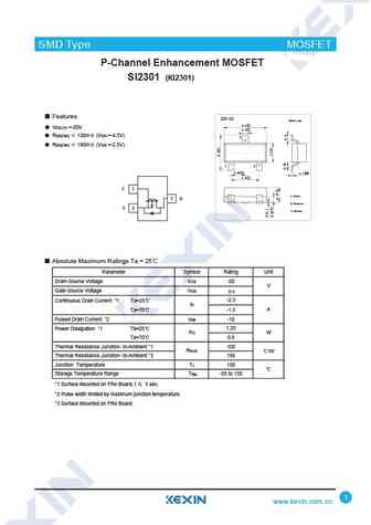
SMD Type MOSFET P-Channel Enhancement MOSFET SI2301 (KI2301) Features VDS (V) =-20V RDS(ON) 130m (VGS =-4.5V) 3 RDS(ON) 190m (VGS =-2.5V) 12 Absolute Maximum Ratings Ta = 25 Parameter Symbol Rating Unit Drain-Source Voltage VDS -20
si2301bds.pdf
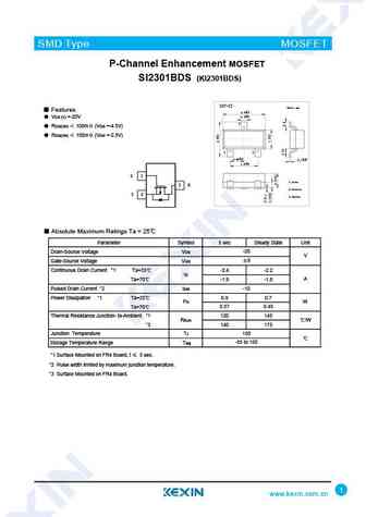
SMD Type MOSFET P-Channel Enhancement MOSFET SI2301BDS (KI2301BDS) SOT-23 Unit mm Features +0.1 2.9 -0.1 0.4+0.1 -0.1 VDS (V) =-20V 3 RDS(ON) 100m (VGS =-4.5V) RDS(ON) 150m (VGS =-2.5V) 1 2 +0.1 +0.05 0.95 -0.1 0.1-0.01 +0.1 1.9 -0.1 G 1 1.Gate 3 D 2.Source S 2 3.Drain Absolute Maximum Ratings Ta = 25 Parameter Symbol 5 sec Stea
msp2301n3.pdf
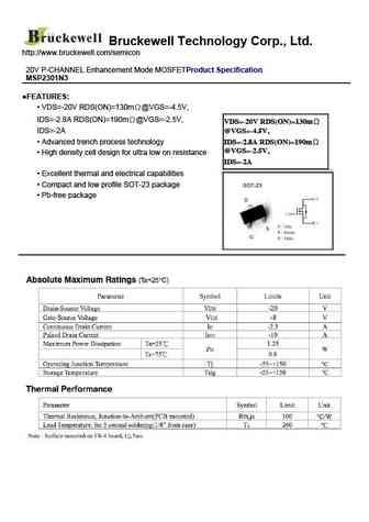
Bruckewell Technology Corp., Ltd. http //www.bruckewell.com/semicon 20V P-CHANNEL Enhancement Mode MOSFETProduct Specification MSP2301N3 FEATURES VDS=-20V RDS(ON)=130m @VGS=-4.5V, IDS=-2.8A RDS(ON)=190m @VGS=-2.5V, VDS=-20V RDS(ON)=130m @VGS=-4.5V, IDS=-2A Advanced trench process technology IDS=-2.8A RDS(ON)=190m @VGS=-2.5V, High density cell design
bws2301.pdf
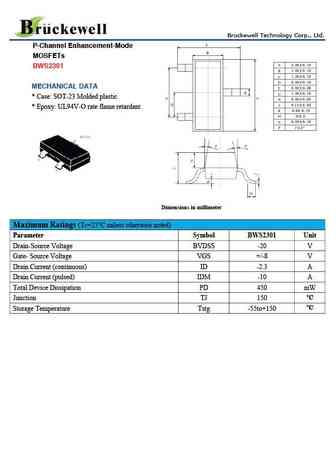
Bruckewell Technology Corp., Ltd. P-Channel Enhancement-Mode MOSFETs BWS2301 MECHANICAL DATA * Case SOT-23 Molded plastic * Epoxy UL94V-O rate flame retardant Dimensions in millimeter Maximum Ratings (Tc=25 C unless otherwise noted) Parameter Symbol BWS2301 Unit Drain-Source Voltage BVDSS -20 V Gate- Source Voltage VGS +/-8 V Drain Current (continuous) ID -2.3 A Dr
pj2301.pdf
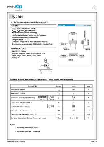
PJ2301 20V P-Channel Enhancement Mode MOSFET FEATURES RDS(ON), VGS@-1.8V,ID@-1.5A=200m RDS(ON), VGS@-4.5V,ID@-2.2A=105m 0.120(3.04) Advanced Trench Process Technology 0.110(2.80) High Density Cell Design For Ultra Low On-Resistance Specially Designed for DC/DC converters Low gate charge 0.056(1
pj2301-au.pdf
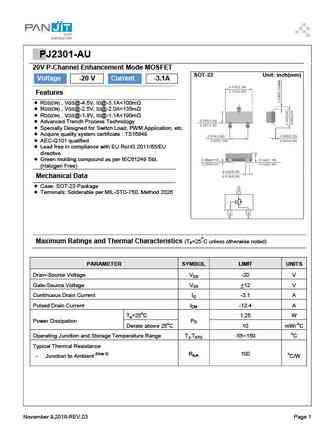
PPJ2301-AU 20V P-Channel Enhancement Mode MOSFET SOT-23 Unit inch(mm) Voltage -20 V Current -3.1A Features RDS(ON) , VGS@-4.5V, ID@-3.1A
am2301.pdf
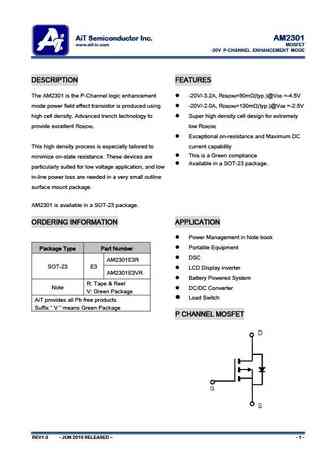
AiT Semiconductor Inc. AM2301 www.ait-ic.com MOSFET -20V P-CHANNEL ENHANCEMENT MODE DESCRIPTION FEATURES The AM2301 is the P-Channel logic enhancement -20V/-3.2A, R =90m (typ.)@V =-4.5V DS(ON) GS mode power field effect transistor is produced using -20V/-2.0A, R =130m (typ.)@V =-2.5V DS(ON) GS high cell density. Advanced trench technology to Super high density cell de
af2301p.pdf
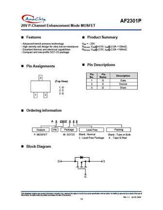
AF2301P 20V P-Channel Enhancement Mode MOSFET Features Product Summary - Advanced trench process technology VDS = - 20V - High density cell design for ultra low on-resistance RDS (on), VGS@-4.5V, IDS@-2.8A =130m . - Excellent thermal and electrical capabilities RDS (on), VGS@-2.5V, IDS@-2.0A =190m . - Compact and low profile SOT-23 package Pin Descriptions Pin Assignments
blm2301.pdf
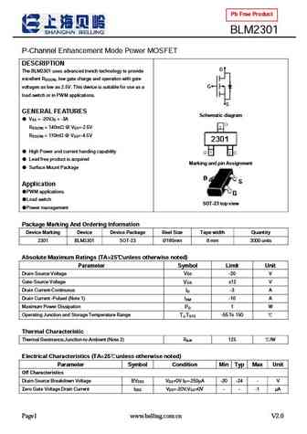
Pb Free Product BLM2301 P-Channel Enhancement Mode Power MOSFET DESCRIPTION D The BLM2301 uses advanced trench technology to provide excellent R , low gate charge and operation with gate DS(ON) G voltages as low as 2.5V. This device is suitable for use as a load switch or in PWM applications. S GENERAL FEATURES Schematic diagram V = -20V,I = -3A DS D R
chm2301esgp.pdf
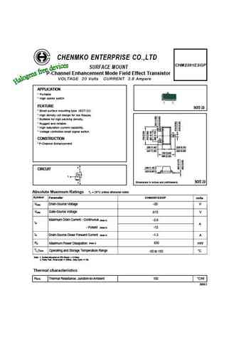
CHENMKO ENTERPRISE CO.,LTD CHM2301ESGP SURFACE MOUNT P-Channel Enhancement Mode Field Effect Transistor VOLTAGE 20 Volts CURRENT 2.8 Ampere APPLICATION * Po rtable * High speed switch FEATURE SOT-23 * Small surface mounting type. (SOT-23) * High density cell design for low RDS(ON) * Suitable for high packing density. * Rugged and reliable. (1) * High saturation current capabili
cht2301wgp.pdf
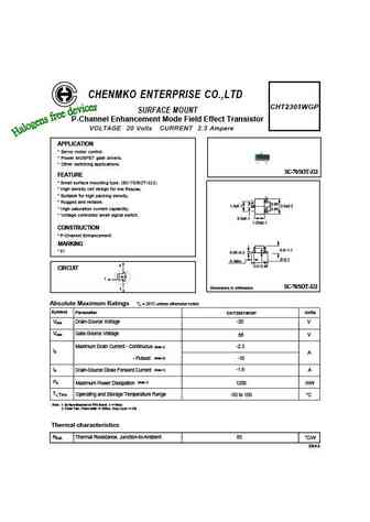
CHENMKO ENTERPRISE CO.,LTD CHT2301WGP SURFACE MOUNT P-Channel Enhancement Mode Field Effect Transistor VOLTAGE 20 Volts CURRENT 2.3 Ampere APPLICATION * Servo motor control. * Power MOSFET gate drivers. * Other switching applications. SC-70/SOT-323 FEATURE * Small surface mounting type. (SC-70/SOT-323) * High density cell design for low RDS(ON). * Suitable for high packing dens
cht2301gp.pdf
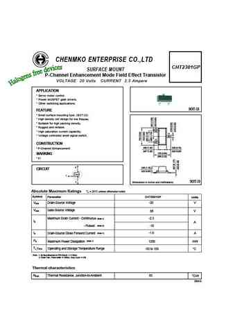
CHENMKO ENTERPRISE CO.,LTD CHT2301GP SURFACE MOUNT P-Channel Enhancement Mode Field Effect Transistor VOLTAGE 20 Volts CURRENT 2.3 Ampere APPLICATION * Servo motor control. * Power MOSFET gate drivers. * Other switching applications. SOT-23 FEATURE * Small surface mounting type. (SOT-23) * High density cell design for low RDS(ON). * Suitable for high packing density. * Rugged
cj2301-hf.pdf
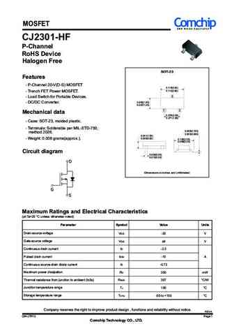
MOSFET Comchip S M D D i o d e S p e c i a l i s t CJ2301-HF P-Channel RoHS Device Halogen Free SOT-23 Features - P-Channel 20-V(D-S) MOSFET 0.118(3.00) 0.110(2.80) - Trench FET Power MOSFET. 3 - Load Switch for Portable Devices. 0.055(1.40) - DC/DC Converter. 0.047(1.20) 1 2 Mechanical data 0.079(2.00) 0.071(1.80) - Case SOT-23, molded plastic. - Terminals Solde
cpt2301.pdf
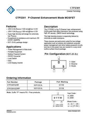
CTP2301 Crownpo Technology CTP2301 P-Channel Enhancement Mode MOSFET Features Description -20V/-2.3A,RDS(ON) =130 m @VGS=-4.5V The CTP2301 is the P-Channel logic enhancement mode power field effect transistors are produced using -20V/-1.9A,R =190 m @VGS=-2.5V DS(ON) high cell density , DMOS trench technology. Super high density cell design for extremely low RDS(ON
gsm2301as.pdf
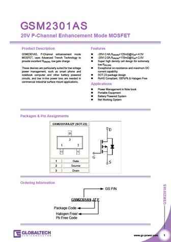
20V P-Channel Enhancement Mode MOSFET Product Description Features GSM2301AS, P-Channel enhancement mode -20V/-2.4A,RDS(ON)=125m @VGS=-4.5V MOSFET, uses Advanced Trench Technology to -20V/-2.0A,RDS(ON)=170m @VGS=-2.5V provide excellent RDS(ON), low gate charge. Super high density cell design for extremely low RDS (ON) These devices are particularly suited for low voltage
gsm2301s.pdf
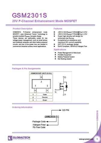
20V P-Channel Enhancement Mode MOSFET Product Description Features GSM2301S, P-Channel enhancement mode -20V/-2.8A,RDS(ON)=120m @VGS=-4.5V MOSFET, uses Advanced Trench Technology to -20V/-2.0A,RDS(ON)=170m @VGS=-2.5V provide excellent RDS(ON), low gate charge. Super high density cell design for These devices are particularly suited for low extremely low RDS (ON) volt
gsm2301a.pdf
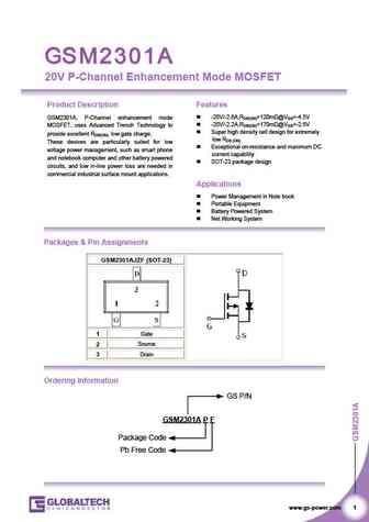
20V P-Channel Enhancement Mode MOSFET Product Description Features -20V/-2.6A,RDS(ON)=120m @VGS=-4.5V GSM2301A, P-Channel enhancement mode -20V/-2.2A,RDS(ON)=170m @VGS=-2.5V MOSFET, uses Advanced Trench Technology to Super high density cell design for extremely provide excellent RDS(ON), low gate charge. low RDS (ON) These devices are particularly suited for low
gsm2301.pdf
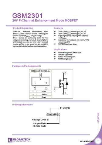
20V P-Channel Enhancement Mode MOSFET Product Description Features GSM2301, P-Channel enhancement mode -20V/-3.0A,RDS(ON)=105m @VGS=-4.5V MOSFET, uses Advanced Trench Technology to -20V/-2.4A,RDS(ON)=155m @VGS=-2.5V provide excellent RDS(ON), low gate charge. Super high density cell design for extremely These devices are particularly suited for low low RDS (ON) volta
kia2301.pdf
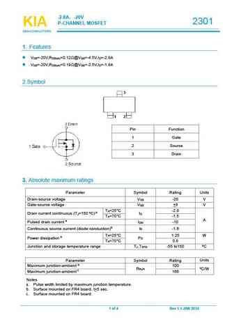
-2.8A -20V 2301 P-CHANNELMOSFET KIA KIA KIA SEMICONDUCTORS SEMICONDUCTORS SEMICONDUCTORS 1. Features V =-20V,R =0.12 @V =-4.5V,I =-2.8A DS DS(on) GS D V =-20V,R =0.19 @V =-2.5V,I =-1.8A DS DS(on) GS D 2.Symbol Pin Function 1 Gate 2 Source 3 Drain 3. Absolute maximumratings Parameter Symbol Rating Units Drain-source voltage V -20 V DS Gate-source voltage V +8 V GS
me2301a me2301a-g.pdf
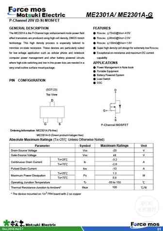
ME2301A/ ME2301A-G P-Channel 20V (D-S) MOSFET GENERAL DESCRIPTION FEATURES The ME2301A is the P-Channel logic enhancement mode power field RDS(ON) 75m @VGS=-4.5V effect transistors are produced using high cell density, DMOS trench RDS(ON) 95m @VGS=-2.5V technology. This high density process is especially tailored to RDS(ON) 130m @VGS=-1.8V minimize on-stat
me2301 me2301-g.pdf
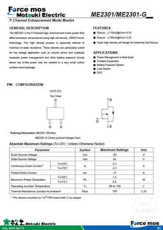
ME2301/ME2301-G P-Channel Enhancement Mode Mosfet GENERAL DESCRIPTION FEATURES RDS(ON) 110m @VGS=-4.5V The ME2301 is the P-Channel logic enhancement mode power field RDS(ON) 150m @VGS=-2.5V effect transistors are produced using high cell density , DMOS trench Super high density cell design for extremely low RDS(ON) technology. This high density process is es
me2301dc me2301dc-g.pdf
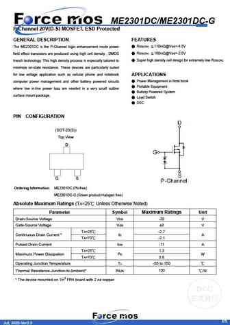
ME2301DC/ME2301DC-G P-Channel 20V(D-S) MOSFET, ESD Protected GENERAL DESCRIPTION FEATURES The ME2301DC is the P-Channel logic enhancement mode power RDS(ON) 110m @VGS=-4.5V field effect transistors are produced using high cell density , DMOS RDS(ON) 150m @VGS=-2.5V trench technology. This high density process is especially tailored to Super high density cell design
me2301gc me2301gc-g.pdf
ME2301GC/ ME2301GC-G P-Channel 20V (D-S) MOSFET GENERAL DESCRIPTION FEATURES RDS(ON) 75m @VGS=-4.5V The ME2301GC is the P-Channel logic enhancement mode power RDS(ON) 95m @VGS=-2.5V field effect transistors are produced using high cell density, DMOS RDS(ON) 130m @VGS=-1.8V trench technology. This high density process is especially tailored to Sup
me2301dn me2301dn-g.pdf
ME2301DN/ME2301DN-G P-Channel 20V(D-S) MOSFET, ESD Protected GENERAL DESCRIPTION FEATURES The ME2301DN is the P-Channel logic enhancement mode power RDS(ON) 90m @VGS=-4.5V field effect transistors are produced using high cell density , DMOS RDS(ON) 130m @VGS=-2.5V trench technology. This high density process is especially tailored to Super high density cell desig
me2301s me2301s-g.pdf
ME2301S/ME2301S-G P-Channel 20V (D-S) MOSFET GENERAL DESCRIPTION FEATURES RDS(ON) 110m @VGS=-4.5V The ME2301S is the P-Channel logic enhancement mode power field RDS(ON) 150m @VGS=-2.5V effect transistors are produced using high cell density , DMOS trench Super high density cell design for extremely low RDS(ON) technology. This high density process is espec
mmp2301.pdf
MMP2301 Data Sheet M-MOS Semiconductor Hong Kong Limited 20V P-Channel Enhancement-Mode MOSFET VDS= -20V RDS(ON), Vgs@-4.5V, Ids@-2.8A = 100m RDS(ON), Vgs@-2.5V, Ids@-2.0A = 150m RDS(ON), Vgs@-1.8V, Ids@-2.0A = 170m Features Advanced trench process technology High Density Cell Design For Ultra Low On-Resistance SOT- 23 Internal Schematic Diagram Top View P-Channel MOSFET M
nce2301a.pdf
Pb Free Product http //www.ncepower.com NCE2301A NCE P-Channel Enhancement Mode Power MOSFET Description The NCE2301A uses advanced trench technology to provide excellent RDS(ON), low gate charge and operation with gate voltages as low as 2.5V. This device is suitable for use as a load switch or in PWM applications. General Features VDS = -15V,ID = -3.0A Schematic diagram
nce2301c.pdf

Pb Free Product http //www.ncepower.com NCE2301C NCE P-Channel Enhancement Mode Power MOSFET Description D The NCE2301C uses advanced trench technology to provide excellent RDS(ON), low gate charge and operation with gate G voltages as low as 1.8V. This device is suitable for use as a load switch or in PWM applications. S General Features Schematic diagram VDS = -15V,
nce2301e.pdf
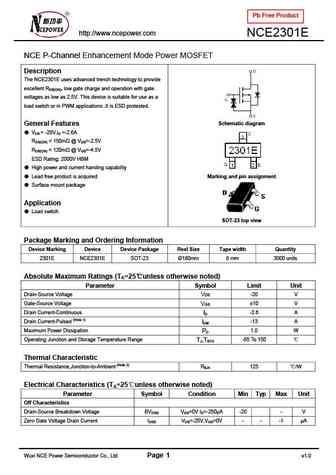
Pb Free Product http //www.ncepower.com NCE2301E NCE P-Channel Enhancement Mode Power MOSFET Description The NCE2301E uses advanced trench technology to provide excellent RDS(ON), low gate charge and operation with gate voltages as low as 2.5V. This device is suitable for use as a load switch or in PWM applications .It is ESD protested. Schematic diagram General Features
ncea2301.pdf
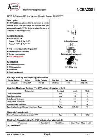
http //www.ncepower.com NCEA2301 NCE P-Channel Enhancement Mode Power MOSFET Description The NCEA2301 uses advanced trench technology to provide excellent R , low gate charge and operation with gate DS(ON) voltages as low as 2.5V. This device is suitable for use as a load switch or in PWM applications. General Features V = -20V,I = -3A DS D R
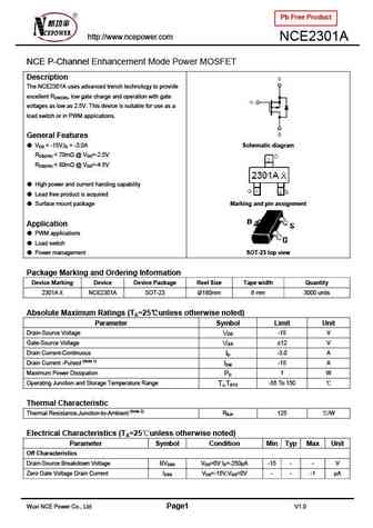
nce2301.pdf
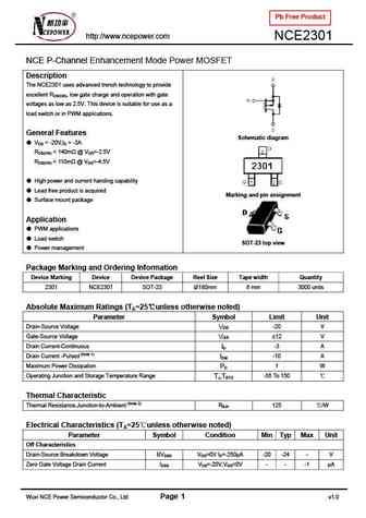
Pb Free Product http //www.ncepower.com NCE2301 NCE P-Channel Enhancement Mode Power MOSFET Description The NCE2301 uses advanced trench technology to provide excellent RDS(ON), low gate charge and operation with gate voltages as low as 2.5V. This device is suitable for use as a load switch or in PWM applications. General Features Schematic diagram VDS = -20V,ID = -3A
nce2301f.pdf
Pb Free Product http //www.ncepower.com NCE2301F NCE P-Channel Enhancement Mode Power MOSFET Description D The NCE2301F uses advanced trench technology to provide excellent RDS(ON), low gate charge and operation with gate G voltages as low as 1.8V. This device is suitable for use as a load switch or in PWM applications. S General Features Schematic diagram VDS = -20V,
nce2301d.pdf

Pb Free Product http //www.ncepower.com NCE2301D NCE P-Channel Enhancement Mode Power MOSFET Description D The NCE2301D uses advanced trench technology to provide excellent RDS(ON), low gate charge and operation with gate G voltages as low as 1.8V. This device is suitable for use as a load switch or in PWM applications. S General Features Schematic diagram VDS = -20V,
nce2301b.pdf

Pb Free Product http //www.ncepower.com NCE2301B NCE P-Channel Enhancement Mode Power MOSFET Description D The NCE2301B uses advanced trench technology to provide excellent RDS(ON), low gate charge and operation with gate G voltages as low as 1.8V. This device is suitable for use as a load switch or in PWM applications. S General Features Schematic diagram VDS = -20V,
stp2301.pdf
STP2301 -20V P-Channel Enhancement Mode MOSFET DESCRIPTION FEATURE The STP2301 is the P-Channel logic enhancement -20V/-3.0A, RDS(ON) =80m (typ.)@VGS =-4.5V mode power field effect transistor is produced using -20V/-2.0A, RDS(ON) =105m (typ.)@VGS =-2.5V high cell density. advanced trench technology to provide excellent RDS(ON). .low gate charge and Super h
ssm2301gn.pdf
SSM2301N P-CHANNEL ENHANCEMENT-MODE POWER MOSFET Simple drive requirement BV -20V DSS Small package outline RDS(ON) 130m D Surface-mount device ID -2.3A S SOT-23 G Description D Power MOSFETs from Silicon Standard Corp. provide the designer with the best combination of fast switching, low G on-resistance and cost-effectiveness. S The SOT-23 package is widely preferred for co
sl2301.pdf
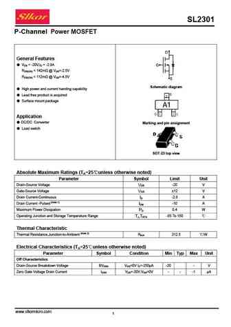
SL2301 P-Channel Power MOSFET D General Features VDS = -20V,ID = -2.8A G RDS(ON)
sl2301s.pdf
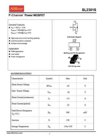
SL2301S SOT-23 Package Information Dimensions in Millimeters Symbol MIN. MAX. A 0.900 1.150 A1 0.000 0.100 A2 0.900 1.050 b 0.300 0.500 c 0.080 0.150 D 2.800 3.000 E 1.200 1.400 E1 2.250 2.550 e 0.950TYP e1 1.800 2.000 L 0.550REF L1 0.300 0.500 0 8 www.slkormicro.com 3
st2301a.pdf
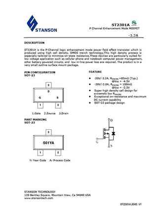
ST2301A P Channel Enhancement Mode MOSFET -3.2A DESCRIPTION ST2301A is the P-Channel logic enhancement mode power field effect transistor which is produced using high cell density, DMOS trench technology.This high density process is especially tailored to minimize on-state resistance.These devices are particularly suited for low voltage application such as cellular phone and not
tp2301pr.pdf
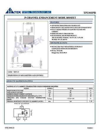
TP2301PR P-CHANNEL ENHANCEMENT-MODE MOSFET FEATURES ADVANCED TRENCH PROCESS TECHNOLOGY HIGH DENSITY CELL DESIGN FOR ULTRA LOW ON-RESISTANCE FULLY CHARACTERIZED AVALANCHE VOLTAGE AND CURRENT IMPROVED SHOOT-THROUGH FOM BOTH NORMAL AND PB FREE PRODUCT ARE AVAILABLE NORMAL 80 95% SN, 5 20% PB PB FREE 99% SN ABOVE MECHANICAL DATA WE DECLARE THAT
si2301a.pdf
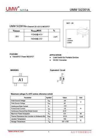
R UMW UMW SI2301A SOT 23 UMW SI2301A P-Channel 20-V(D-S) MOSFET ID V(BR)DSS RDS(on)MAX 112m @-4.5V -20V A -2.8 1. GATE 142m @-2.5V 2. SOURCE 3. DRAIN FEATURE APPLICATION TrenchFET Power MOSFET z z Load Switch for Portable Devices z DC/DC Converter MARKING Equivalent Circuit A1 Maximum ratings (Ta=25 unless otherwise noted) Parameter Symbol Valu
si2301b.pdf
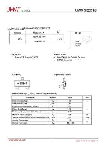
R UMW UMW SI2301B UMW SI2301B UMW SI2301B P-Channel 20-V(D-S) MOSFET UMW SI2301B ID V(BR)DSS RDS(on)MAX SOT-23 120 m @-4.5V -20V 2.5 A m @-2.5V 150 1. GATE 2. SOURCE 3. DRAIN APPLICATION FEATURE z Load Switch for Portable Devices TrenchFET Power MOSFET z DC/DC Converter MARKING Equivalent Circuit A1SHB Maximum ratings (Ta=25 unless otherwise note
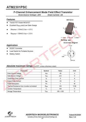
atm2301psc.pdf
ATM2301PSC P-Channel Enhancement Mode Field Effect Transistor Drain-Source Voltage -20V Drain Current -3A Features Trench FET Power MOSFET Excellent R and Low Gate Charge DS(on) R
atm2301psa.pdf
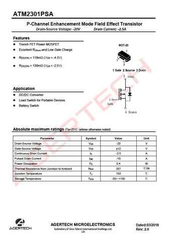
ATM2301PSA P-Channel Enhancement Mode Field Effect Transistor Drain-Source Voltage -20V Drain Current -2.5A Features Trench FET Power MOSFET Excellent R and Low Gate Charge DS(on) R
ap2301.pdf
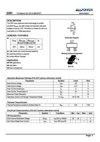
2301 P-Channel 20-V(D-S) MOSFET DATA SHEET DESCRIPTION D The 2301 uses advanced trench technology to provide excellent RDS(ON), low gate charge and operation with gate G voltages as low as 2.5V. This device is suitable for use as a load switch or in PWM applications. S GENERAL FEATURES Schematic diagram VDSS RDS(ON) RDS(ON) ID (Typ) @-2.5V @-4.5V (Typ) -20V 64m
as2301.pdf
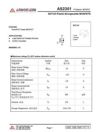
AS2301 P-Channel MOSFET SOT-23 Plastic-Encapsulate MOSFETS SOT-23 FEATURE TrenchFET Power MOSFET 1. GATE APPLICATIONS 2. SOURCE Load Switch for Portable Devices 3. DRAIN DC/DC Converter MARKING A1 Maximum ratings (Ta=25 unless otherwise noted) Characteristic Symbol Max Unit Drain-Source Voltage BVDSS -20 V -
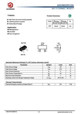
asdm2301.pdf
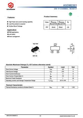
ASDM2301 20V P-CHANNEL MOSFET Product Summary Features High Power and current handing capability VDSS RDS(ON) RDS(ON) ID (Typ) (Typ) @-4.5V @-2.5V Lead free product is acquired Surface Mount Package -20V 65m 83m -3 A Application PWM applications Load switch Power management top view D G SOT-23 Absolute Maximum Ratings (TA=25 unless otherwi
asdm2301za.pdf
ASDM2301ZA 20V P-CHANNEL MOSFET Features Product Summary High Power and current handing capability VDSS RDS(ON) RDS(ON) ID Lead free product is acquired (Typ) (Typ) @-4.5V @-2.5V Surface Mount Package -20V 65m 83m -3 A Application PWM applications Load switch Power management top view D G SOT-23 Absolute Maximum Ratings (TA=25 unless other
si2301-p.pdf
SI2301-P MOSFET ROHS P-Channel MOSFET SOT-23 - Features Advanced trench process technology High Density Cell Design For Ultra Low On-Resistance Maximum Ratings & Thermal Characteristics (Ratings at 25 ambient temperature unless otherwise specified.) Parameter Symbol Limit Unit Drain-Source Voltage VDS -20 V Gate-Source Voltage 10 VGS ID Continuous Drain
si2301s.pdf
SI2301S MOSFET ROHS P-Channel Enhancement-Mode MOSFET SOT-23 - Features Low RDS(on) @VGS=-4.5V -3.3V Logic Level Control P Channel SOT23 Package Pb-Free, RoHS Compliant Applications V R Typ I Max (BR)DSS DS(ON) D High-side Load Switch 125m @ 4.5V Switching Circuits -20V -2.3A High Speed line Driver 140m @ 3.3V Order Information
si2301f.pdf
SI2301F P-Channel MOSFET Features Pin Configurations V = -20V DS I D = -2.2A R @V = -4.5V, Typ =95m DS(ON) GS R @V = -2.5V, Typ =130m DS(ON) GS General Description Advanced trench process technology High power and current handing capability Lead free product is acquired SOT-23 for Surface Mount Package. Application PWM applications Lo
bmdfn2301.pdf
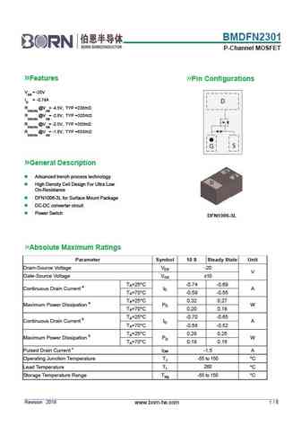
BMDFN2301 P-Channel MOSFET Features Pin Configurations V = -20V DS I D = -0.74A D R @V = -4.5V, TYP =230m DS(ON) GS R @V = -2.8V, TYP =320m DS(ON) GS R @V = -2.5V, TYP =355m DS(ON) GS R @V = -1.8V, TYP =650m DS(ON) GS S G General Description G Advanced trench process technology S D High Density Cell Design For Ultra Low On-Resistance
bms2301.pdf
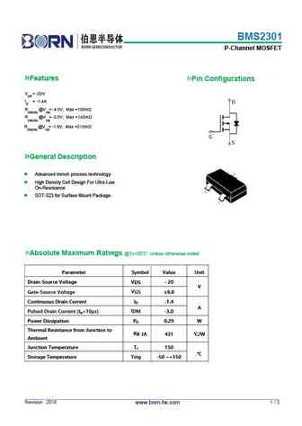
BMS2301 P-Channel MOSFET Features Pin Configurations V = -20V DS I D = -1.4A R @V = -4.5V, Max =100m DS(ON) GS R @V = -2.5V, Max =140m DS(ON) GS R @V = -1.8V, Max =210m DS(ON) GS General Description Advanced trench process technology High Density Cell Design For Ultra Low On-Resistance SOT-323 for Surface Mount Package. Absolute Maximum Ratings
fs2301.pdf
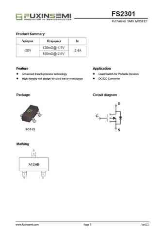
FS2301 P-Channel SMD MOSFET Product Summary V R I (BR)DSS DS(on)MAX D 120m @-4.5V -20V -2.4A 180m @-2.5V Feature Application Advanced trench process technology Load Switch for Portable Devices High density cell design for ultra low on-resistance DC/DC Converter Package Circuit diagram D G SOT-23 S Marking A1SHB www.fuxinsemi.com Page 1 Ver2.1 FS2301 P-Ch
en2301.pdf
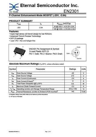
Eternal Semiconductor Inc. EN2301 P-Channel Enhancement-Mode MOSFET (-20V, -2.8A) PRODUCT SUMMARY VDSS ID RDS(on) (m )Typ. 85 @ VGS = -4.5V,ID=-2.8A -20V -2.8A 105 @ VGS = -2.5V,ID=-2.0A Features Super high dense cell trench design for low RDS(on) Advanced Trench Process Technology SOT-23 package Lead Pb -free and halogen-free EN2301 Pin Assignment & Symbol


as2301.pdf
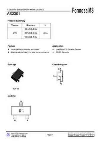
P-Channel Enhancement Mode MOSFET Formosa MS AS2301 Product Summary V(BR)DSS RDS(on)MAX ID 64m @-4.5V -20V 80m @-2.5V -3.4A 95m @-1.8V Feature Application Advanced trench process technology Load Switch for Portable Devices High density cell design for ultra low on-resistance DC/DC Converter Package Circuit diagram SOT-23 Marking S1. Document ID http //www.form
gp2301.pdf
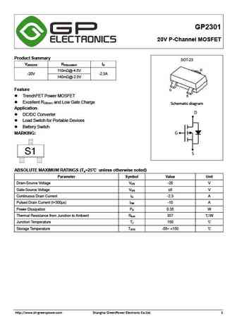
GP2301 20V P-Channel MOSFET Product Summary SOT-23 V R I (BR)DSS DS(on)MAX D 110m @-4.5V -20V -2.3A 140m @-2.5V Feature TrenchFET Power MOSFET Excellent RDS(on) and Low Gate Charge Schematic diagram Application DC/DC Converter Load Switch for Portable Devices Battery Switch MARKING ABSOLUTE MAXIMUM RATINGS (Ta=25 unless otherwise note
si2301.pdf
Plastic-Encapsulate Mosfets FEATURES SI2301 P-Channel MOSFET High dense cell design for extremely low RDS(ON) Rugged and reliable Case Material Molded Plastic. Absolute Maximum Ratings (TA=25oC, unless otherwise noted) Parameter Symbol Ratings Units Drain-Source Voltage VDS -20 V 1.Gate Gate-Source Voltage VGS 8 V 2.Source SOT-23 Drain Current (Continuous) ID -2.3 A 3.Drain 1 D
hss2301c.pdf
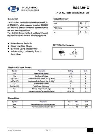
HSS2301C P-Ch 20V Fast Switching MOSFETs Description Product Summary The HSS2301C is the high cell density trenched P- V -20 V DS ch MOSFETs, which provides excellent RDSON and efficiency for most of the small power switching R 130 m DS(ON),typ and load switch applications. I -2 A D The HSS2301C meet the RoHS and Green Product requirement with full function reliability a
hss2301b.pdf
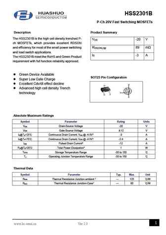
HSS2301B P-Ch 20V Fast Switching MOSFETs Description Product Summary The HSS2301B is the high cell density trenched P- V -20 V DS ch MOSFETs, which provides excellent RDSON and efficiency for most of the small power switching R 89 m DS(ON),typ and load switch applications. I -3 A D The HSS2301B meet the RoHS and Green Product requirement with full function reliability ap
hx2301.pdf
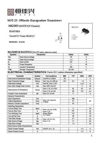
SOT-23 -3Plastic-Encapsulate Transistors HX2301 MOSFET(P-Channel) FEATURES TrenchFET Power MOSFET MARKING A1SHB MAXIMUM RATINGS (TA=25 unless otherwise noted) Symbol Parameter Value Units VDS Drain-Source voltage -20 V VGS Gate-Source voltage 12 V -2.8 A ID Drain current PD Power Dissipation 1 W Tj Junction Temperature 150 Tstg Storage Temperature -55-150 E
hx2301a.pdf
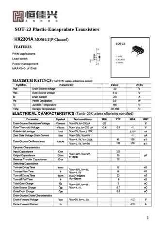
SOT-23 Plastic-Encapsulate Transistors HX2301A MOSFET(P-Channel) FEATURES PWM applications Load switch Power management MARKING A1SHB MAXIMUM RATINGS (TA=25 unless otherwise noted) Symbol Parameter Value Units VDS Drain-Source voltage -20 V VGS Gate-Source voltage 12 V ID Drain current -2.5 A PD Power Dissipation 0.9 W Tj Junction Temperature 150 Tstg Storage Temperature
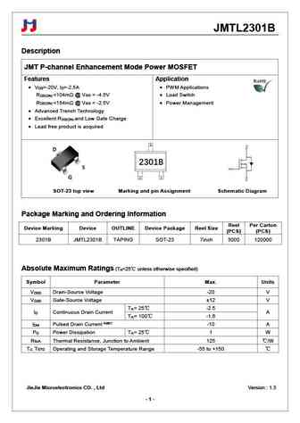
jmtl2301b.pdf
JMTL2301B Description JMT P-channel Enhancement Mode Power MOSFET Features Application V =-20V, I =-2.5A PWM Applications DS D R
jmtl2301e.pdf
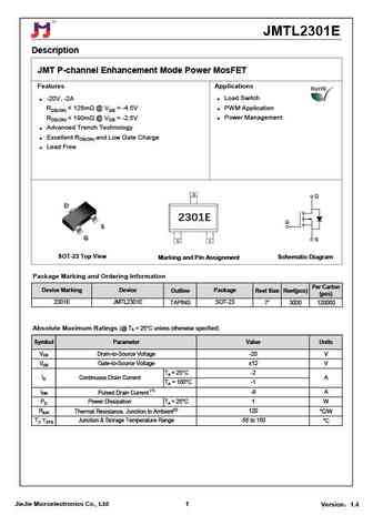
JMTL2301E Description JMT P-channel Enhancement Mode Power MosFET Features Applications -20V, -2A Load Switch RDS(ON)
jmtl2301c.pdf
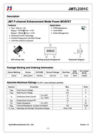
JMTL2301C Description JMT P-channel Enhancement Mode Power MOSFET Features Application V = -20V, I = -3A PWM Applications DS D R
jst2301h.pdf
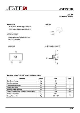
JST2301H -20V,-3A P-Channel Mosfet FEATURES SOT-23 RDS(ON) 110m @VGS=-4.5V RDS(ON) 140m @VGS=-2.5V APPLICATIONS Load Switch for Portable Devices DC/DC Converter MARKING P-CHANNEL MOSFET Maximum ratings (Ta=25 unless otherwise noted) Parameter Symbol Value Unit Drain-Source Voltage VDS -20 V Gate-Source Voltage V 12 GS I -3 D Continuous Drain Current A Pulse
jsm2301s.pdf
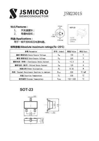
JSM2301S /Features 1 2 /Applications /Absolute maximum ratings(Ta=25 ) /Parameter / Symbol /Value /Unit - /Drain-Source Voltage V -20 V DS - /Gate-Source Voltage V 8 V GS /C
lpm2301b3f.pdf
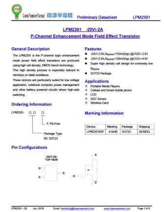
Preliminary Datasheet LPM2301 LPM2301 -20V/-2A P-Channel Enhancement Mode Field Effect Transistor General Description Features -20V/-2.0A,RDS(ON)=170m (typ.)@VGS=-2.5V The LPM2301 is the P-channel logic enhancement -20V/-2.0A,RDS(ON)=130m (typ.)@VGS=-4.5V mode power field effect transistors are produced Super high density cell design for extremely low using high
lpsc2301.pdf
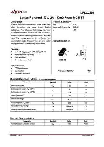
LPSC2301 Lonten P-channel -20V, -2A, 110m Power MOSFET Description Product Summary These P-Channel enhancement mode power field VDSS -20V effect transistors are using trench DMOS RDS(on).max@ VGS=-4.5V 110m technology. This advanced technology has been ID -2A especially tailored to minimize on-state resistance, provide superior switching performance, and with stand high ener
np2301amr-g.pdf
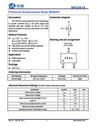
NP2301A P-Channel Enhancement Mode MOSFET Description Schematic diagram The NP2301A uses advanced trench technology S to provide excellent RDS(ON), low gate charge and operation with gate voltages as low as 1.8V. This device is suitable for use as a load switch or in PWM G applications. General Features D VDS =-20V ID =-2.8A Marking and pin assignment RDS(ON)(Typ.)=7
si2301s.pdf
SI2301S SOT-23 Plastic-Encapsulate MOSFETS SOT-23 20V P-Channel MOSFET 3 ID Max V(BR)DSS RDS(on)Typ 125m @4.5V 1. GATE -2.3A -20V 2. SOURCE 140m @3.3V 1 3. DRAIN 2 APPLICATION Features Load Switch for Portable Devices Trench FET Power MOSFET DC/DC Converter MARKING Equivalent circuit D A1sHB G S PACKAGE SPECIFICATIONS Reel DIA. Q'TY/Ree
si2301.pdf
SI2301 SOT-23 Plastic-Encapsulate MOSFETS SOT-23 20V P-Channel MOSFET 3 ID Max V(BR)DSS RDS(on)Typ 70m @4.5V 1. GATE -3.0A -20V 2. SOURCE 78m @3.3V 1 3. DRAIN 2 APPLICATION Features Load Switch for Portable Devices Trench FET Power MOSFET DC/DC Converter MARKING Equivalent circuit D A1sHB G S PACKAGE SPECIFICATIONS Reel DIA. Q'TY/Reel
si2301ai-ms.pdf
www.msksemi.com SI2301AI-MS Semiconductor Compiance General Features V = -20V,I = -3A DS D R
mem2301xg-n.pdf
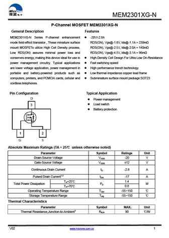
MEM2301XG-N P-Channel MOSFET MEM2301XG-N General Description Features MEM2301XG-N Series P-channel enhancement -20V/-2.8A mode field-effect transistor , These miniature surface RDS(ON), Vgs@-1.8V, Ids@-1.1A = 230m mount MOSFETs utilize High Cell Density process. RDS(ON), Vgs@-2.5V, Ids@-2.0A = 140m Low RDS(ON) assures minimal power loss and RDS(ON), Vgs@-4.5V, Ids@-3.1A = 9
mem2301x.pdf
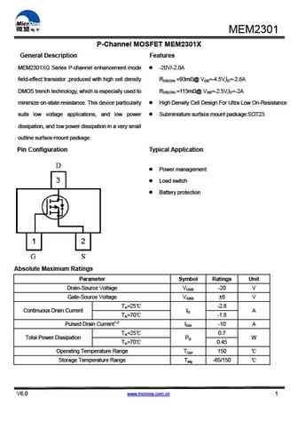
MEM2301 P-Channel MOSFET MEM2301X General Description Features MEM2301XG Series P-channel enhancement mode -20V/-2.8A field-effect transistor ,produced with high cell density RDS(ON) =93m @ VGS=-4.5V,ID=-2.8A DMOS trench technology, which is especially used to RDS(ON) =113m @ VGS=-2.5V,ID=-2A minimize on-state resistance. This device particularly High Density Cell Design
si2301a.pdf
SOT-23 Plastic-Encapsulate MOSFETS SI2301A SI2301A P-Channel 20-V(D-S) MOSFET V(BR)DSS RDS(on)MAX ID SOT-23 0.085 @-4.5V -20V -3.0A 3 0.110 @-2.5V 1.GATE 2.SOURCE 3.DRAIN 1 2 General FEATURE TrenchFET Power MOSFET MARKING Equivalent Circuit Lead free product is acquired Surface mount package A1 w APPLICATION Load Switch for Portable Devices DC/DC Converter
si2301.pdf

SOT-23 Plastic-Encapsulate MOSFETS SI2301 SI2301 P-Channel 20-V(D-S) MOSFET V(BR)DSS RDS(on)MAX ID SOT-23 0.100 @-4.5V -20V -2.8A 3 0.130 @-2.5V 1.GATE 2.SOURCE 3.DRAIN 1 2 General FEATURE TrenchFET Power MOSFET MARKING Equivalent Circuit Lead free product is acquired Surface mount package - A1sHB w APPLICATION Load Switch for Portable Devices DC/DC Conv
pjm2301psa-s.pdf
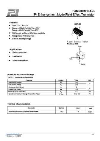
PJM2301PSA-S P- Enhancement Mode Field Effect Transistor Features SOT-23 VDS= -20V I = -2A D R =120m (typ) @ V =-2.5V DS(ON) GS R =88m (typ) @ V =-4.5V DS(ON) GS High power and current handing capability Halogen and Antimony Free Surface mount package 1. Gate 2.Source 3.Drain Marking S01 Drain 3 Applications Battery protection Load s
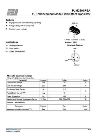
2301p.pdf
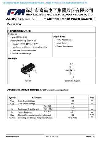
FM , FM WWW.SZLCSC.COM, SHEN ZHEN FINE MADE ELECTRONICS GROUP CO., LTD. 2301P( S&CIC1974) P-Channel Trench Power MOSFET Description P-channel MOSFET Features Application V =-20V, I =-2.8A D
si2301a.pdf
SI2301A 20V P-Channel Enhancement-Mode MOSFET VDS= -20V RDS(ON), Vgs@-4.5V, Ids@-3.0A 110m RDS(ON), Vgs@-2.5V, Ids@-2.0A 140m Features Advanced trench process technology High Density Cell Design For Ultra Low On-Resistance Package Dimensions D G S SOT-23(PACKAGE) Millimeter Millimeter REF. REF. Min. Max. Min. Max. A 2.70 3.10 G 1.90 REF. B 2.40 2.80 H 1.00 1.3
si2301.pdf
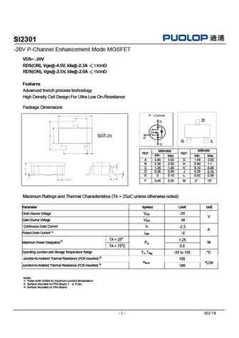
SI2301 -20V P-Channel Enhancement Mode MOSFET VDS= -20V RDS(ON), Vgs@-4.5V, Ids@-2.3A 130m RDS(ON), Vgs@-2.5V, Ids@-2.0A 190m Features Advanced trench process technology High Density Cell Design For Ultra Low On-Resistance Package Dimensions D SOT-23 G S Millimeter Millimeter REF. REF. Min. Max. Min. Max. A 2.80 3.00 G 1.80 2.00 B 2.30 2.50 H 0.90 1.1 C 1.20
apm2301aac.pdf
APM2301AAC P-Channel Enhancement Mode MOSFET Feature DS(ON) GS -20V/-3A R = 120m (MAX) @V = -4.5V. DS(ON) GS R = 150m (MAX) @V = -2.5V. DS(ON) Super High dense cell design for extremely low R Reliable and Rugged SC-59 for Surface Mount Package SC-59 Applications Power Management Portable Equipment and Battery Powered Systems. A T =25 U
wtm2301.pdf
WTM2301 P-Channel Enhancement Mode Power MOSFET Description The WTM2301 uses advanced trench technology to provide excellent R , low gate charge and operation with gate DS(ON) voltages as low as 2.5V. This device is suitable for use as a battery protection or in other switching application. Features V DS = -20V, lD = -3A R
si2301.pdf
SI2301 SOT-23 (SOT-23 Field Effect Transistors) P-Channel Enhancement-Mode MOS FETs P MOS MAXIMUM RATINGS Characteristic Symbol Max Unit Drain-Source Voltage -20 V BV DSS - Gate- Source Voltage +10 V V GS - Drain Current (continuous) I -2.2
si2301.pdf
SHENZHEN LONG JING MICRO-ELECTRONICS CO., LTD. SOT-23 Plastic-Encapsulate MOSFETS SI2301 P-Channel 20V(D-S) MOSFET Features V = -20V, I = -2.5A DS D R
tf2301a.pdf
SHENZHEN TUOFENG SEMICONDUCTOR TECHNOLOGY CO.,LTD SOT-23 Plastic-Encapsulate MOSFETS TF2301A TF2301A P-Channel 20-V(D-S) MOSFET V(BR)DSS RDS(on)MAX ID SOT-23 0.085 @-4.5V -20V -3.0A 3 0.110 @-2.5V 1.GATE 2.SOURCE 3.DRAIN 1 2 General FEATURE TrenchFET Power MOSFET MARKING Equivalent Circuit Lead free product is acquired Surface mount package A1 w APPLICATION L
tf2301.pdf

SHENZHEN TUOFENG SEMICONDUCTOR TECHNOLOGY CO.,LTD SOT-23 Plastic-Encapsulate MOSFETS TF2301 TF2301 P-Channel 20-V(D-S) MOSFET V(BR)DSS RDS(on)MAX ID SOT-23 0.100 @-4.5V -20V -2.8A 3 0.130 @-2.5V 1.GATE 2.SOURCE 3.DRAIN 1 2 General FEATURE TrenchFET Power MOSFET MARKING Equivalent Circuit Lead free product is acquired Surface mount package - A1sHB w APPLICATION
si2301.pdf
SI2301 SI2305 AO3401 SOT-23 Plastic-Encapsulate MOSFETS P-Channel 20-V( D-S) MOSFET FEATURE TrenchFET Power MOSFET APPLICATIONS z Load Switch for Portable Devices z DC/DC Converter MARKING Equivalent Circuit A1SHB A09T A19T 1.GATE 2.SOURCE 3.DRAIN Maximum ratings (Ta=25 unless otherwise noted) Parameter Symbol Value Unit Drain-Source Voltage VDS -20 V Gate-Sourc
wst2301.pdf
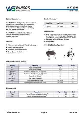
WST2301 P-Ch MOSFET General Description Product Summery The WST2301 is the highest performance trench BVDSS RDSON ID P-ch MOSFET with extreme high cell density , which provide excellent RDSON and gate -20V 100m -2.9A charge for most of the small power switching and load switch applications. Applications The WST2301 meet the RoHS and Green Product requirement with full fu
wst2301a.pdf
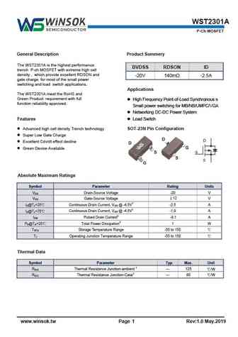
WST2301A P-Ch MOSFET General Description Product Summery The WST2301A is the highest performance BVDSS RDSON ID trench P-ch MOSFET with extreme high cell density , which provide excellent RDSON and -20V 140m -2.5A gate charge for most of the small power switching and load switch applications. Applications The WST2301A meet the RoHS and Green Product requirement with full
se2301.pdf
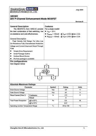
SHANGHAI July 2005 MICROELECTRONICS CO., LTD. SE2301 20V P-Channel Enhancement-Mode MOSFET Revision B General Description Features The MOSFETs from SINO-IC provide For a single mosfet the best combination of fast switching, low VDS = -20 V on-resistance and cost-effectiveness. RDS(ON) = 100m @ VGS=-4.50V @Ids=-2.8A RDS(ON) = 150m @ VGS=-2.50V @Ids=-2.0A Gener
vs2301bc.pdf
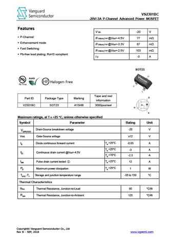
VS2301BC -20V/-3A P-Channel Advanced Power MOSFET Features V DS -20 V P-Channel R DS(on),TYP @VGS=-4.5V 77 m Enhancement mode R DS(on),TYP @VGS=-3.3V 87 m Fast Switching R DS(on),TYP @VGS=-2.5V 103 m Pb-free lead plating; RoHS compliant I D -3 A SOT23 Tape and reel Part ID Package Type Marking information V2301BC SOT23 A1SHB 3000pcs/ree
sm2301.pdf
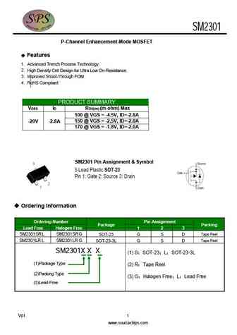
SM2301 P-Channel Enhancement-Mode MOSFET Features 1 Advanced Trench Process Technology. 2 High Density Cell Design for Ultra Low On-Resistance. 3 Improved Shoot-Through FOM 4 RoHS Compliant PRODUCT SUMMARY VDSS ID RDS(on) (m-ohm) Max 100 @ VGS = -4.5V, ID=-2.8A 150 @ VGS = -2.5V, ID=-2.0A -20V -2.8A 170 @ VGS = -1.8V, ID=-2.0A SM2301 Pin Assignment &

ao2301.pdf

AO2301 www.VBsemi.tw P-Channel 20-V (D-S) MOSFET FEATURES MOSFET PRODUCT SUMMARY Halogen-free According to IEC 61249-2-21 VDS (V) RDS(on) ( )ID (A)a Qg (Typ.) Definition 0.035 at VGS = - 10 V - 5e TrenchFET Power MOSFET e - 20 0.043 at VGS = - 4.5 V - 5 10 nC 100 % Rg Tested 0.061 at VGS = - 2.5 V - 4.8 Compliant to RoHS Directive 2002/95/EC APPLICATIONS
af2301pwl.pdf
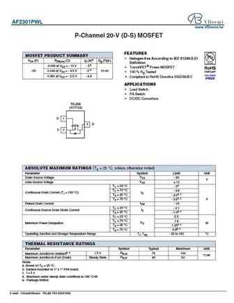
AF2301PWL www.VBsemi.tw P-Channel 20-V (D-S) MOSFET FEATURES MOSFET PRODUCT SUMMARY Halogen-free According to IEC 61249-2-21 VDS (V) RDS(on) ( )ID (A)a Qg (Typ.) Definition 0.035 at VGS = - 10 V - 5e TrenchFET Power MOSFET e - 20 0.043 at VGS = - 4.5 V - 5 10 nC 100 % Rg Tested 0.061 at VGS = - 2.5 V - 4.8 Compliant to RoHS Directive 2002/95/EC APPLICATIONS
ces2301.pdf

CES2301 www.VBsemi.tw P-Channel 20-V (D-S) MOSFET FEATURES MOSFET PRODUCT SUMMARY Halogen-free According to IEC 61249-2-21 VDS (V) RDS(on) ( )ID (A)a Qg (Typ.) Definition 0.035 at VGS = - 10 V - 5e TrenchFET Power MOSFET e - 20 0.043 at VGS = - 4.5 V - 5 10 nC 100 % Rg Tested 0.061 at VGS = - 2.5 V - 4.8 Compliant to RoHS Directive 2002/95/EC APPLICATIONS
mtp2301n3.pdf
MTP2301N3 www.VBsemi.tw P-Channel 20-V (D-S) MOSFET FEATURES MOSFET PRODUCT SUMMARY Halogen-free According to IEC 61249-2-21 VDS (V) RDS(on) ( )ID (A)a Qg (Typ.) Definition 0.035 at VGS = - 10 V - 5e TrenchFET Power MOSFET e - 20 0.043 at VGS = - 4.5 V - 5 10 nC 100 % Rg Tested 0.061 at VGS = - 2.5 V - 4.8 Compliant to RoHS Directive 2002/95/EC APPLICATIONS
ut2301g-ae3-r.pdf
UT2301G-AE3-R www.VBsemi.tw P-Channel 20-V (D-S) MOSFET FEATURES MOSFET PRODUCT SUMMARY Halogen-free According to IEC 61249-2-21 VDS (V) RDS(on) ( )ID (A)a Qg (Typ.) Definition 0.035 at VGS = - 10 V - 5e TrenchFET Power MOSFET e - 20 0.043 at VGS = - 4.5 V - 5 10 nC 100 % Rg Tested 0.061 at VGS = - 2.5 V - 4.8 Compliant to RoHS Directive 2002/95/EC APPLIC
si2301ads-t1.pdf

SI2301ADS-T1 www.VBsemi.tw P-Channel 20-V (D-S) MOSFET FEATURES MOSFET PRODUCT SUMMARY Halogen-free According to IEC 61249-2-21 VDS (V) RDS(on) ( )ID (A)a Qg (Typ.) Definition 0.035 at VGS = - 10 V - 5e TrenchFET Power MOSFET e - 20 0.043 at VGS = - 4.5 V - 5 10 nC 100 % Rg Tested 0.061 at VGS = - 2.5 V - 4.8 Compliant to RoHS Directive 2002/95/EC APPLICATION
si2301cds-t1.pdf

SI2301CDS-T1 www.VBsemi.tw P-Channel 20-V (D-S) MOSFET FEATURES MOSFET PRODUCT SUMMARY Halogen-free According to IEC 61249-2-21 VDS (V) RDS(on) ( )ID (A)a Qg (Typ.) Definition 0.035 at VGS = - 10 V - 5e TrenchFET Power MOSFET e - 20 0.043 at VGS = - 4.5 V - 5 10 nC 100 % Rg Tested 0.061 at VGS = - 2.5 V - 4.8 Compliant to RoHS Directive 2002/95/EC APPLICATION
dmg2301u.pdf

DMG2301U www.VBsemi.tw P-Channel 20-V (D-S) MOSFET FEATURES MOSFET PRODUCT SUMMARY Halogen-free According to IEC 61249-2-21 VDS (V) RDS(on) ( )ID (A)a Qg (Typ.) Definition 0.035 at VGS = - 10 V - 5e TrenchFET Power MOSFET e - 20 0.043 at VGS = - 4.5 V - 5 10 nC 100 % Rg Tested 0.061 at VGS = - 2.5 V - 4.8 Compliant to RoHS Directive 2002/95/EC APPLICATION
apm2301ac.pdf

APM2301AC www.VBsemi.tw P-Channel 20-V (D-S) MOSFET FEATURES MOSFET PRODUCT SUMMARY Halogen-free According to IEC 61249-2-21 VDS (V) RDS(on) ( )ID (A)a Qg (Typ.) Definition 0.035 at VGS = - 10 V - 5e TrenchFET Power MOSFET e - 20 0.043 at VGS = - 4.5 V - 5 10 nC 100 % Rg Tested 0.061 at VGS = - 2.5 V - 4.8 Compliant to RoHS Directive 2002/95/EC APPLICATIO
si2301bds-t1-ge3.pdf
SI2301BDS-T1-GE3 www.VBsemi.tw P-Channel 20-V (D-S) MOSFET FEATURES MOSFET PRODUCT SUMMARY Halogen-free According to IEC 61249-2-21 VDS (V) RDS(on) ( )ID (A)a Qg (Typ.) Definition 0.035 at VGS = - 10 V - 5e TrenchFET Power MOSFET e - 20 0.043 at VGS = - 4.5 V - 5 10 nC 100 % Rg Tested 0.061 at VGS = - 2.5 V - 4.8 Compliant to RoHS Directive 2002/95/EC APPLICA
kd2301.pdf
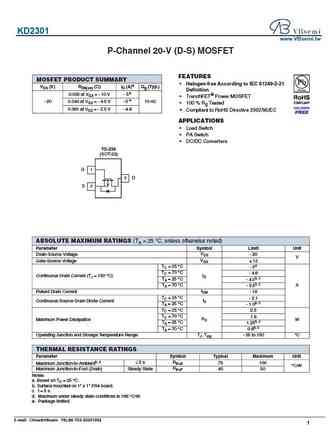
KD2301 www.VBsemi.tw P-Channel 20-V (D-S) MOSFET FEATURES MOSFET PRODUCT SUMMARY Halogen-free According to IEC 61249-2-21 VDS (V) RDS(on) ( )ID (A)a Qg (Typ.) Definition 0.035 at VGS = - 10 V - 5e TrenchFET Power MOSFET e - 20 0.043 at VGS = - 4.5 V - 5 10 nC 100 % Rg Tested 0.061 at VGS = - 2.5 V - 4.8 Compliant to RoHS Directive 2002/95/EC APPLICATIONS

hm2301kr.pdf
HM2301KR www.VBsemi.tw P-Channel 20 V (D-S) MOSFET FEATURES PRODUCT SUMMARY Halogen-free According to IEC 61249-2-21 VDS (V) RDS(on) ( )ID (A)c Qg (Typ.) Definition 0.080 at VGS = - 4.5 V - 3.1 TrenchFET Power MOSFET 4.3 nC - 20 0.100 at VGS = - 2.5 V - 2.3 100 % Rg Tested Compliant to RoHS Directive 2002/95/EC APPLICATIONS Load Switch DC/DC Convert
si2301ds-t1-ge3.pdf

SI2301DS-T1-GE3 www.VBsemi.tw P-Channel 20-V (D-S) MOSFET FEATURES MOSFET PRODUCT SUMMARY Halogen-free According to IEC 61249-2-21 VDS (V) RDS(on) ( )ID (A)a Qg (Typ.) Definition 0.035 at VGS = - 10 V - 5e TrenchFET Power MOSFET e - 20 0.043 at VGS = - 4.5 V - 5 10 nC 100 % Rg Tested 0.061 at VGS = - 2.5 V - 4.8 Compliant to RoHS Directive 2002/95/EC APPLICAT
yjl2301g.pdf
RoHS COMPLIANT YJL2301G P-Channel Enhancement Mode Field Effect Transistor Product Summary V -15V DS I -2.0A D R ( at V =-4.5V) 100 mohm DS(ON) GS R ( at V =-2.5V) 130 mohm DS(ON) GS R ( at V =-1.8V) 230 mohm DS(ON) GS General Description Trench Power LV MOSFET technology Low R DS(ON) Low Gate Charge Applications
yjl2301d.pdf
RoHS COMPLIANT YJL2301D P-Channel Enhancement Mode Field Effect Transistor Product Summary V -15V DS I -3.8A D R ( at V =-4.5V) 52 mohm DS(ON) GS R ( at V =-2.5V) 78 mohm DS(ON) GS R ( at V =-1.8V) 110 mohm DS(ON) GS General Description Trench Power LV MOSFET technology Low R DS(ON) Low Gate Charge Applications Vi
yjl2301f.pdf
RoHS COMPLIANT YJL2301F P-Channel Enhancement Mode Field Effect Transistor Product Summary V -20V DS I -2A D R ( at V =-4.5V) 120 mohm DS(ON) GS R ( at V =-2.5V) 150 mohm DS(ON) GS R ( at V =-1.8V) 250 mohm DS(ON) GS General Description Trench Power LV MOSFET technology Low R DS(ON) Low Gate Charge Applications Vi
yjs2301a.pdf
RoHS COMPLIANT YJS2301A P-Channel Enhancement Mode Field Effect Transistor Product Summary V -20V DS I -3.7A D R ( at V =-4.5V) 64 mohm DS(ON) GS R ( at V =-2.5V) 80 mohm DS(ON) GS R ( at V =-1.8V) 110 mohm DS(ON) GS General Description Trench Power LV MOSFET technology Low R DS(ON) Low Gate Charge Applications Vi
yjl2301c.pdf
RoHS COMPLIANT YJL2301C P-Channel Enhancement Mode Field Effect Transistor Product Summary V -20V DS I -3.4A D R ( at V =-4.5V) 64 mohm DS(ON) GS R ( at V =-2.5V) 80 mohm DS(ON) GS R ( at V =-1.8V) 110 mohm DS(ON) GS General Description Trench Power LV MOSFET technology High Power and Current handing capability Low Gate Ch
ttx2301a.pdf
TTX2301A Wuxi Unigroup Microelectronics CO.,LTD. 20V P-Channel Trench MOSFET(Preliminary) General Description Product Summary Trench Power technology VDS -20V Low RDS(ON) ID (at VGS =-4.5V) -2.6A Low Gate Charge RDS(ON) (at VGS =-10V)
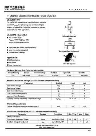
hm2301a.pdf

HM2301A P-Channel Enhancement Mode Power MOSFET DESCRIPTION D The HM2301A uses advanced trench technology to provide excellent RDS(ON), low gate charge and operation with gate G voltages as low as 2.5V. This device is suitable for use as a load switch or in PWM applications. S GENERAL FEATURES Schematic diagram VDS = -20V,ID = -3A RDS(ON)
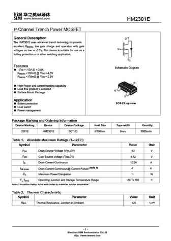
hm2301c.pdf

HM2301 P-Channel Trench Power MOSFET General Description The HM2301 uses advanced trench technology to provide excellent R , low gate charge and operation with gate DS(ON) voltages as low as -2.5V. This device is suitable for use as a battery protection or in other switching application. Features Schematic Diagram VDS = -12V,ID =-2. A R
hm2301.pdf
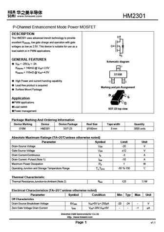
HM2301 P-Channel Enhancement Mode Power MOSFET DESCRIPTION D The HM2301 uses advanced trench technology to provide excellent RDS(ON), low gate charge and operation with gate G voltages as low as 2.5V. This device is suitable for use as a load switch or in PWM applications. S GENERAL FEATURES Schematic diagram VDS = -20V,ID = -3A RDS(ON)
hm2301bkr.pdf
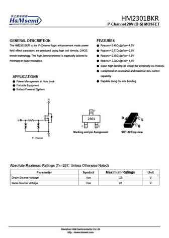
HM2301BKR P-Channel 20V (D-S) MOSFET GENERAL DESCRIPTION FEATURES The HM2301BKR is the P-Channel logic enhancement mode power RDS(ON)= 0.48 @VGS=-4.5V field effect transistors are produced using high cell density, DMOS RDS(ON)= 0.67 @VGS=-2.5V trench technology. This high density process is especially tailored to RDS(ON)= 0.95 @VGS=-1.8V minimize on-state resist
hm2301bsr.pdf

HM2301BSR P-Channel 20V (D-S) MOSFET GENERAL DESCRIPTION FEATURES The HM2301BSR is the P-Channel logic enhancement mode power RDS(ON)= 0.48 @VGS=-4.5V field effect transistors are produced using high cell density, DMOS RDS(ON)= 0.67 @VGS=-2.5V trench technology. This high density process is especially tailored to RDS(ON)= 0.95 @VGS=-1.8V minimize on-state resist
hm2301b.pdf
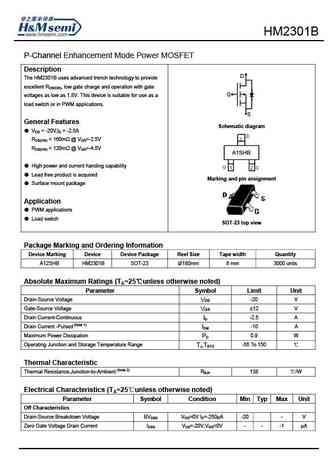
HM2301B P-Channel Enhancement Mode Power MOSFET Description D The HM2301B uses advanced trench technology to provide excellent RDS(ON), low gate charge and operation with gate G voltages as low as 1.8V. This device is suitable for use as a load switch or in PWM applications. S General Features Schematic diagram VDS = -20V,ID = -2.5A RDS(ON)
hm2301e.pdf
HM2301E P-Channel Trench Power MOSFET General Description The HM2301E uses advanced trench technology to provide excellent R , low gate charge and operation with gate DS(ON) voltages as low as -2.5V. This device is suitable for use as a battery protection or in other switching application. Features Schematic Diagram VDS = -12V,ID =-2.0A R
hm2301bjr.pdf
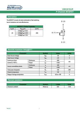
HM2301BJR P-Channel MOSFET Description The MOSFET provide the best combination of fast switching, D 3 low on-resistance and cost-effectiveness. MOSFET Product Summary V (V) R ( ) I (mA) DS DS(on) D 0.45@ V =-4.5V GS G 1 -20 0.62@ VGS=-2.5V -800 0.86@ V =-1.8V GS S 2 Absolute maximum rating@25 Parameter Symbol Value Units Drain-Source Voltage
hm2301dr.pdf
H P-Channel 20V (D-S) MOSFET GENERAL DESCRIPTION FEATURES The is the P-Channel logic enhancement mode power RDS(ON)= 0.48 @VGS=-4.5V field effect transistors are produced using high cell density, DMOS RDS(ON)= 0.67 @VGS=-2.5V trench technology. This high density process is especially tailored to RDS(ON)= 0.95 @VGS=-1.8V minimize on-state resistan
hm2301d.pdf
H P-Channel 20V (D-S) MOSFET GENERAL DESCRIPTION FEATURES The is the P-Channel logic enhancement mode power RDS(ON)= 0.48 @VGS=-4.5V field effect transistors are produced using high cell density, DMOS RDS(ON)= 0.67 @VGS=-2.5V trench technology. This high density process is especially tailored to RDS(ON)= 0.95 @VGS=-1.8V minimize on-state resistance
hm2301kr.pdf
HM2301KR P-Channel Enhancement Mode Power MOSFET DESCRIPTION D The HM2301KR uses advanced trench technology to provide excellent RDS(ON), low gate charge and operation with gate G voltages as low as 2.5V. This device is suitable for use as a load switch or in PWM applications. S GENERAL FEATURES Schematic diagram VDS = -20V,ID = -3A RDS(ON)
hm2301f.pdf
HM2301F P-Channel Enhancement Mode Power MOSFET Description D The HM2301F uses advanced trench technology to provide excellent RDS(ON), low gate charge and operation with gate G voltages as low as 1.8V. This device is suitable for use as a load switch or in PWM applications. S General Features Schematic diagram VDS = -20V,ID = -2.8A RDS(ON)
hpm2301.pdf
HPM2301 P-Channel MOSFETs -2.8A,-20V P P HPM2301 P-Channel Enhancement-Mode MOS FETs P-Channel Enhancement Features Mode MOS FETs -20V, -2.8A, RDS(ON)=100m @ VGS=-10V High dense cell design for extremely low RDS(ON) Rugged and reliable Lea
h2301.pdf
HAOHAI ELECTRONICS H2301 - 2A, -20V, P-Channel MOSFET APPLICATIONS Load switch for portable Features DC/DC converter RDS(ON) 120m @ VGS=-4.5V FEATURE RDS(ON) 170m @ VGS=-2.5V High Density Cell Design For Ultra Industry-standard pinout SOT-23 Package Low On-Resistance Compatible with Existing Surface MountTechniques
pm2301.pdf
PM2301 20V P-Channel MOSFET Description Applications The PM2301 uses advanced Trench technology and designs to provide excellent R with low gate charge. PA Switch DS(ON) This device is suitable for use in PWM, load switching and Load Switch general purpose applications. Marking Information Features TrenchFET Power MOSFET 2301 Dimensions and Pin Configurati
ap2301bi.pdf
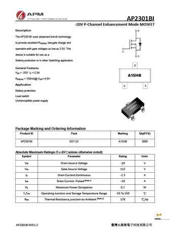
AP2301BI -20V P-Channel Enhancement Mode MOSFET Description The AP2301BI uses advanced trench technology to provide excellent R , low gate charge and DS(ON) operation with gate voltages as low as 2.5V. This device is suitable for use as a Battery protection or in other Switching application. General Features V = -20V I =-2.3A DS D R
ap2301ai.pdf
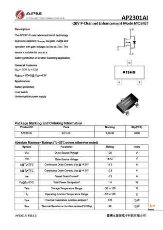
AP2301AI -20V P-Channel Enhancement Mode MOSFET Description The AP2301AI uses advanced trench technology to provide excellent R , low gate charge and DS(ON) operation with gate voltages as low as 2.5V. This device is suitable for use as a Battery protection or in other Switching application. General Features V = -20V I =-3.3A DS D R
Другие IGBT... SSS5N60, SSS7N60, SSS8N60, 1002, 1115, 1515, G1601, 2300, IRFB3206, 2302, 3035, 3400, 3401, 3415, 6616, 6703, 6760
Параметры MOSFET. Взаимосвязь и компромиссы
History: AON7506 | DH028N03F | SSS2N80A | DH028N03I
🌐 : EN ES РУ

Список транзисторов
Обновления
MOSFET: CS95118 | CS85105A | CS75N45 | CS72N12 | CS55N50 | CS48N75A | CS40N27 | MSQ60P04D | MSQ40P07D | MSQ30P40D | MSQ30P15 | MSQ30P07D | MSQ100N03D | MSHM60P14 | MSHM40N085 | MSHM30N46
Popular searches
bc182b | 2n3054 transistor equivalent | 2n554 | 2sa1011 | 2sa1283 | 2sb646 | 2sc1885 datasheet | 2sc2580