3400 datasheet, аналоги, основные параметры
Наименование производителя: 3400 📄📄
Тип транзистора: MOSFET
Полярность: N
Предельные значения
Pd ⓘ - Максимальная рассеиваемая мощность: 1.4 W
|Vds|ⓘ - Максимально допустимое напряжение сток-исток: 30 V
|Vgs|ⓘ - Максимально допустимое напряжение затвор-исток: 12 V
|Id| ⓘ - Максимально допустимый постоянный ток стока: 5.8 A
Tj ⓘ - Максимальная температура канала: 150 °C
Электрические характеристики
tr ⓘ - Время нарастания: 4.8 ns
Cossⓘ - Выходная емкость: 99 pf
RDSonⓘ - Сопротивление сток-исток открытого транзистора: 0.035 Ohm
Тип корпуса: SOT23
📄📄 Копировать
Аналог (замена) для 3400
- подборⓘ MOSFET транзистора по параметрам
3400 даташит
3400.pdf
GOFORD 3400 DESCRIPTION The 3400 uses advanced trench technology to provide D excellent RDS(ON), low gate charge and operation with gate voltages as low as 2.5V. This device is suitable for use as a G Battery protection or in other Switching application. GENERAL FEATURES S Schematic diagram VDSS RDS(ON) RDS(ON) RDS(ON) ID @ 4.5V (Typ) @ 2.5V (Typ) @ 10V (Typ) m m
3400.pdf
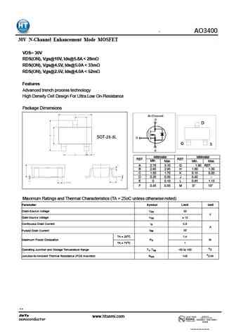
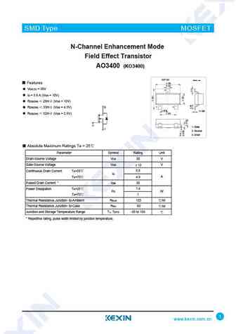
3400 N-Channel Enhancement Mode Field Effect Transistor V(BR)DSS RDS(ON)MAX ID SOT-23 35m @10V SOT-23 Plastic-Encapsulate MOSFET 30V 40m @4.5V 5.8A 52m @2.5V Features SOT-23 High dense cell design for extremely low RDS(on). Exceptional on-resistance and maximum DC current capability. Load/Power Switching. Interfacing Swi
fcd3400n80z fcu3400n80z.pdf
March 2015 FCD3400N80Z / FCU3400N80Z N-Channel SuperFET II MOSFET 800 V, 2 A, 3.4 Features Description RDS(on) = 2.75 (Typ.) SuperFET II MOSFET is Fairchild Semiconductor s brand-new high voltage super-junction (SJ) MOSFET family that is utilizing Ultra Low Gate Charge (Typ. Qg = 7.4 nC) charge balance technology for outstanding low on-resistance Low Eoss (Typ.
dmc3400sdw.pdf
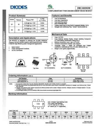
DMC3400SDW COMPLEMENTARY PAIR ENHANCEMENT MODE MOSFET Product Summary Features and Benefits Low On-Resistance ID max Device V(BR)DSS RDS(ON) max Low Input Capacitance TA = +25 C Fast Switching Speed 0.4 @ VGS = 10V 0.65A ESD Protected Gate Q1 30 Totally Lead-Free & Fully RoHS Compliant (Notes 1 & 2) 0.7 @ VGS = 4.5V 0.52A Halogen an
sil3400a.pdf
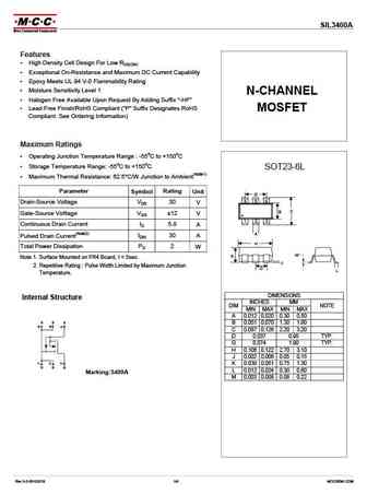
SIL3400A Features High Density Cell Design For Low RDS(ON) Exceptional On-Resistance and Maximum DC Current Capability Epoxy Meets UL 94 V-0 Flammability Rating Moisture Sensitivity Level 1 N-CHANNEL Halogen Free Available Upon Request By Adding Suffix "-HF" Lead Free Finish/RoHS Compliant ("P" Suffix Designates RoHS MOSFET Compliant. See Ordering Information)
si3400a.pdf
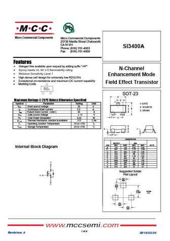
M C C R Micro Commercial Components Micro Commercial Components 20736 Marilla Street Chatsworth CA 91311 SI3400A Phone (818) 701-4933 Fax (818) 701-4939 Features Halogen free available upon request by adding suffix "-HF" N-Channel Epoxy meets UL 94 V-0 flammability rating Moisture Sensitivity Level 1 Enhancement Mode High dense cell design for extremely low
fcd3400n80z fcu3400n80z.pdf

Is Now Part of To learn more about ON Semiconductor, please visit our website at www.onsemi.com Please note As part of the Fairchild Semiconductor integration, some of the Fairchild orderable part numbers will need to change in order to meet ON Semiconductor s system requirements. Since the ON Semiconductor product management systems do not have the ability to manage part nomenclatur
ut3400l-ae2-r ut3400g-ae2-r ut3400l-ae3-r ut3400g-ae3-r.pdf
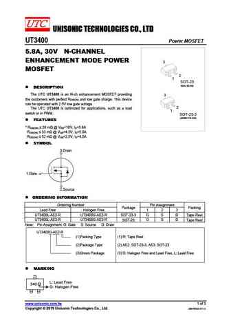
UNISONIC TECHNOLOGIES CO., LTD UT3400 Power MOSFET 5.8A, 30V N-CHANNEL ENHANCEMENT MODE POWER 3 MOSFET 2 1 SOT-23 (EIAJ SC-59) DESCRIPTION The UTC UT3400 is an N-ch enhancement MOSFET providing 3 the customers with perfect RDS(ON) and low gate charge. This device can be operated with 2.5V low gate voltage. 2 The UTC UT3400 is optimized for applications, such as a lo
ut3400.pdf
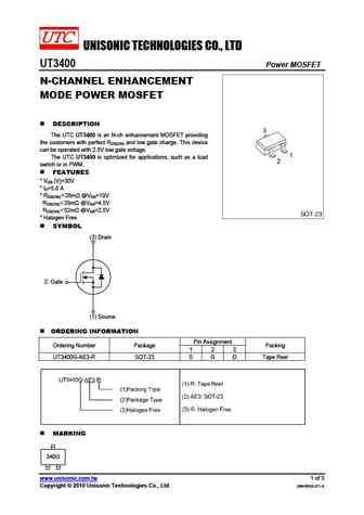
UNISONIC TECHNOLOGIES CO., LTD UT3400 Power MOSFET N-CHANNEL ENHANCEMENT MODE POWER MOSFET DESCRIPTION The UTC UT3400 is an N-ch enhancement MOSFET providing the customers with perfect RDS(ON) and low gate charge. This device can be operated with 2.5V low gate voltage. The UTC UT3400 is optimized for applications, such as a load switch or in PWM. FEATURES * VDS (V)=30V
smg3400.pdf
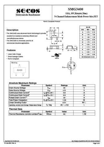
SMG3400 5.8A, 30V,RDS(ON) 28m Elektronische Bauelemente N-Channel Enhancement Mode Power Mos.FET RoHS Compliant Product SC-59 A Dim Min Max Description L A 2.70 3.10 The SMG3400 uses advanced trench technology to provide * 3 B 1.40 1.60 S B Top View excellent on-resistance extremely efficient and 2 1 C 1.00 1.30 cost-effectiveness device. D 0.35 0.50 The SMG3400 is uni
tsm3400cx.pdf
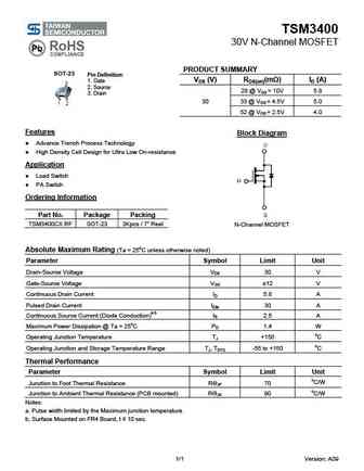
TSM3400 30V N-Channel MOSFET PRODUCT SUMMARY SOT-23 Pin Definition VDS (V) RDS(on)(m ) ID (A) 1. Gate 2. Source 28 @ VGS = 10V 5.8 3. Drain 30 33 @ VGS = 4.5V 5.0 52 @ VGS = 2.5V 4.0 Features Block Diagram Advance Trench Process Technology High Density Cell Design for Ultra Low On-resistance Application Load Switch PA Switch Ordering Infor
cj3400a.pdf
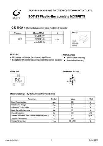
JIANGSU CHANGJIANG ELECTRONICS TECHNOLOGY CO., LTD SOT-23 Plastic-Encapsulate MOSFETS CJ3400A N-Channel Enhancement Mode Field Effect Transistor SOT-23 ID V(BR)DSS RDS(on)MAX 32m @10V 30V 38m @4.5V 5.8A 1. GATE 45m @2.5V 2. SOURCE 3. DRAIN FEATURE APPLICATION High dense cell design for extremely low RDS(ON) Load/Power Switching Exceptional on-resistanc
cj3400-hf.pdf
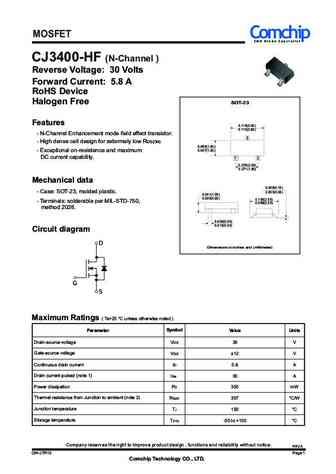
MOSFET Comchip S M D D i o d e S p e c i a l i s t CJ3400-HF (N-Channel ) Reverse Voltage 30 Volts Forward Current 5.8 A RoHS Device Halogen Free SOT-23 Features 0.118(3.00) 0.110(2.80) - N-Channel Enhancement mode field effect transistor. 3 - High dense cell design for extermely low RDS(ON) 0.055(1.40) 0.047(1.20) - Exceptional on-resistance and maximum DC current capab
cj3400.pdf
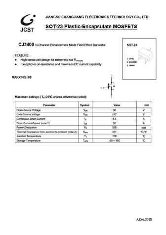
JIANGSU CHANGJIANG ELECTRONICS TECHNOLOGY CO., LTD SOT-23 Plastic-Encapsulate MOSFETS CJ3400 N-Channel Enhancement Mode Field Effect Transistor SOT-23 FEATURE 1. GATE High dense cell design for extremely low RDS(ON) 2. SOURCE Exceptional on-resistance and maximum DC current capability 3. DRAIN MARKING R0 Maximum ratings ( Ta=25 unless otherwise noted) Parameter
cjk3400a.pdf
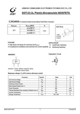
JIANGSU CHANGJIANG ELECTRONICS TECHNOLOGY CO., LTD SOT-23-3L Plastic-Encapsulate MOSFETS CJK3400A N-Channel Enhancement Mode Field Effect Transistor ID V(BR)DSS RDS(on)MAX SOT-23-3L 32m @10V 30V 38m @4.5V 5.8A 45m @2.5V 1. GATE 2. SOURCE 3. DRAIN D FEATURE APPLICATION High dense cell design for extremely low RDS(ON) Load/Power Switching Exceptional on-r
cjk3400ah.pdf
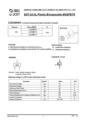
JIANGSU CHANGJING ELECTRONICS TECHNOLOGY CO., LTD SOT-23-3L Plastic-Encapsulate MOSFETS CJK3400AH N-Channel Enhancement Mode Field Effect Transistor ID V(BR)DSS RDS(on)MAX SOT-23-3L 27m @10V 30V 32m @4.5V 5.8A 48m @2.5V 1. GATE 2. SOURCE 3. DRAIN D FEATURE APPLICATION High dense cell design for extremely low RDS(ON) Load/Power Switching Exceptional on-resist
ktc3400.pdf
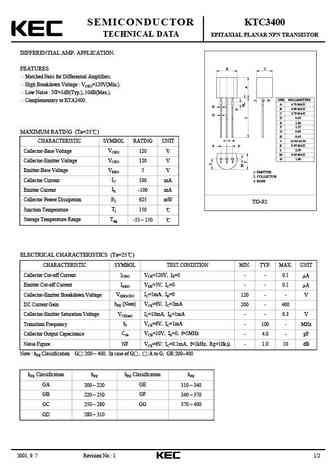
SEMICONDUCTOR KTC3400 TECHNICAL DATA EPITAXIAL PLANAR NPN TRANSISTOR DIFFERENTIAL AMP. APPLICATION. B C FEATURES Matched Pairs for Differential Amplifiers. High Breakdown Voltage VCEO=120V(Min.). Low Noise NF=1dB(Typ.), 10dB(Max.). N DIM MILLIMETERS Complementary to KTA2400. A 4.70 MAX E K B 4.80 MAX G C 3.70 MAX D D 0.45 E 1.00 F 1.27 G 0.85 MAXIMUM RATING (Ta=25 )
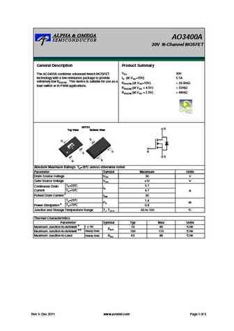
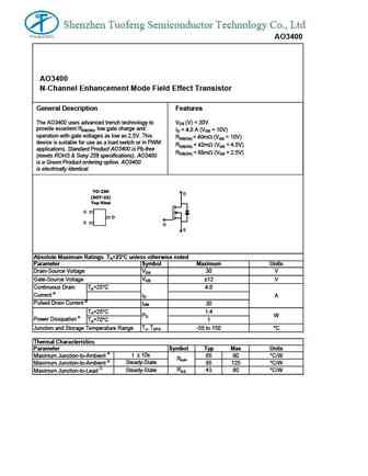
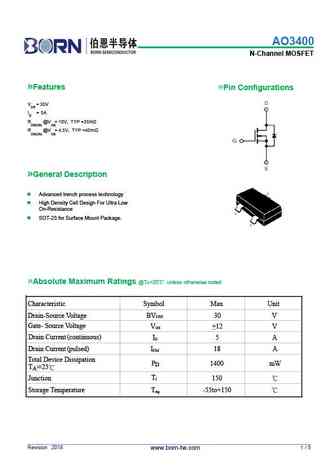
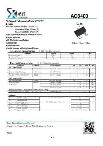
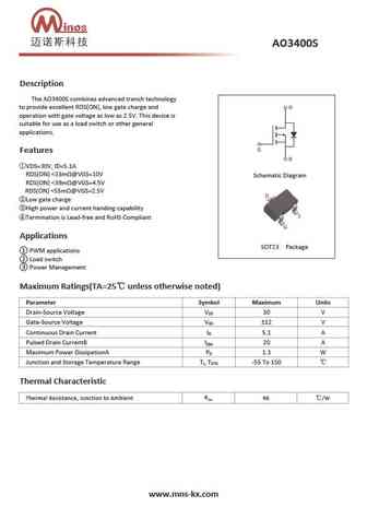
ao3400.pdf
AO3400 30V N-Channel Enhancement Mode MOSFET VDS= 30V RDS(ON), Vgs@10V, Ids@5.8A
ao3400.pdf
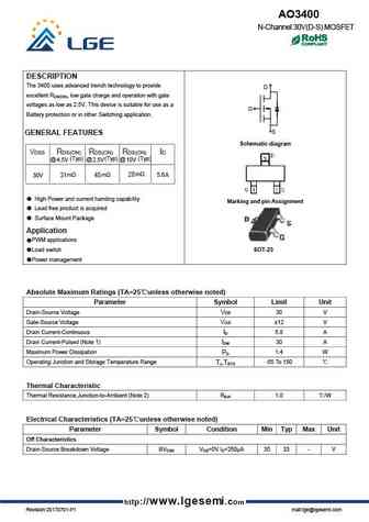
AO3400 N-Channel 30V(D-S) MOSFET DESCRIPTION The 3400 uses advanced trench technology to provide D excellent RDS(ON), low gate charge and operation with gate voltages as low as 2.5V. This device is suitable for use as a G Battery protection or in other Switching application. S GENERAL FEATURES Schematic diagram VDSS RDS(ON) RDS(ON) RDS(ON) ID @ 4.5V (Typ) @ 2.5V (Typ) @ 1
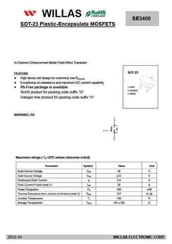
se3400.pdf
FM120-M WILLAS THRU SE3400 FM1200-M 1.0A SURFACE MOUNT SCHOTTKY SOT-23 Plastic-Encapsulate MOSFETS BARRIER RECTIFIERS -20V- 200V SOD-123 PACKAGE Pb Free Produ Package outline Features Batch process design, excellent power dissipation offers better reverse leakage current and thermal resistance. SOD-123H Low profile surface mounted application in order to optimize bo
ao3400c.pdf
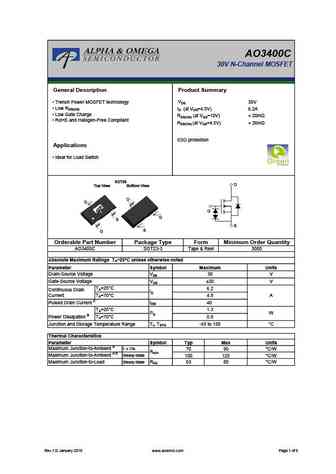
AO3400C 30V N-Channel MOSFET General Description Product Summary VDS Trench Power MOSFET technology 30V Low RDS(ON) ID (at VGS=4.5V) 6.2A Low Gate Charge RDS(ON) (at VGS=10V)
ao3400.pdf
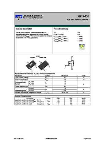
AO3400 30V N-Channel MOSFET General Description Product Summary VDS 30V The AO3400 combines advanced trench MOSFET technology with a low resistance package to provide ID (at VGS=10V) 5.8A extremely low RDS(ON). This device is suitable for use as a RDS(ON) (at VGS=10V)
am3400n.pdf
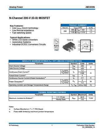
Analog Power AM3400N N-Channel 200-V (D-S) MOSFET PRODUCT SUMMARY Key Features rDS(on) (m ) VDS (V) ID (A) Low r trench technology DS(on) 950 @ VGS = 10V 1.2 Low thermal impedance 200 1100 @ VGS = 5.5V 1.1 Fast switching speed Typical Applications White LED boost converters TSOP-6 Automotive Systems Industrial DC/DC Conversion Circuits ABSOL
afn3400.pdf
AFN3400 Alfa-MOS 30V N-Channel Technology Enhancement Mode MOSFET General Description Features AFN3400, N-Channel enhancement mode 30V/4.0A,RDS(ON)=48m @VGS=10V MOSFET, uses Advanced Trench Technology 30V/3.5A,RDS(ON)=52m @VGS=4.5V to provide excellent RDS(ON), low gate charge. 30V/2.8A,RDS(ON)=58m @VGS=2.5V These devices are particularly suited for low Super
afn3400s.pdf
AFN3400S Alfa-MOS 30V N-Channel Technology Enhancement Mode MOSFET General Description Features AFN3400S, N-Channel enhancement mode 30V/4.0A,RDS(ON)=42m @VGS=10V MOSFET, uses Advanced Trench Technology 30V/3.0A,RDS(ON)=44m @VGS=4.5V to provide excellent RDS(ON), low gate charge. 30V/2.6A,RDS(ON)=50m @VGS=2.5V These devices are particularly suited for low Sup
afn3400as.pdf
AFN3400AS Alfa-MOS 30V N-Channel Technology Enhancement Mode MOSFET General Description Features AFN3400AS, N-Channel enhancement mode 30V/2.8A,RDS(ON)=46m @VGS=10V MOSFET, uses Advanced Trench Technology 30V/2.5A,RDS(ON)=50m @VGS=4.5V to provide excellent RDS(ON), low gate charge. 30V/2.2A,RDS(ON)=58m @VGS=2.5V These devices are particularly suited for low 3
afn3400a.pdf
AFN3400A Alfa-MOS 30V N-Channel Technology Enhancement Mode MOSFET General Description Features AFN3400A, N-Channel enhancement mode 30V/2.4A,RDS(ON)=54m @VGS=10V MOSFET, uses Advanced Trench Technology 30V/1.8A,RDS(ON)=58m @VGS=4.5V to provide excellent RDS(ON), low gate charge. 30V/1.5A,RDS(ON)=65m @VGS=2.5V These devices are particularly suited for low 30V
ao3400.pdf
Shenzhen Tuofeng Semiconductor Technology Co., Ltd AO3400 AO3400 N-Channel Enhancement Mode Field Effect Transistor General Description Features The AO3400 uses advanced trench technology to VDS (V) = 30V provide excellent RDS(ON), low gate charge and ID = 4.8 A (VGS = 10V) operation with gate voltages as low as 2.5V. This RDS(ON)
mtn3400n3.pdf
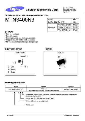
Spec. No. C414N3 Issued Date 2007.07.05 CYStech Electronics Corp. Revised Date 2017.05.03 Page No. 1/ 9 30V N-CHANNEL Enhancement Mode MOSFET BVDSS 30V MTN3400N3 ID@VGS=10V, TA=25 C 5.8A 20m VGS=10V, ID=5.8A 22m RDSON(TYP) VGS=4.5V, ID=5A 27m VGS=2.5V, ID=4A Features Low on-resistance Low gate charge Excellent thermal and electrical
3400h.pdf
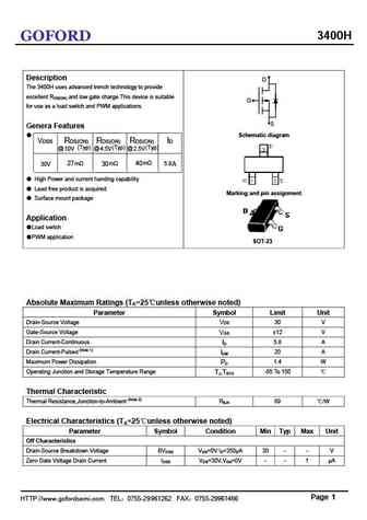
3400H GOFORD Description D The 3400H uses advanced trench technology to provide excellent RDS(ON) and low gate charge.This device is suitable G for use as a load switch and PWM applications. S Genera Features Schematic diagram VDSS RDS(ON) RDS(ON) RDS(ON) ID @ (Typ) @ 10V 4.5V (Typ) @ 2.5V (Typ) m 27 m m 40 5.8 30V 30 A High Power and current handing cap
3400l.pdf
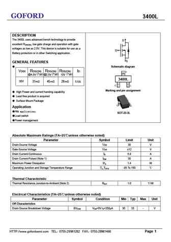
GOFORD 3400L DESCRIPTION The 3400L uses advanced trench technology to provide D excellent RDS(ON), low gate charge and operation with gate voltages as low as 2.5V. This device is suitable for use as a G Battery protection or in other Switching application. S GENERAL FEATURES Schematic diagram VDSS RDS(ON) RDS(ON) RDS(ON) ID @4.5V (Typ) @2.5V (Typ) (Typ) 10V 3400L 3
sts3400.pdf
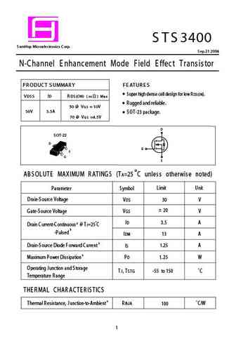
S TS 3400 S amHop Microelectronics C orp. S ep.21 2004 N-Channel E nhancement Mode Field E ffect Transistor PR ODUC T S UMMAR Y F E ATUR E S S uper high dense cell design for low R DS (ON). VDS S ID R DS (ON) ( m ) Max R ugged and reliable. 50 @ VG S = 10V 30V 3.5A S OT-23 package. 70 @ VG S =4.5V D S OT-23 G S AB S OLUTE MAXIMUM R ATINGS (TA=25 C unless otherwise noted) Li
ao3400.pdf
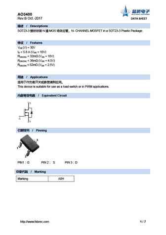
AO3400 Rev.B Oct.-2017 DATA SHEET / Descriptions SOT23-3 N MOS N- CHANNEL MOSFET in a SOT23-3 Plastic Package. / Features VDS (V) = 30V ID = 5.8 A (VGS = 10V) RDS(ON)
ftk3400.pdf
SEMICONDUCTOR FTK3400 TECHNICAL DATA N-Channel Enhancement Mode Field Effect Transistor D FEATURE G High dense cell design for extremely low R S DS(ON) Schematic diagram Exceptional on-resistance and maximum DC current capability D 3 R0 G 1 2 S Marking and pin Assignment SOT-23 top view Maximum ratings ( Ta=25 unless otherwise noted) Parameter Symbol Value Unit
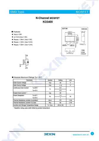
ko3400 ao3400.pdf
SMD Type IC SMD Type MOSFET N-Channel Enhancement Mode Field Effect Transistor KO3400(AO3400) SOT-23 Unit mm +0.1 Features 2.9-0.1 +0.1 0.4-0.1 VDS (V) = 30V 3 ID =5.8 A(VGS =10V) RDS(ON) 28m (VGS = 10V) 12 RDS(ON) 33m (VGS =4.5V) +0.1 +0.05 0.95-0.1 0.1-0.01 +0.1 1.9-0.1 RDS(ON) 52m (VGS =2.5V) 1.Base 1. Gate 2.Emitter 2. Source 3. Drain 3.collector Absolute Maxim
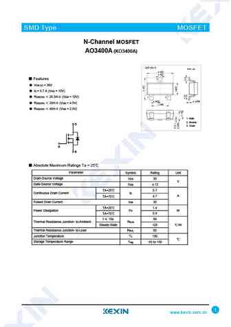
ao3400a.pdf
SMD Type MOSFET N-Channel MOSFET AO3400A (KO3400A) SOT-23 Unit mm +0.1 2.9 -0.1 0.4+0.1 -0.1 3 Features VDS (V) = 30V ID = 5.7 A (VGS = 10V) 1 2 RDS(ON) 26.5m (VGS = 10V) +0.1 +0.05 0.95 -0.1 0.1 -0.01 +0.1 1.9 -0.1 RDS(ON) 32m (VGS = 4.5V) RDS(ON) 48m (VGS = 2.5V) 1. Gate 2. Source 3. Drain D D G G S S Absolute
ao3400-3.pdf
SMD Type IC SMD Type MOSFET N-Channel Enhancement MOSFET AO3400 (KO3400) SOT-23-3 Unit mm +0.2 2.9 -0.1 Features +0.1 0.4-0.1 3 VDS (V) = 30V ID = 5.8 A (VGS = 10V) RDS(ON) 28m (VGS = 10V) 1 2 RDS(ON) 33m (VGS = 4.5V) +0.02 +0.1 0.15 -0.02 0.95 -0.1 RDS(ON) 52m (VGS = 2.5V) D +0.1 1.9 -0.2 1. Gate 2. Source G S 3. Drain Absolute Maximum Ratings Ta = 25 Parameter Sy
ko3400-89.pdf
SMD Type IC SMD Type MOSFET N-Channel MOSFET KO3400 SOT-89 Unit mm Features 1.70 0.1 VDS (V) = 30V ID = 5.8 A (VGS = 10V) RDS(ON) 28m (VGS = 10V) RDS(ON) 33m (VGS = 4.5V) RDS(ON) 52m (VGS = 2.5V) 0.42 0.1 0.46 0.1 1.Gate 2.Drain 3.Source D G S Absolute Maximum Ratings Ta = 25 Parameter Symbol Rating Unit Drain-Source Voltage VDS 30 V Gate-Source Voltage VGS 12 V Continu
ao3400a-3.pdf
SMD Type MOSFET N-Channel MOSFET AO3400A (KO3400A) SOT-23-3 Unit mm +0.2 2.9 -0.1 +0.1 0.4-0.1 3 Features VDS (V) = 30V ID = 5.7 A (VGS = 10V) RDS(ON) 26.5m (VGS = 10V) 1 2 +0.02 +0.1 0.15 -0.02 0.95 -0.1 RDS(ON) 32m (VGS = 4.5V) +0.1 1.9 -0.2 RDS(ON) 48m (VGS = 2.5V) 1. Gate 2. Source D D 3. Drain G G S S Absol
ao3400.pdf
SMD Type IC SMD Type MOSFET N-Channel Enhancement Mode Field Effect Transistor AO3400 (KO3400) SOT-23 Unit mm +0.1 Features 2.9 -0.1 +0.1 0.4 -0.1 VDS (V) = 30V 3 ID = 5.8 A (VGS = 10V) RDS(ON) 28m (VGS = 10V) 1 2 RDS(ON) 33m (VGS = 4.5V) +0.1 +0.05 0.95 -0.1 0.1 -0.01 +0.1 1.9 -0.1 RDS(ON) 52m (VGS = 2.5V) 1.Base 1. Gate 2.Emitter 2. Source 3. Drain 3.collector Ab
pja3400.pdf
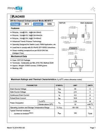
PPJA3400 30V N-Channel Enhancement Mode MOSFET SOT-23 Unit inch(mm) 30 V 4.9A Voltage Current Features RDS(ON) , VGS@10V, ID@4.9A
am3400.pdf
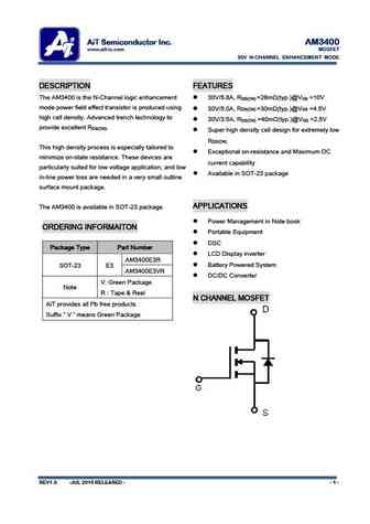
AiT Semiconductor Inc. AM3400 www.ait-ic.com MOSFET 30V N-CHANNEL ENHANCEMENT MODE DESCRIPTION FEATURES The AM3400 is the N-Channel logic enhancement 30V/5.8A, R =28m (typ.)@V =10V DS(ON) GS mode power field effect transistor is produced using 30V/5.0A, R =30m (typ.)@V =4.5V DS(ON) GS high cell density. Advanced trench technology to 30V/3.5A, R =40m (typ.)@V =2.
am3400a.pdf
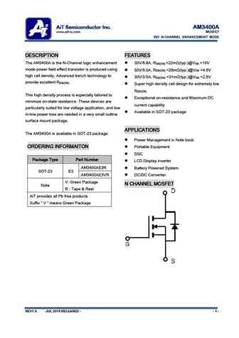
AiT Semiconductor Inc. AM3400A www.ait-ic.com MOSFET 30V N-CHANNEL ENHANCEMENT MODE DESCRIPTION FEATURES The AM3400A is the N-Channel logic enhancement 30V/5.8A, R =22m (typ.)@V =10V DS(ON) GS mode power field effect transistor is produced using 30V/5.0A, R =25m (typ.)@V =4.5V DS(ON) GS high cell density. Advanced trench technology to 30V/3.5A, R =31m (typ.)@V =
blm3400.pdf
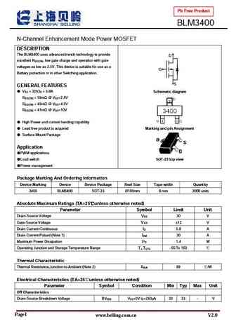
Pb Free Product BLM3400 N-Channel Enhancement Mode Power MOSFET DESCRIPTION The BLM3400 uses advanced trench technology to provide D excellent R , low gate charge and operation with gate DS(ON) voltages as low as 2.5V. This device is suitable for use as a G Battery protection or in other Switching application. S GENERAL FEATURES V = 30V,I = 5.8A Schematic diagram DS
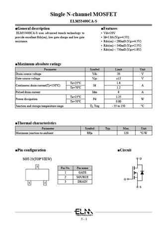
elm13400ca-s.pdf
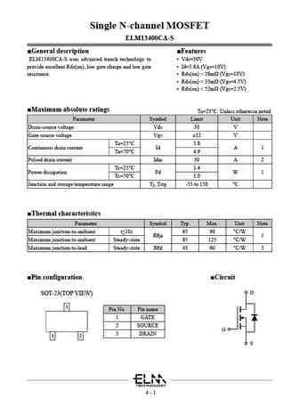
Single N-channel MOSFET ELM13400CA-S General description Features ELM13400CA-S uses advanced trench technology to Vds=30V provide excellent Rds(on), low gate charge and low gate Id=5.8A (Vgs=10V) resistance. Rds(on)
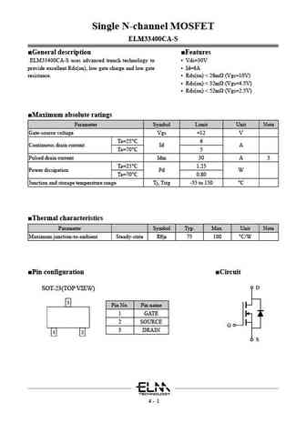
elm53400ca.pdf
Single N-channel MOSFET ELM53400CA-S General description Features ELM53400CA-S uses advanced trench technology to Vds=20V provide excellent Rds(on), low gate charge and low gate Id=1.8A (Vgs=4.5V) resistance. Rds(on)
elm33400ca.pdf
Single N-channel MOSFET ELM33400CA-S General description Features ELM33400CA-S uses advanced trench technology to Vds=30V provide excellent Rds(on), low gate charge and low gate Id=6A resistance. Rds(on)
gsm3400.pdf
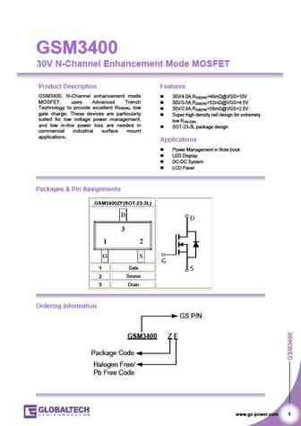
GSM3400 GSM3400 30V N-Channel Enhancement Mode MOSFET Product Description Features GSM3400, N-Channel enhancement mode 30V/4.0A,RDS(ON)=48m @VGS=10V MOSFET, uses Advanced Trench 30V/3.5A,RDS(ON)=52m @VGS=4.5V Technology to provide excellent RDS(ON), low 30V/2.8A,RDS(ON)=58m @VGS=2.5V gate charge. These devices are particularly Super high density cell des
gsm3400a.pdf
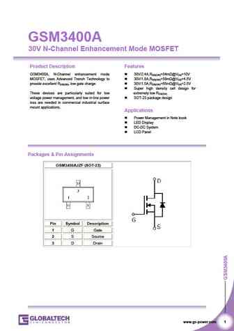
GSM3400A 30V N-Channel Enhancement Mode MOSFET Product Description Features GSM3400A, N-Channel enhancement mode 30V/2.4A,RDS(ON)=54m @VGS=10V MOSFET, uses Advanced Trench Technology to 30V/1.8A,RDS(ON)=58m @VGS=4.5V provide excellent RDS(ON), low gate charge. 30V/1.5A,RDS(ON)=65m @VGS=2.5V Super high density cell design for These devices are particularly suited for lo
gsm3400as.pdf
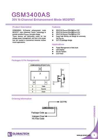
30V N-Channel Enhancement Mode MOSFET Product Description Features GSM3400AS, N-Channel enhancement mode 30V/2.8A,RDS(ON)=50m @VGS=10V MOSFET, uses Advanced Trench Technology to 30V/2.5A,RDS(ON)=55m @VGS=4.5V provide excellent RDS(ON), low gate charge. 30V/2.2A,RDS(ON)=75m @VGS=2.5V These devices are particularly suited for low Super high density cell design for
gsm3400s.pdf
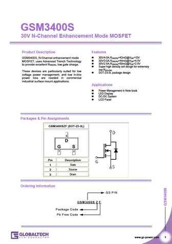
GSM3400S GSM3400S 30V N-Channel Enhancement Mode MOSFET Product Description Features 30V/4.0A,RDS(ON)=42m @VGS=10V GSM3400S, N-Channel enhancement mode 30V/3.0A,RDS(ON)=44m @VGS=4.5V MOSFET, uses Advanced Trench Technology 30V/2.6A,RDS(ON)=50m @VGS=2.5V to provide excellent RDS(ON), low gate charge. Super high density cell design for extremely low RDS (ON) The
kia3400.pdf
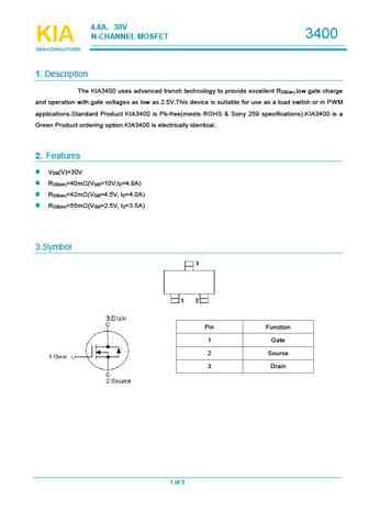
4.8A 30V 3400 N-CHANNELMOSFET KIA KIA KIA SEMICONDUCTORS SEMICONDUCTORS SEMICONDUCTORS 1.Description The KIA3400 uses advanced trench technology to provide excellent R ,lowgate charge DS(on) and operation with gate voltages as lowas 2.5V.This device is suitable for use as a load switch or in PWM applications.Standard Product KIA3400 is Pb-free(meets ROHS & Sony 259 specifications
mmn3400.pdf
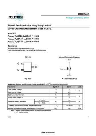
MMN3400 Package Level Data Sheet M-MOS Semiconductor Hong Kong Limited 30V N-Channel Enhancement-Mode MOSFET VDS= 30V RDS(ON), Vgs@10V, Ids@5.8A = 41m RDS(ON), Vgs@4.5V, Ids@5.0A = 45m RDS(ON), Vgs@2.5V, Ids@4.0A = 59m Features Advanced trench process technology High Density Cell Design For Ultra Low On-Resistance SOT-23 Internal Schematic Diagram Drain Gate Source To
nce3400.pdf

Pb Free Product http //www.ncepower.com NCE3400 NCE N-Channel Enhancement Mode Power MOSFET Description D The NCE3400 uses advanced trench technology to provide excellent RDS(ON), low gate charge and operation with gate G voltages as low as 2.5V. This device is suitable for use as a Battery protection or in other Switching application. S General Features Schematic diagram
nce3400xy.pdf
NCE3400XY http //www.ncepower.com NCE N-Channel Enhancement Mode Power MOSFET Description D The NCE3400XY uses advanced trench technology to provide excellent RDS(ON), low gate charge and operation with gate G voltages as low as 2.5V. This device is suitable for use as a Battery protection or in other Switching application. S Schematic diagram General Features VDS = 30
nce3400x.pdf

http //www.ncepower.com NCE3400X NCE N-Channel Enhancement Mode Power MOSFET Description D The NCE3400X uses advanced trench technology to provide excellent RDS(ON), low gate charge and operation with gate G voltages as low as 2.5V. This device is suitable for use as a Battery protection or in other Switching application. S General Features Schematic diagram VDS = 30V,
nce3400ay.pdf

http //www.ncepower.com NCE3400AY NCE N-Channel Enhancement Mode Power MOSFET Description D The NCE3400AY uses advanced trench technology to provide excellent RDS(ON), low gate charge and operation with gate G voltages as low as 2.5V. This device is suitable for use as a Battery protection or in other Switching application. S General Features Schematic diagram VDS = 30
nce3400e.pdf
http //www.ncepower.com NCE3400E NCE N-Channel Enhancement Mode Power MOSFET Description The NCE3400E uses advanced trench technology to provide excellent RDS(ON), low gate charge and operation with gate voltages as low as 2.5V. This device is suitable for use as a Battery protection or in other Switching application. It is ESD protested. Schematic diagram General Features
nce3400a.pdf
Pb Free Product http //www.ncepower.com NCE3400A NCE N-Channel Enhancement Mode Power MOSFET Description D The NCE3400A uses advanced trench technology to provide excellent RDS(ON), low gate charge and operation with gate G voltages as low as 2.5V. This device is suitable for use as a Battery protection or in other Switching application. S General Features Schematic diagram
stn3400a.pdf
STN3400A 30V N-Channel Enhancement Mode MOSFET DESCRIPTION FEATURE The STN3400A is the N-Channel logic 30V/5.6A, RDS(ON) =28m (typ.)@VGS =10V enhancement mode power field effect transistor is 30V/5.0A, RDS(ON) =30m (typ.)@VGS =4.5V produced using high cell density. advanced trench 30V/3.2A, RDS(ON) =35m (typ.)@VGS =2.5V technology to provide excellent RDS
stn3400.pdf
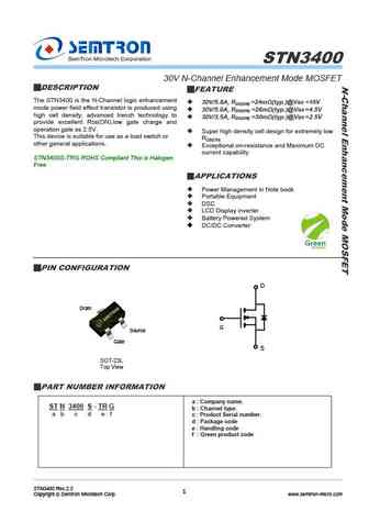
STN3400 30V N-Channel Enhancement Mode MOSFET DESCRIPTION FEATURE The STN3400 is the N-Channel logic enhancement 30V/5.8A, RDS(ON) =24m (typ.)@VGS =10V mode power field effect transistor is produced using 30V/5.0A, RDS(ON) =26m (typ.)@VGS =4.5V high cell density. advanced trench technology to 30V/3.5A, RDS(ON) =30m (typ.)@VGS =2.5V provide excellent RDS(
smc3400.pdf
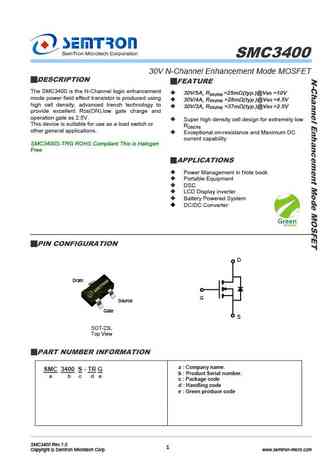
SMC3400 30V N-Channel Enhancement Mode MOSFET DESCRIPTION FEATURE The SMC3400 is the N-Channel logic enhancement 30V/5A, RDS(ON) =25m (typ.)@VGS =10V mode power field effect transistor is produced using 30V/4A, RDS(ON) =28m (typ.)@VGS =4.5V high cell density. advanced trench technology to 30V/3A, RDS(ON) =37m (typ.)@VGS =2.5V provide excellent RDS(ON).lo
sl3400.pdf
SL3400 N-Channel Power MOSFET D General Features VDS = 30V,ID = 5.8A G RDS(ON)
st3400s23rg.pdf
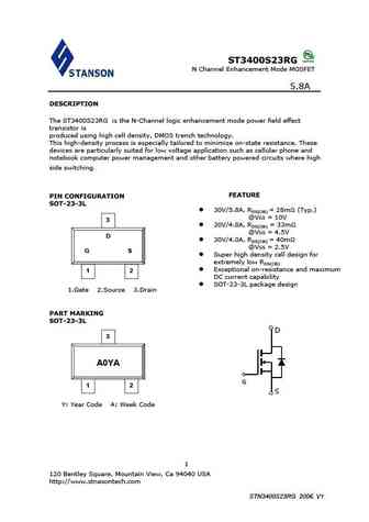
ST3400S23RG N Channel Enhancement Mode MOSFET 5.8A DESCRIPTION The ST3400S23RG is the N-Channel logic enhancement mode power field effect transistor is produced using high cell density, DMOS trench technology. This high-density process is especially tailored to minimize on-state resistance. These devices are particularly suited for low voltage application such as cellular phon
st3400srg.pdf
ST3400SRG N Channel Enhancement Mode MOSFET 5.8A DESCRIPTION The ST3400SRG is the N-Channel logic enhancement mode power field effect transistor is produced using high cell density, DMOS trench technology. This high-density process is especially tailored to minimize on-state resistance. These devices are particularly suited for low voltage application such as cellular phone and
ao3400a.pdf
R UMW UMW AO3400A UMW AO3400A N-Channel Enhancement Mode Features SOT 23 VDS (V) = 30V ID = 5.8 A (VGS = 10V) RDS(ON) 28m (VGS = 10V) RDS(ON) 33m (VGS = 4.5V) RDS(ON) 52m (VGS = 2.5V) 1. GATE 2. SOURCE 3. DRAIN Absolute Maximum Ratings Ta = 25 Parameter Symbol Rating Unit Drain-Source Voltage VDS 30 V Gate-Source Voltage VGS 12 V Continuous Drain Current TA=25 5.8 ID
atm3400ansa.pdf
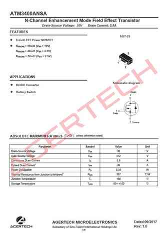
ATM3400ANSA N-Channel Enhancement Mode Field Effect Transistor Drain-Source Voltage 30V Drain Current 5.8A FEATURES SOT-23 Trench FET Power MOSFET R
atm3400nsa.pdf
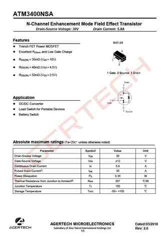
ATM3400NSA N-Channel Enhancement Mode Field Effect Transistor Drain-Source Voltage 30V Drain Current 5.8A Features Trench FET Power MOSFET Excellent R and Low Gate Charge DS(on) R
as3400.pdf
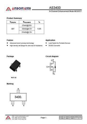
AS3400 N-Channel Enhancement Mode MOSFET Product Summary V(BR)DSS RDS(on)MAX ID 27m @10V 30V 33m @4.5V 5.6A 51m @2.5V Feature Application Advanced trench process technology Load Switch for Portable Devices High density cell design for ultra low on-resistance DC/DC Converter Package Circuit diagram SOT-23 Marking 3400. Document ID Issued Date Revised Date Revisio
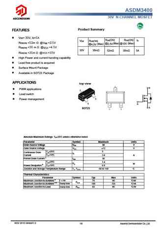
asdm3400za.pdf
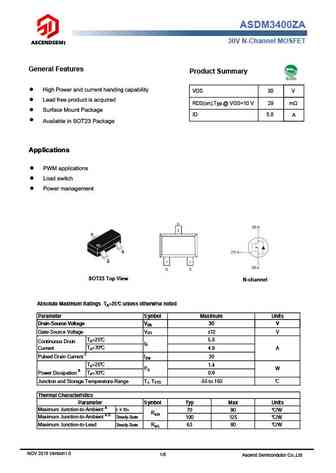
ASDM3400ZA 30V N-Channel MOSFET General Features Product Summary High Power and current handing capability VDS 30 V Lead free product is acquired RDS(on),Typ.@ VGS=10 V 29 m Surface Mount Package ID 5.8 A Available in SOT23 Package Applications PWM applications Load switch Power management SOT23 Top View N-channel Absolute Maximum Ratings TA=25
asdm3400zb.pdf

ASDM3400ZB 30V N-Channel MOSFET General Features Product Summary High Power and current handing capability VDS 30 V Lead free product is acquired RDS(on),Typ.@ VGS=10 V 29 m Surface Mount Package ID 5.8 A Available in SOT23-3 Package Applications PWM applications Load switch Power management SOT23-3 Top View N-channel Absolute Maximum Ratings T
asdm3400.pdf
ASDM3400 30V N-CHANNEL MOSFET Product Summary FEATURES V = 30V, I =5A DS D RDS(ON) RDS(ON) ID VDS RDS(ON) R
ao3400a.pdf
AO3400A MOSFET ROHS N-Channel Enhancement-Mode MOSFET SOT-23 - Features Advanced trench process technology High Density Cell Design For Ultra Low On-Resistance MAXIMUM RANTINGS Characteristic Symbol Max Unit Drain-Source Voltage BV 30 V DSS Gate- Source Voltage V +12 V GS Drain Current (continuous) 5.8 A I D Drain Current (pulsed) I 30 A DM Total Device Dissipat
ao3400.pdf
AO3400 N-Channel MOSFET Features Pin Configurations V = 30V DS I D = 5A R @V = 10V, TYP =35m DS(ON) GS R @V = 4.5V, TYP =40m DS(ON) GS General Description Advanced trench process technology High Density Cell Design For Ultra Low On-Resistance SOT-23 for Surface Mount Package. Absolute Maximum Ratings @T =25 unless otherwise noted A Characteri
ev3400.pdf
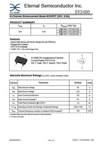
Eternal Semiconductor Inc. EV3400 N-Channel Enhancement-Mode MOSFET (30V, 5.8A) PRODUCT SUMMARY VDSS ID RDS(on) (m ) Typ. 25@ VGS = 10 V,ID=5.8A 30V 5.8A 36@ VGS = 4.5 V,ID=5.0A 40@ VGS = 2.5V,ID=4.0A Features Super high dense cell trench design for low RDS(on) Rugged and reliable SOT-23-3L package Lead Pb -free and halogen-free EV3400 Pin Assignment & Symb
ao3400.pdf
Plastic-Encapsulate Mosfets AO3400 FEATURES N-Channel MOSFET The AO3400 is the N-Channel logic enhancement mode power field effect transistor is produced using high cell density, DMOS trench technology. This high-density process is especially tailored to minimize on-state resistance. These devices are particularly suited for low voltage application such as cellular phone and notebook c
ao3400a.pdf
AO3400A N-Ch 30V Fast Switching MOSFETs Description Product Summary The AO3400A is the high cell density trenched N- VDS 30 V ch MOSFETs, which provides excellent RDSON and efficiency for most of the small power switching RDS(ON),typ 27 m and load switch applications. ID 5.2 A The AO3400A meet the RoHS and Green Product requirement with full function reliability approve
hss3400a.pdf
HSS3400A Description Product Summary VDS 30 V The HSS3400A is the high cell density trenched N- ch MOSFETs, which provides excellent RDSON RDS(ON),max 26 m and efficiency for most of the small power switching and load switch applications. ID 5.5 A The HSS3400A meet the RoHS and Green Product requirement with full function reliability approved. l Green Device Available
hx3400.pdf
SOT-23-3 Plastic-Encapsulate Transistors HX3400 MOSFET(N-Channel) FEATURES High Power and current handing capability Lead free product is acquired Surface Mout Package MARKING XORB MAXIMUM RATINGS (TA=25 unless otherwise noted) Symbol Parameter Value Units VDS Drain-Source voltage 30 V VGS Gate-Source voltage 12 V ID Drain current 5.8 A PD Power Dissipation 1.4 W
hx3400a.pdf
SOT-23-3 Plastic-Encapsulate Transistors HX3400AMOSFET(N-Channel) FEATURES TrenchFET Power MOSFET Load Switch for Portable Devices DC/DC Converter MARKING A09T MAXIMUM RATINGS (TA=25 unless otherwise noted) Symbol Parameter Value Units VDS Drain-Source voltage 20 V VGS Gate-Source voltage 8 V ID Drain current 3.6 A PD Power Dissipation 1 W Tj Junction Temperature 150 Ts
jmtl3400l.pdf
JMTL3400L Description JMT N-channel Enhancement Mode Power MosFET Features Applications 30V, 5A Load Switch RDS(ON)
jmtv3400a.pdf
JMTV3400A Description JMT N-channel Enhancement Mode Power MOSFET Features Applications 30V, 8A Load Switch RDS(ON)
jmtl3400a.pdf
JMTL3400A Description JMT N-channel Enhancement Mode Power MOSFET Features Applications 30V, 5.8A Load Switch RDS(ON)
jmtq3400d.pdf
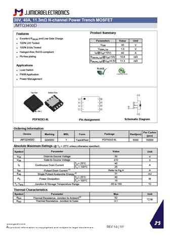
30V, 40A, 11.3m N-channel Power Trench MOSFET JMTQ3400D Product Summary Features Excellent RDS(ON) and Low Gate Charge Parameters Value Unit 100% UIS Tested VDSS 30 V 100% Vds Tested VGS(th)_Typ 1.0 V Halogen-free; RoHS-compliant ID(@VGS=10V) 40 A Pb-free plating RDS(ON)_Typ(@VGS=10V 10.6 mW RDS(ON)_Typ(@VGS=4.5V 11.3 mW Applications Load Switch
jmtj3400a.pdf
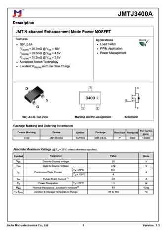
JMTJ3400A Description JMT N-channel Enhancement Mode Power MOSFET Features Applications 30V, 5.8A Load Switch RDS(ON)
jst3400.pdf
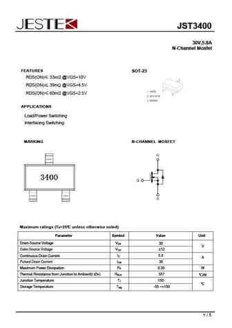
JST3400 30V,5.8A N-Channel Mosfet FEATURES SOT-23 RDS(ON) 33m @VGS=10V RDS(ON) 39m @VGS=4.5V RDS(ON) 60m @VGS=2.5V APPLICATIONS Load/Power Switching Interfacing Switching MARKING N-CHANNEL MOSFET Maximum ratings (Ta=25 unless otherwise noted) Parameter Symbol Value Unit Drain-Source Voltage VDS 30 V Gate-Source Voltage V 12 GS I 5.8 D Continuous Drain
jsm3400.pdf
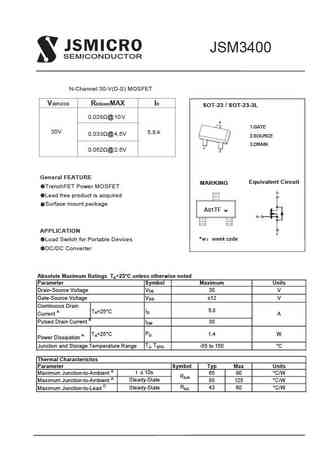
JSM3400 N-Channel 30-V(D-S) MOSFET V(BR)DSS RDS(on)MAX ID SOT-23 SOT-23-3L / 0.028 @ 10V 3 1.GATE 30V 5.8A 0.033 @ 4.5V 2.SOURCE 3.DRAIN 1 0.052 @ 2.5V 2 General FEATURE Equivalent Circuit MARKING TrenchFET Power MOSFET Lead free product is acquired Surface mount package A01TF w APPLICATION *w week code Load Switch for Portable Devices DC/DC Convert
lpm3400b3f.pdf
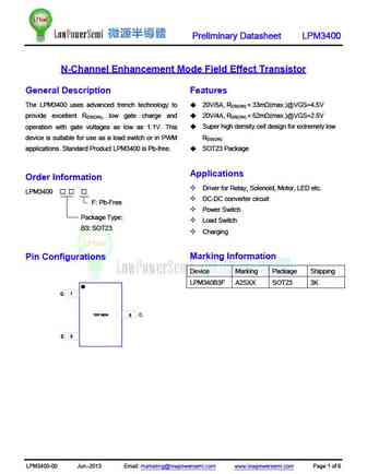
Preliminary Datasheet LPM3400 N-Channel Enhancement Mode Field Effect Transistor General Description Features The LPM3400 uses advanced trench technology to 20V/5A, R 33m (max.)@VGS=4.5V DS(ON) provide excellent R , low gate charge and 20V/4A, R 52m (max.)@VGS=2.5V DS(ON) DS(ON) operation with gate voltages as low as 1.1V. This Super high density cell design for
lnsc3400.pdf
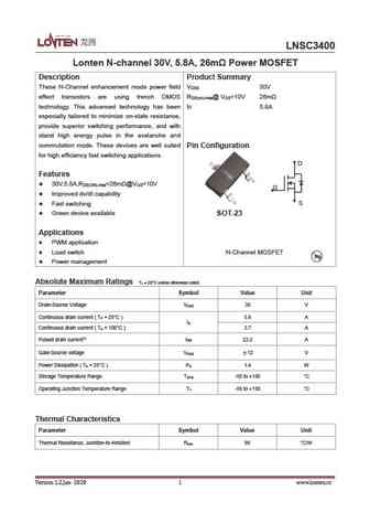
LNSC3400 Lonten N-channel 30V, 5.8A, 26m Power MOSFET Description Product Summary These N-Channel enhancement mode power field V 30V DSS effect transistors are using trench DMOS R DS(on).max@ V =10V 26m GS technology. This advanced technology has been I 5.8A D especially tailored to minimize on-state resistance, provide superior switching performance, and with stand high energy
lnsa3400.pdf
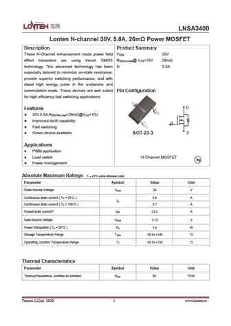
LNSA3400 Lonten N-channel 30V, 5.8A, 26m Power MOSFET Description Product Summary These N-Channel enhancement mode power field V 30V DSS effect transistors are using trench DMOS R DS(on).max@ V =10V 26m GS technology. This advanced technology has been I 5.8A D especially tailored to minimize on-state resistance, provide superior switching performance, and with stand high energy
ao3400mi-ms.pdf
www.msksemi.com AO3400MI-MS Semiconductor Compiance SOT-23 FEATURE High dense cell design for extremely low R DS(ON) Exceptional on-resistance and maximum DC current capability 1. GATE 2. SOURCE APPLICATION 3. DRAIN Load/Power Switching Interfacing Switching Equivalent Circuit I V(BR)DSS RDS(on)MAX D 35m @ 10V 40m @4.5V 30 V 5.8A 52m @2.5V Maximum ratin
si3400.pdf
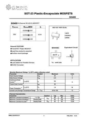
SOT-23 Plastic-Encapsulate MOSFETS SI3400 N-Channel 30-V(D-S) MOSFET SI3400 V(BR)DSS RDS(on)MAX ID SOT-23 SOT-23-3L / 0.028 @ 10V 3 1.GATE 30V 5.8A 0.033 @ 4.5V 2.SOURCE 3.DRAIN 1 0.052 @ 2.5V 2 General FEATURE Equivalent Circuit MARKING TrenchFET Power MOSFET Lead free product is acquired Surface mount package A01TF w APPLICATION *w week code Load Sw
ps3400n.pdf
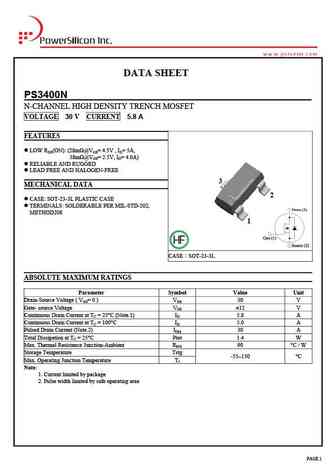
DATA SHEET PS3400N N-CHANNEL HIGH DENSITY TRENCH MOSFET VOLTAGE 30 V CURRENT 5.8 A FEATURES LOW RDS(ON) (28m @VGS= 4.5V , ID= 5A, 38m @VGS= 2.5V, ID= 4.0A) RELIABLE AND RUGGED LEAD FREE AND HALOGEN-FREE 3 MECHANICAL DATA 2 CASE SOT-23-3L PLASTIC CASE TERMINALS SOLDERABLE PER MIL-STD-202, METHOD208 1 CASE SOT-23-3L ABSOLUTE MAXIMUM R
pjm3400nsa.pdf
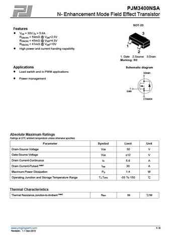
PJM3400NSA N- Enhancement Mode Field Effect Transistor SOT-23 Features VDS = 30V,ID = 5.8A RDS(ON)
pjm3400nsc.pdf
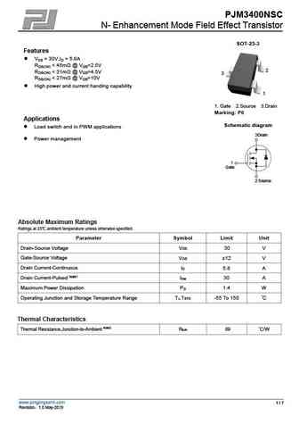
PJM3400NSC N- Enhancement Mode Field Effect Transistor SOT-23-3 Features VDS = 30V,ID = 5.8A RDS(ON)
sr3400.pdf
Leading Circuit Protection SR3400 Products and Solutions 30V N-Channel MOSFET Product Summary SOT-23 V R I (BR)DSS DS(on)MAX D 35m @10V 30V 40m @4.5V 5.8A 52m @2.5V Feature TrenchFET Power MOSFET Schematic diagram Excellent RDS(on) and Low Gate Charge Application DC/DC Converter Load Switch for Portable Devices Battery Switch MARKING ABSOLUTE MAXIMUM
ao3400.pdf
AO3400 30V N-Channel Enhancement Mode MOSFET VDS= 30V RDS(ON), Vgs@10V, Ids@5.8A
agm3400el.pdf
AGM3400EL Table 3. Electrical Characteristics (TJ=25 unless otherwise noted) Symbol Parameter Conditions Min Typ Max Unit On/Off States BV Drain-Source Breakdown Voltage V =0V I =250 A 30 -- -- V GS D DSS Zero Gate Voltage Drain Current V =30V,V =0V -- -- 1 A DS GS I DSS V = 12V,V =0V -- -- nA GS DS IGSS Gate-Body Leakage Current 100 VGS(th) Gate Threshold Voltage V
agm3400e.pdf
AGM3400E Typical Performance Characteristics Figure1. Output Characteristics Figure2. Transfer Characteristics Figure 3 On-Resistance vs. Drain Current Figure 4 On-Resistance vs. Junction Temperature and Gate Voltage Figure5. Capacitance Characteristics Figure6. Gate Charge www.agm-mos.com 3 VER2.71 AGM3400E Figure7. Safe Operation Area Figure8. Maximum Continuous Drain
ao3400.pdf
N-Channel Enhancement Mode MOSFET Feature SC-59 30V/5.8A, RDS(ON) = 35m (MAX) @VGS = 10V. 3 RDS(ON) =40m (MAX) @VGS = 4.5V. RDS(ON) =55m (MAX) @VGS = 2.5V. Super High dense cell design for extremely low RDS(ON) . 2 Reliable and Rugged. 1 SC-59 for Surface Mount Package. Applications 1 Gate 2 Source 3 Drain Power Management Portable Equipment and
wtm3400.pdf
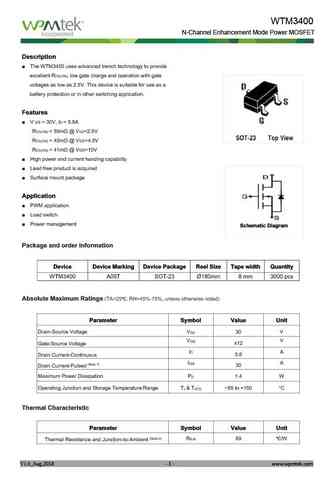
WTM3400 N-Channel Enhancement Mode Power MOSFET Description The WTM3400 uses advanced trench technology to provide excellent R , low gate charge and operation with gate DS(ON) voltages as low as 2.5V. This device is suitable for use as a battery protection or in other switching application. Features V DS = 30V, lD = 5.8A R
ao3400.pdf
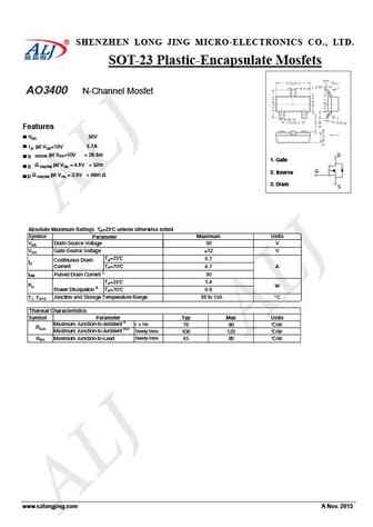
SHENZHEN LONG JING MICRO-ELECTRONICS CO., LTD. SOT-23 Plastic-Encapsulate Mosfets AO3400 N-Channel Mosfet Features 30V VDS 5.7A I (at VGS=10V D (at VGS=10V
tf3400.pdf
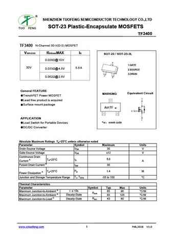
SHENZHEN TUOFENG SEMICONDUCTOR TECHNOLOGY CO.,LTD SOT-23 Plastic-Encapsulate MOSFETS 3400 TF N-Channel 30-V(D-S) MOSFET TF3400 V(BR)DSS RDS(on)MAX ID SOT-23 SOT-23-3L / 0.028 @ 10V 3 1.GATE 30V 5.8A 0.033 @ 4.5V 2.SOURCE 3.DRAIN 1 0.052 @ 2.5V 2 General FEATURE Equivalent Circuit MARKING TrenchFET Power MOSFET Lead free product is acquired Surface mount pack
ao3400.pdf
AO3400 AO3400 AO3400 AO3400 SI2305 SOT-23 Plastic-Encapsulate MOSFETS N-Channel Enhancement Mode Field Effect Transistor N-Channel Enhancement Mode Field Effect Transistor N-Channel Enhancement Mode Field Effect Transistor N-Channel Enhancement Mode Field Effect Transistor AO3400 AO3400 AO3400 AO3400 AO3400 FEATURE High dense cell design for extremely low RDS(ON) Excepti
wst3400.pdf
WST3400 N-Ch MOSFET General Description Product Summery The WST3400 is the highest performance trench BVDSS RDSON ID N-Ch MOSFET with extreme high cell density , which provide excellent RDSON and gate charge 30V 18m 7A for most of the small power switching and load switch applications. Applications The WST3400 meet the RoHS and Green Product requirement with full functio
wst3400s.pdf
WST3400S N-Ch MOSFET General Description Product Summery The WST3400S is the highest performance BVDSS RDSON ID trench N-Ch MOSFET with extreme high cell density , which provide excellent RDSON and 30V 27m 5.6A gate charge for most of the small power switching and load switch applications. Applications The WST3400S meet the RoHS and Green Product requirement with full fu
wst3400a.pdf
WST3400A N-Ch MOSFET General Description Product Summery The WST3400A is the highest performance BVDSS RDSON ID trench N-Ch MOSFET with extreme high cell density , which provide excellent RDSON and 30V 20m 6.4A gate charge for most of the small power switching and load switch applications. Applications The WST3400A meet the RoHS and Green Product requirement with full fu
sm3400.pdf
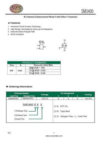
SM3400 N-Channel Enhancement Mode Field Effect Transistor P-Channel Enhancement-Mode MOSFET Features 1 Advanced Trench Process Technology. 2 High Density Cell Design for Ultra Low On-Resistance. 3 Improved Shoot-Through FOM 4 RoHS Compliant D SOT-23 Top View G D S G S PRODUCT SUMMARY VDSS ID RDS(on) (m-ohm) Max 28@ VGS = 10V 33 @ VGS = 4.5V 30V 5.8A
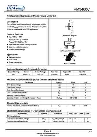
hm3400pr.pdf
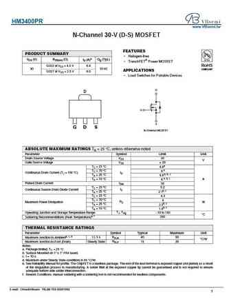
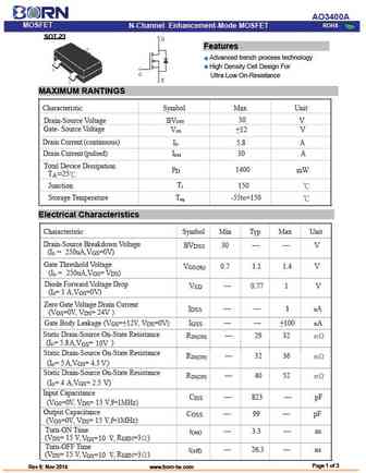
HM3400PR www.VBsemi.tw N-Channel 30-V (D-S) MOSFET FEATURES PRODUCT SUMMARY Halogen-free VDS (V) RDS(on) ( ) ID (A)a Qg (Typ.) TrenchFET Power MOSFET 0.022 at VGS = 4.5 V 6.8 RoHS 30 10 nC COMPLIANT APPLICATIONS 0.027 at VGS = 2.5 V 6.0 Load Switches for Portable Devices D D G S G D S N-Channel MOSFET ABSOLUTE MAXIMUM RATINGS TA = 25 C, unless otherwise n
spn3400s23rg.pdf
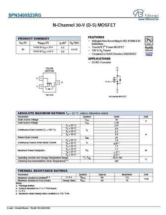
SPN3400S23RG www.VBsemi.tw N-Channel 30-V (D-S) MOSFET FEATURES PRODUCT SUMMARY Halogen-free According to IEC 61249-2-21 VDS (V) RDS(on) ( ) ID (A)a Qg (Typ.) Definition 0.030 at VGS = 10 V TrenchFET Power MOSFET 6.5 30 4.5 nC 100 % Rg Tested 0.033 at VGS = 4.5 V 6.0 Compliant to RoHS Directive 2002/95/EC APPLICATIONS DC/DC Converter D TO-236 (SOT-23
kd3400srg.pdf
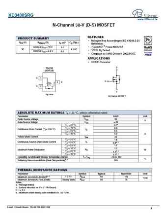
KD3400SRG www.VBsemi.tw N-Channel 30-V (D-S) MOSFET FEATURES PRODUCT SUMMARY Halogen-free According to IEC 61249-2-21 VDS (V) RDS(on) ( ) ID (A)a Qg (Typ.) Definition 0.030 at VGS = 10 V TrenchFET Power MOSFET 6.5 30 4.5 nC 100 % Rg Tested 0.033 at VGS = 4.5 V 6.0 Compliant to RoHS Directive 2002/95/EC APPLICATIONS DC/DC Converter D TO-236 (SOT-23)
cj3400.pdf

CJ3400 www.VBsemi.tw N-Channel 30-V (D-S) MOSFET FEATURES PRODUCT SUMMARY Halogen-free According to IEC 61249-2-21 VDS (V) RDS(on) ( ) ID (A)a Qg (Typ.) Definition 0.030 at VGS = 10 V TrenchFET Power MOSFET 6.5 30 4.5 nC 100 % Rg Tested 0.033 at VGS = 4.5 V 6.0 Compliant to RoHS Directive 2002/95/EC APPLICATIONS DC/DC Converter D TO-236 (SOT-23) G 1
nce3400a.pdf
NCE3400A www.VBsemi.tw N-Channel 30-V (D-S) MOSFET FEATURES PRODUCT SUMMARY Halogen-free According to IEC 61249-2-21 VDS (V) RDS(on) ( ) ID (A)a Qg (Typ.) Definition 0.030 at VGS = 10 V TrenchFET Power MOSFET 6.5 30 4.5 nC 100 % Rg Tested 0.033 at VGS = 4.5 V 6.0 Compliant to RoHS Directive 2002/95/EC APPLICATIONS DC/DC Converter D TO-236 (SOT-23) G
ao3400.pdf
AO3400 www.VBsemi.tw N-Channel 30-V (D-S) MOSFET FEATURES PRODUCT SUMMARY Halogen-free According to IEC 61249-2-21 VDS (V) RDS(on) ( ) ID (A)a Qg (Typ.) Definition 0.030 at VGS = 10 V TrenchFET Power MOSFET 6.5 30 4.5 nC 100 % Rg Tested 0.033 at VGS = 4.5 V 6.0 Compliant to RoHS Directive 2002/95/EC APPLICATIONS DC/DC Converter D TO-236 (SOT-23) G 1
yjl3400a.pdf
RoHS COMPLIANT YJL3400A N-Channel Enhancement Mode Field Effect Transistor Product Summary V 30V DS I 5.6A D R ( at V =10V) 27 mohm DS(ON) GS R ( at V =4.5V) 33 mohm DS(ON) GS R ( at V =2.5V) 51 mohm DS(ON) GS General Description Trench Power LV MOSFET technology High density cell design for low R DS(ON) High Speed switch
yjq3400a.pdf
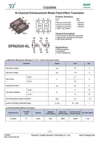
RoHS COMPLIANT YJQ3400A N-Channel Enhancement Mode Field Effect Transistor Product Summary V 30V DS I 7.7A D R ( at V =10V) 23mohm DS(ON) GS R ( at V =4.5V) 29mohm DS(ON) GS R ( at V =2.5V) 43mohm DS(ON) GS 100% V Tested DS General Description Trench Power LV MOSFET technology High density cell design for low R DS(ON
hm3400 sot23-3l.pdf

HM3400 N-Channel Enhancement Mode Power MOSFET DESCRIPTION The HM3400 uses advanced trench technology to provide D excellent RDS(ON), low gate charge and operation with gate voltages as low as 2.5V. This device is suitable for use as a G Battery protection or in other Switching application. S GENERAL FEATURES VDS = 30V,ID = 5.8A Schematic diagram RDS(ON)
hm3400c.pdf
N-Channel Enhancement Mode Power MOSFET D Description The uses advanced trench technology to provide G excellent RDS(ON) and low gate charge .This device is suitable for use as a load switch or in PWM applications. S General Features Schematic diagram VDS = 30V,ID = 3.6A RDS(ON)
hm3400dr.pdf
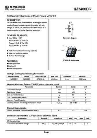
HM3400DR N-Channel Enhancement Mode Power MOSFET DESCRIPTION The HM3400DR uses advanced trench technology to provide D excellent RDS(ON), low gate charge and operation with gate voltages as low as 2.5V. This device is suitable for use as a G Battery protection or in other Switching application. S GENERAL FEATURES VDS = 30V,ID = 8 A Schematic diagram RDS(ON)
hm3400d.pdf
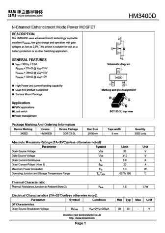
HM3400D N-Channel Enhancement Mode Power MOSFET DESCRIPTION The HM3400D uses advanced trench technology to provide D excellent RDS(ON), low gate charge and operation with gate voltages as low as 2.5V. This device is suitable for use as a G Battery protection or in other Switching application. S GENERAL FEATURES VDS = 30V,ID = 5.0A Schematic diagram RDS(ON)
hm3400b.pdf

3400 N-Channel Enhancement Mode Power MOSFET DESCRIPTION The 3400 uses advanced trench technology to provide D excellent RDS(ON), low gate charge and operation with gate voltages as low as 2.5V. This device is suitable for use as a G Battery protection or in other Switching application. S GENERAL FEATURES VDS = 30V,ID = 5.8A Schematic diagram RDS(ON)
ao3400s.pdf
Description The AO3400S combines advanced trench technology to provide excellent RDS(ON), low gate charge and operation with gate voltage as low as 2.5V. This device is suitable for use as a load switch or other general applications. Features VDS=30V, ID=5.1A RDS(ON)
cm3400.pdf
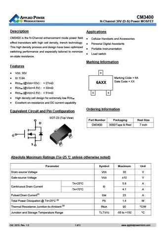
CM3400 N-Channel 30V (D-S) Power MOSFET Description Applications CM3400 is the N-Channel enhancement mode power field Cellular Handsets and Accessories effect transistors with high cell density, trench technology. Personal Digital Assistants This high density process and design have been optimized Portable Instrumentation switching performance and especially tai
pm3400.pdf
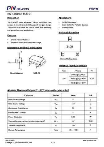
PM3400 30V N-Channel MOSFET Description Applications The PM3400 uses advanced Trench technology and DC/DC Converter designs to provide excellent R with low gate charge. Load Switch for Portable Devices DS(ON) This device is suitable for use in PWM, load switching Battery Switch and general purpose applications. Marking Information Features Trench Power MOSFET
ap3400mi-l.pdf
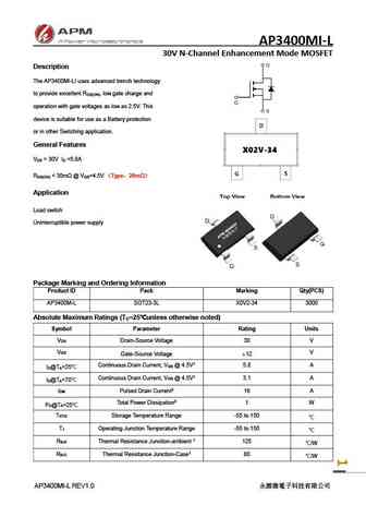
AP3400MI-L 30V N-Channel Enhancement Mode MOSFET Description The AP3400MI-LI uses advanced trench technology to provide excellent R , low gate charge and DS(ON) operation with gate voltages as low as 2.5V. This device is suitable for use as a Battery protection or in other Switching application. General Features V = 30V I =5.8A DS D R
ap3400bi.pdf
AP3400BI 30V N-Channel Enhancement Mode MOSFET Description The AP3400BI uses advanced trench technology to provide excellent R , low gate charge and DS(ON) operation with gate voltages as low as 2.5V. This device is suitable for use as a Battery protection or in other Switching application. General Features V = 30V I =5.8A DS D R
ap3400di.pdf
AP3400DI 20V N-Channel Enhancement Mode MOSFET Description The AP3400DI uses advanced trench technology to provide excellent R , low gate charge and DS(ON) operation with gate voltages as low as 2.5V. This device is suitable for use as a Battery protection or in other Switching application. General Features V = 20V I =3.2A DS D R
ap3400ai.pdf
AP3400AI 30V N-Channel Enhancement Mode MOSFET Description The AP3400AI uses advanced trench technology to provide excellent R , low gate charge and DS(ON) operation with gate voltages as low as 2.5V. This device is suitable for use as a Battery protection or in other Switching application. General Features V = 30V I =5.8A DS D R
ap3400ci.pdf
AP3400CI 30V N-Channel Enhancement Mode MOSFET Description The AP3400CI uses advanced trench technology to provide excellent R , low gate charge and DS(ON) operation with gate voltages as low as 2.5V. This device is suitable for use as a Battery protection or in other Switching application. General Features V = 30V I =4.2A DS D R
ap3400mi.pdf
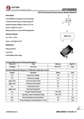
AP3400MI 30V N-Channel Enhancement Mode MOSFET Description The AP3400MI uses advanced trench technology to provide excellent R , low gate charge and DS(ON) operation with gate voltages as low as 2.5V. This device is suitable for use as a Battery protection or in other Switching application. General Features V = 30V I =5.8A DS D R
Другие IGBT... 1002, 1115, 1515, G1601, 2300, 2301, 2302, 3035, IRF9640, 3401, 3415, 6616, 6703, 6760, 7080, 8070, 8680
Параметры MOSFET. Взаимосвязь и компромиссы
🌐 : EN ES РУ

Список транзисторов
Обновления
MOSFET: BC2301 | BC1012W | BC1012T | BC1012 | 2SK3019WT | 2SK3019W | 2SK3018WT | CS95118 | CS85105A | CS75N45 | CS72N12 | CS55N50 | CS48N75A | CS40N27 | MSQ60P04D | MSQ40P07D
Popular searches
2sa1011 | 2sa1283 | 2sb646 | 2sc1885 datasheet | 2sc2580 | 2sc710 | 2sc968 | 2sd217