G23. Аналоги и основные параметры
Наименование производителя: G23
Тип транзистора: MOSFET
Полярность: P
Предельные значения
Pd ⓘ - Максимальная рассеиваемая мощность: 1.7 W
|Vds|ⓘ - Максимально допустимое напряжение сток-исток: 18 V
|Vgs|ⓘ - Максимально допустимое напряжение затвор-исток: 12 V
|Id| ⓘ - Максимально допустимый постоянный ток стока: 6 A
Tj ⓘ - Максимальная температура канала: 150 °C
Электрические характеристики
tr ⓘ - Время нарастания: 35 ns
Cossⓘ - Выходная емкость: 290 pf
RDSonⓘ - Сопротивление сток-исток открытого транзистора: 0.035 Ohm
Тип корпуса: SOT23
Аналог (замена) для G23
- подборⓘ MOSFET транзистора по параметрам
G23 даташит
g23.pdf
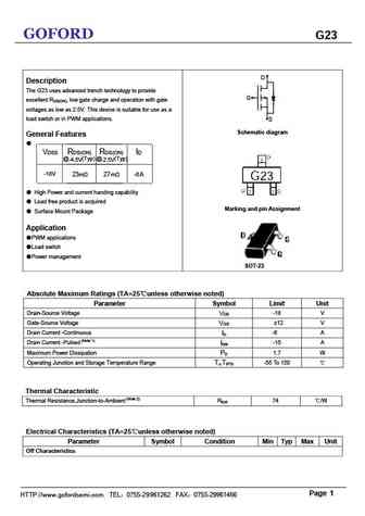
GOFORD G23 D Description The G23 uses advanced trench technology to provide G excellent RDS(ON), low gate charge and operation with gate voltages as low as 2.5V. This device is suitable for use as a load switch or in PWM applications. S Schematic diagram General Features VDSS RDS(ON) RDS(ON) ID (Typ) @-2.5V @-4.5V (Typ) -18V 23m 27m -6 A G23 High Pow
bls7g2325l-105.pdf
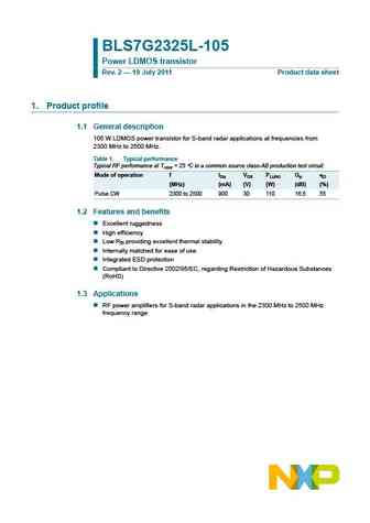
BLS7G2325L-105 Power LDMOS transistor Rev. 2 19 July 2011 Product data sheet 1. Product profile 1.1 General description 105 W LDMOS power transistor for S-band radar applications at frequencies from 2300 MHz to 2500 MHz. Table 1. Typical performance Typical RF performance at Tcase = 25 C in a common source class-AB production test circuit. Mode of operation f IDq VDS PL(AV) Gp
bfg235.pdf
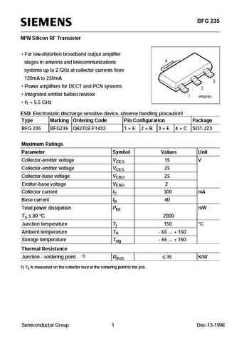
BFG 235 NPN Silicon RF Transistor For low-distortion broadband output amplifier stages in antenna and telecommunications systems up to 2 GHz at collector currents from 120mA to 250mA Power amplifiers for DECT and PCN systems Integrated emitter ballast resistor fT = 5.5 GHz ESD Electrostatic discharge sensitive device, observe handling precaution! Type Marking Order
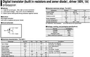
dtdg23yp.pdf
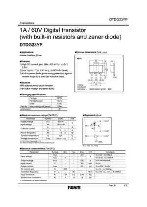
DTDG23YP Transistors 1A / 60V Digital transistor (with built-in resistors and zener diode) DTDG23YP Applications External dimensions (Unit mm) Inverter, Interface, Driver MPT3 4.5 1.5 Features 1.6 1) High DC current gain. (Min. 300 at VO / IO=2V / 0.5A) 2) Low Vo(on). (Typ. 0.4V at IO / II=500mA / 5mA) (1) (2) (3) 3) Built-in zener diode gives strong protection aga
sihg23n60e.pdf
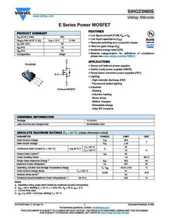
SiHG23N60E www.vishay.com Vishay Siliconix E Series Power MOSFET FEATURES PRODUCT SUMMARY Low figure-of-merit (FOM) Ron x Qg VDS (V) at TJ max. 650 Low input capacitance (Ciss) RDS(on) max. at 25 C ( ) VGS = 10 V 0.158 Reduced switching and conduction losses Qg max. (nC) 95 Ultra low gate charge (Qg) Qgs (nC) 16 Avalanche energy rated (UIS) Qgd (nC) 25
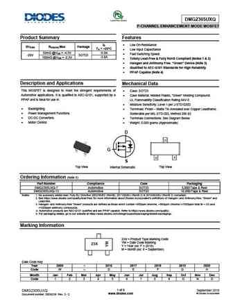
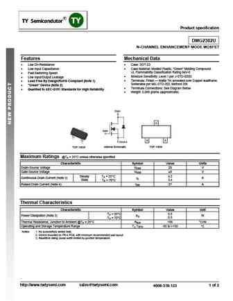
dmg2302uq.pdf
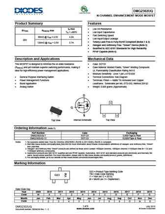
DMG2302UQ N-CHANNEL ENHANCEMENT MODE MOSFET Product Summary Features Low On-Resistance ID max BVDSS RDS(ON) max TA = +25 C Low Input Capacitance Fast Switching Speed 90m @ VGS = 4.5V 4.2A Low Input/Output Leakage 20V Totally Lead-Free & Fully RoHS Compliant (Notes 1 & 2) 120m @ VGS = 2.5V 2.7A Halogen and Antimony Free. Green Device
dmg2301lk.pdf
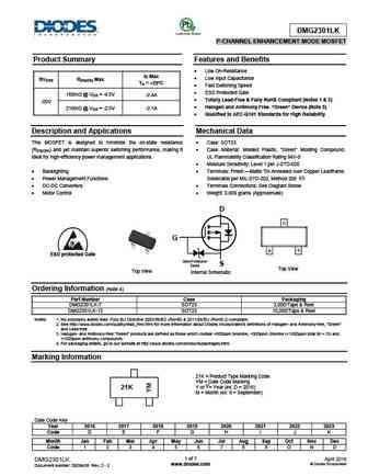
DMG2301LK P-CHANNEL ENHANCEMENT MODE MOSFET Product Summary Features and Benefits Low On-Resistance ID Max Low Input Capacitance BVDSS RDS(ON) Max TA = +25 C Fast Switching Speed ESD Protected Gate 160m @ VGS = -4.5V -2.4A Totally Lead-Free & Fully RoHS Compliant (Notes 1 & 2) -20V Halogen and Antimony Free. Green Device (Note 3) 210
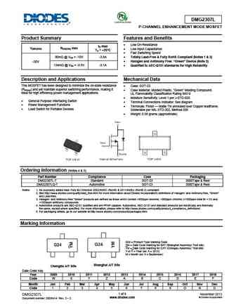
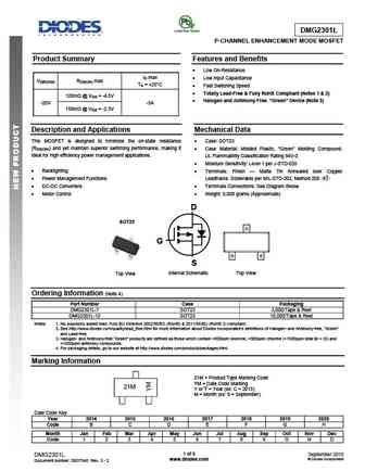
dmg2301u.pdf
DMG2301U P-CHANNEL ENHANCEMENT MODE MOSFET Please click here to visit our online spice models database. Features Mechanical Data Low On-Resistance Case SOT-23 Low Input Capacitance Case Material Molded Plastic, Green Molding Compound. UL Flammability Classification Rating 94V-0 Fast Switching Speed Moisture Sensitivity Level 1 per J-STD-020D L
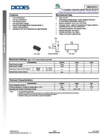
dmg2307l.pdf
DMG2307L P-CHANNEL ENHANCEMENT MODE MOSFET Product Summary Features and Benefits Low On-Resistance ID max V(BR)DSS RDS(ON) max Low Input Capacitance TA = +25 C Fast Switching Speed 90m @ VGS = -10V -3.8A Totally Lead-Free & Fully RoHS Compliant (Notes 1 & 2) Halogen and Antimony Free. Green Device (Note 3) -30V 134m @ VGS = -4.5V -3.1A
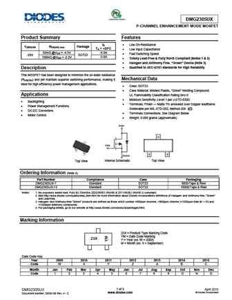
dmg2305uxq.pdf
DMG2305UXQ P-CHANNEL ENHANCEMENT MODE MOSFET Product Summary Features ID Low On-Resistance BVDSS RDS(ON) Max Package TA = +25 C Low Input Capacitance 52m @VGS = -4.5V -5.0A Fast Switching Speed -20V SOT23 -3.6A 100m @VGS = -2.5V Totally Lead-Free & Fully RoHS Compliant (Notes 1 & 2) Halogen and Antimony Free. Green Device (Note 3)
dmg2302uk.pdf
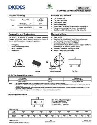
DMG2302UK N-CHANNEL ENHANCEMENT MODE MOSFET Product Summary Features and Benefits Low On-Resistance ID Max V(BR)DSS RDS(ON) Max Low Input Capacitance TA = +25 C Fast Switching Speed 90m @ VGS = 4.5V 2.8A ESD Protected Gate 20V Totally Lead-Free & Fully RoHS Compliant (Notes 1 & 2) 120m @ VGS = 2.5V 2.4A Halogen and Antimony Free. Gre
dmg2301l.pdf
DMG2301L P-CHANNEL ENHANCEMENT MODE MOSFET Product Summary Features and Benefits Low On-Resistance ID max Low Input Capacitance V(BR)DSS RDS(ON) max TA = +25 C Fast Switching Speed Totally Lead-Free & Fully RoHS Compliant (Notes 1 & 2) 120m @ VGS = -4.5V Halogen and Antimony Free. Green Device (Note 3) -20V -3A 150m @ VGS = -2.5V De
dmg2302u.pdf
DMG2302U N-CHANNEL ENHANCEMENT MODE MOSFET Please click here to visit our online spice models database. Features Mechanical Data Low On-Resistance Case SOT-23 Low Input Capacitance Case Material Molded Plastic, Green Molding Compound. UL Flammability Classification Rating 94V-0 Fast Switching Speed Moisture Sensitivity Level 1 per J-STD-020D L
g233.pdf
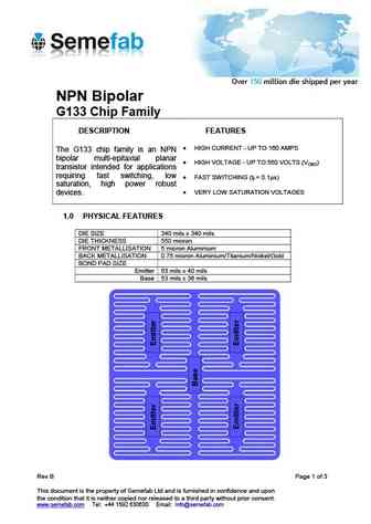
Over 150 million die shipped per year NPN Bipolar G133 Chip Family DESCRIPTION FEATURES HIGH CURRENT - UP TO 160 AMPS The G133 chip family is an NPN bipolar multi-epitaxial planar HIGH VOLTAGE - UP TO 550 VOLTS (VCBO) transistor intended for applications requiring fast switching, low FAST SWITCHING (tf = 0.1 s) saturation, high power robust VERY LOW SAT
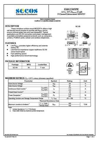
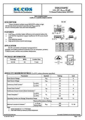
smg2343pe.pdf
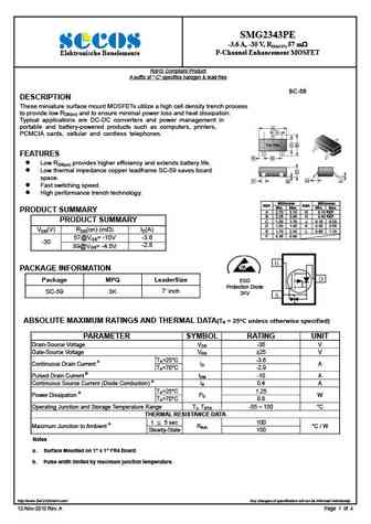
SMG2343PE -3.6 A, -30 V, RDS(ON) 57 m P-Channel Enhancement MOSFET Elektronische Bauelemente RoHS Compliant Product A suffix of -C specifies halogen & lead-free SC-59 DESCRIPTION These miniature surface mount MOSFETs utilize a high cell density trench process to provide low RDS(on) and to ensure minimal power loss and heat dissipation. Typical applications are DC-DC
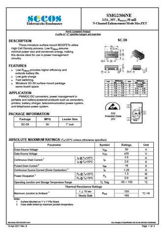
smg2334n.pdf
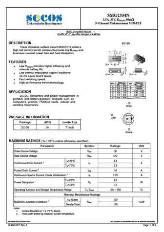
SMG2334N 3.5A, 30V, RDS(ON) 60m N-Channel Enhancement MOSFET Elektronische Bauelemente RoHS Compliant Product A suffix of -C specifies halogen & lead-free DESCRIPTION SC-59 These miniature surface mount MOSFETs utilize a high cell density trench process to provide low RDS(on) and A L to ensure minimal power loss and heat dissipation. 3 3 Top View C B 1 1 2
smg2327p.pdf
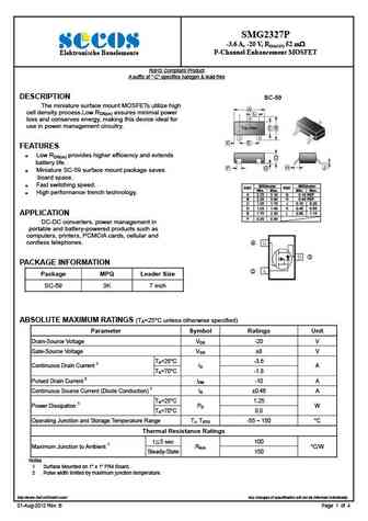
SMG2327P -3.6 A, -20 V, RDS(ON) 52 m P-Channel Enhancement MOSFET Elektronische Bauelemente RoHS Compliant Product A suffix of -C specifies halogen & lead-free DESCRIPTION SC-59 The miniature surface mount MOSFETs utilize high A cell density process.Low RDS(on) assures minimal power L 3 loss and conserves energy, making this device ideal for 3 use in power man
smg2305.pdf
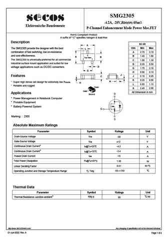
SMG2305 -4.2A, -20V,RDS(ON) 65m Elektronische Bauelemente P-Channel Enhancement Mode Power Mos.FET RoHS Compliant Product A suffix of -C specifies halogen & lead-free Description SC-59 A Dim Min Max The SMG2305 provide the designer with the best L combination of fast switching, low on-resistance A 2.70 3.10 3 and cost-effectiveness. B 1.40 1.60 S B Top View 2 1
smg2343p.pdf

SMG2343P -3.6 A, -30 V, RDS(ON) 0.057 P-Channel Enhancement MOSFET Elektronische Bauelemente RoHS Compliant Product A suffix of -C specifies halogen & lead-free SC-59 DESCRIPTION The miniature surface mount MOSFETs utilize a high cell density trench process To provide low RDS(on) and to ensure minimal power loss and heat dissipation. Typical applications are DC-DC
smg2321p.pdf
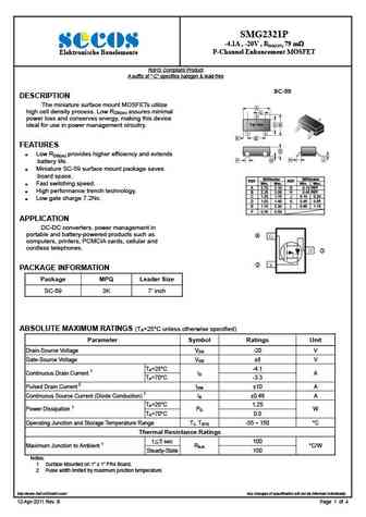
SMG2321P -4.1A , -20V , RDS(ON) 79 m P-Channel Enhancement MOSFET Elektronische Bauelemente RoHS Compliant Product A suffix of -C specifies halogen & lead-free SC-59 DESCRIPTION The miniature surface mount MOSFETs utilize A high cell density process. Low RDS(on) assures minimal L 3 power loss and conserves energy, making this device 3 Top View C B ideal for use
smg2302.pdf
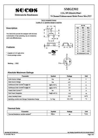
SMG2302 3.2A, 20V,RDS(ON) 85m Elektronische Bauelemente N-Channel Enhancement Mode Power Mos.FET RoHS Compliant Product A suffix of "-C" specifies halogen & lead-free SC-59 A Dim Min Max Description L A 2.70 3.10 3 B 1.40 1.60 S B Top View The SMG2302 provide the designer with the best 2 1 C 1.00 1.30 Combination of fast switching, low on-resistance D 0.35 0.50 and
smg2318n.pdf
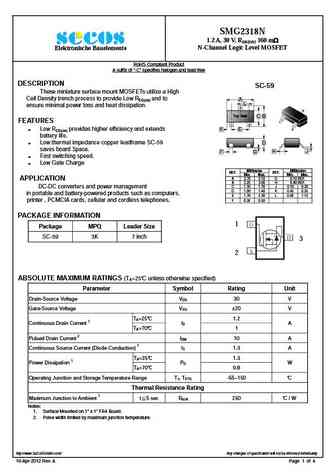
SMG2318N 1.2 A, 30 V, RDS(ON) 160 m N-Channel Logic Level MOSFET Elektronische Bauelemente RoHS Compliant Product A suffix of -C specifies halogen and lead-free DESCRIPTION SC-59 These miniature surface mount MOSFETs utilize a High Cell Density trench process to provide Low RDS(on) and to A L ensure minimal power loss and heat dissipation. 3 3 T
smg2390n.pdf
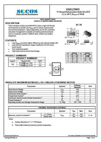
SMG2390N N-Channel Enhancement Mode Mos.FET 1.1 A, 150 V, RDS(ON) 0.700 Elektronische Bauelemente RoHS Compliant Product A suffix of -C specifies halogen and lead-free DESCRIPTION SC-59 These miniature surface mount MOSFETs utilize a High Cell Density trench process to provide Low RDS(on) and to ensure minimal power A L loss and heat dissipation. Typical applica
smg2330n.pdf
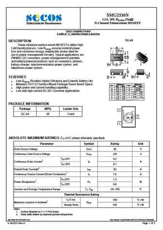
SMG2330N 5.2A, 30V, RDS(ON) 32m N-Channel Enhancement MOSFET Elektronische Bauelemente RoHS Compliant Product A suffix of -C specifies halogen & lead-free SC-59 DESCRIPTION These miniature surface mount MOSFETs utilize High A Cell Density process. Low RDS(on) assures minimal power L loss and conserves energy, making this device ideal for 3 3 use
smg2310a.pdf
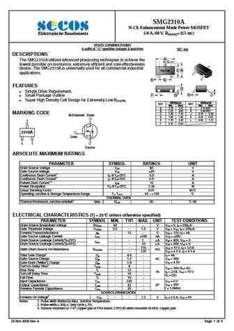
SMG2310A N-Ch Enhancement Mode Power MOSFET 5.0 A, 60 V, RDS(ON)=115 m Elektronische Bauelemente sRoHS Compliant Product A suffix of -C specifies halogen & lead-free SC-59 DESCRIPTIONS A The SMG2310A utilized advanced processing techniques to achieve the L lowest possible on-resistance, extremely efficient and cost-effectiveness 3 3 device. The SMG2310A is univers
smg2305p.pdf
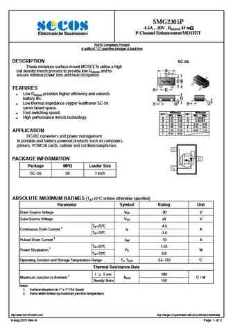
SMG2305P -4.5A , -20V , RDS(ON) 43 m P-Channel Enhancement MOSFET Elektronische Bauelemente RoHS Compliant Product A suffix of -C specifies halogen & lead-free DESCRIPTION SC-59 These miniature surface mount MOSFETs utilize a high A cell density trench process to provide low RDS(on) and to L ensure minimal power loss and heat dissipation. 3 3 Top
smg2325p.pdf
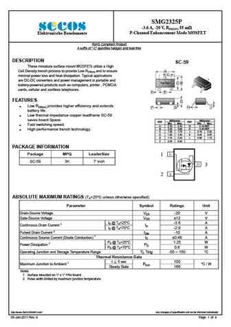
SMG2325P -3.6 A, -20 V, RDS(ON) 55 m P-Channel Enhancement Mode MOSFET Elektronische Bauelemente RoHS Compliant Product A suffix of -C specifies halogen and lead-free DESCRIPTION SC-59 These miniature surface mount MOSFETs utilize a High Cell Density trench process to provide Low RDS(on) and to ensure A L minimal power loss and heat dissipation. Typical applicati
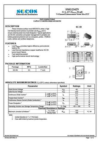
smg2342ne.pdf
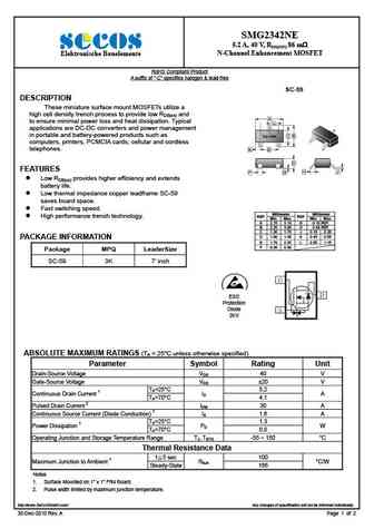
SMG2342NE 5.2 A, 40 V, RDS(ON) 86 m N-Channel Enhancement MOSFET Elektronische Bauelemente RoHS Compliant Product A suffix of -C specifies halogen & lead-free SC-59 DESCRIPTION These miniature surface mount MOSFETs utilize a high cell density trench process to provide low RDS(on) and A to ensure minimal power loss and heat dissipation. Typical L 3 applications
smg2391p.pdf
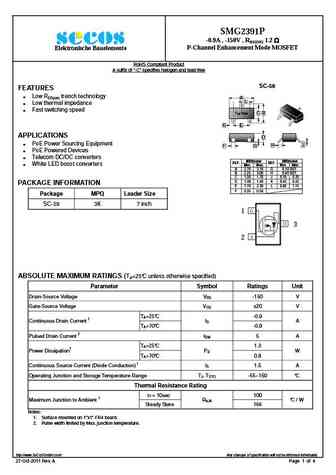
SMG2391P -0.9A , -150V , RDS(ON) 1.2 P-Channel Enhancement Mode MOSFET Elektronische Bauelemente RoHS Compliant Product A suffix of -C specifies halogen and lead-free SC-59 FEATURES Low RDS(on) trench technology A L Low thermal impedance 3 3 Fast switching speed Top View C B 1 1 2 2 K E APPLICATIONS D PoE Power Sourcing Equipment
smg2306n.pdf
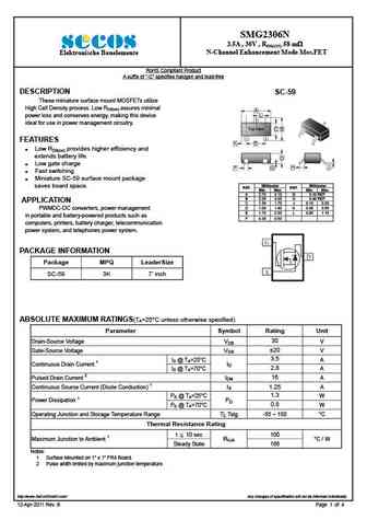
SMG2306N 3.5A , 30V , RDS(ON) 58 m N-Channel Enhancement Mode Mos.FET Elektronische Bauelemente RoHS Compliant Product A suffix of -C specifies halogen and lead-free DESCRIPTION SC-59 These miniature surface mount MOSFETs utilize High Cell Density process. Low RDS(on) assures minimal A L power loss and conserves energy, making this device 3 3 ideal for use in
smg2306a.pdf
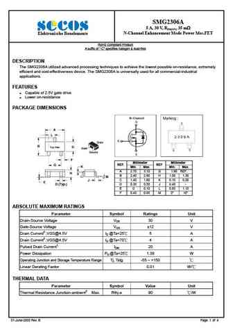
SMG2306A 5 A, 30 V, RDS(ON) 35 m N-Channel Enhancement Mode Power Mos.FET Elektronische Bauelemente RoHS Compliant Product A suffix of -C specifies halogen & lead-free DESCRIPTION The SMG2306A utilized advanced processing techniques to achieve the lowest possible on-resistance, extremely efficient and cost-effectiveness device. The SMG2306A is universally used for all co
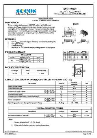
smg2398ne.pdf
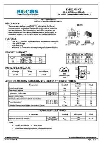
SMG2398NE 2.2 A, 60 V, RDS(ON) 194 m N-Channel Enhancement Mode Mos.FET Elektronische Bauelemente RoHS Compliant Product A suffix of -C specifies halogen and lead-free DESCRIPTION SC-59 These miniature surface mount MOSFETs utilize a High Cell Density trench process to provide Low RDS(on) and to ensure minimal power loss A L and heat dissipation. Typical applicat
smg2322n.pdf
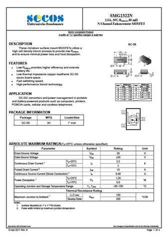
SMG2322N 2.5A, 30V, RDS(ON) 85 m N-Channel Enhancement MOSFET Elektronische Bauelemente RoHS Compliant Product A suffix of -C specifies halogen & lead-free DESCRIPTION SC-59 These miniature surface mount MOSFETs utilize a high cell density trench process to provide low RDS(on) A L and to ensure minimal power loss and heat dissipation. 3 3 Top View C B 1 1 2
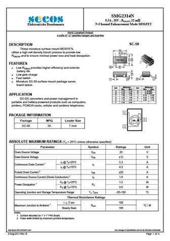
smg2314ne.pdf
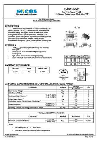
SMG2314NE 4 A, 20 V, RDS(ON) 32 m N-Channel Enhancement Mode Mos.FET Elektronische Bauelemente RoHS Compliant Product A suffix of -C specifies halogen and lead-free DESCRIPTION SC-59 These miniature surface mount MOSFETs utilize High Cell Density process. Low RDS(on) assures minimal power loss and A L conserves energy, making this device ideal for use in power
smg2336n.pdf
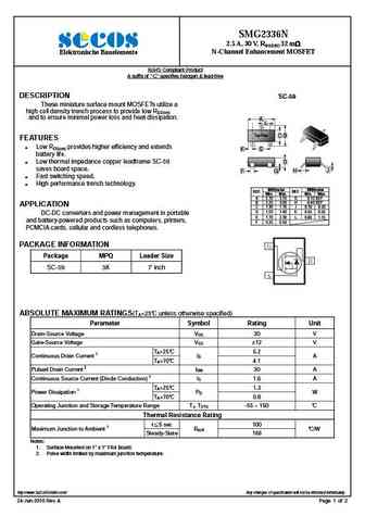
SMG2336N 2.5 A, 30 V, RDS(ON) 32 m N-Channel Enhancement MOSFET Elektronische Bauelemente RoHS Compliant Product A suffix of -C specifies halogen & lead-free DESCRIPTION SC-59 These miniature surface mount MOSFETs utilize a high cell density trench process to provide low RDS(on) and to ensure minimal power loss and heat dissipation. A L 3 3 Top
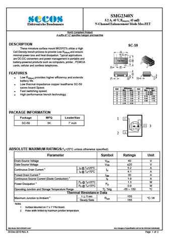
smg2340ne.pdf
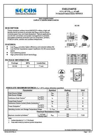
SMG2340NE 5.2 A, 40 V, RDS(ON) 43 m N-Channel Enhancement MOSFET Elektronische Bauelemente RoHS Compliant Product A suffix of -C specifies halogen & lead-free SC-59 DESCRIPTION These miniature surface mount MOSFETs utilize a high cell density trench process to provide low RDS(on) and to ensure A minimal power loss and heat dissipation. Typical applications L 3 ar
smg2310n.pdf
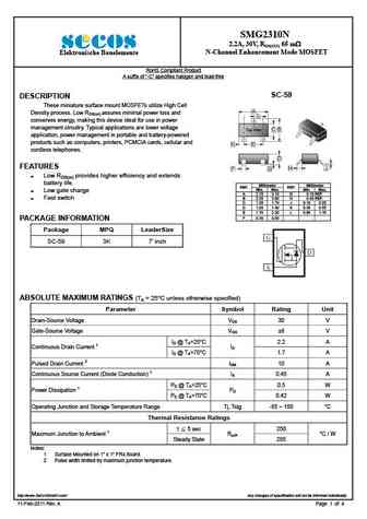
SMG2310N 2.2A, 30V, RDS(ON) 65 m N-Channel Enhancement Mode MOSFET Elektronische Bauelemente RoHS Compliant Product A suffix of -C specifies halogen and lead-free SC-59 DESCRIPTION These miniature surface mount MOSFETs utilize High Cell A Density process. Low RDS(on) assures minimal power loss and L conserves energy, making this device ideal for use in power 3 3
smg2328.pdf
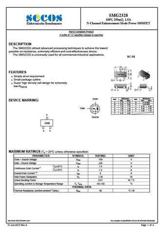
SMG2328 100V, 250m , 1.5A N-Channel Enhancement Mode Power MOSFET Elektronische Bauelemente RoHS Compliant Product A Suffix of -C specifies halogen & lead-free DESCRIPTION The SMG2328 utilized advanced processing techniques to achieve the lowest possible on-resistance, extremely efficient and cost-effectiveness device. The SMG2328 is universally used for all commercia
smg2305pe.pdf
SMG2305PE -4.5 A, -20 V, RDS(ON) 43 m P-Channel Enhancement MOSFET Elektronische Bauelemente RoHS Compliant Product A suffix of -C specifies halogen & lead-free DESCRIPTION SC-59 These miniature surface mount MOSFETs utilize a high cell density trench process to provide low RDS(on) and to A L ensure minimal power loss and heat dissipation. Typical 3 3 applicat
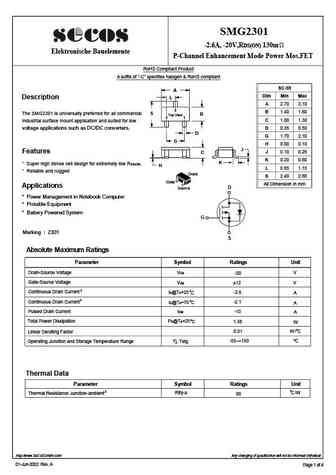
smg2301p.pdf
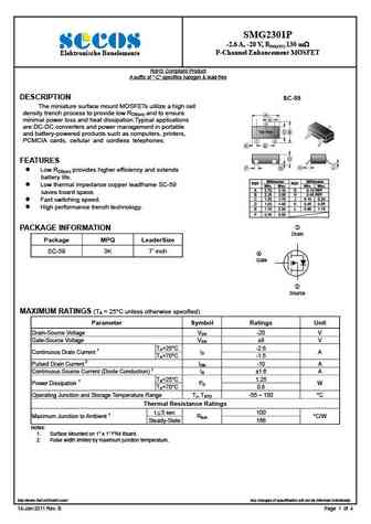
SMG2301P -2.6 A, -20 V, RDS(ON) 130 m P-Channel Enhancement MOSFET Elektronische Bauelemente RoHS Compliant Product A suffix of -C specifies halogen & lead-free DESCRIPTION SC-59 The miniature surface mount MOSFETs utilize a high cell density trench process to provide low RDS(on) and to ensure A L minimal power loss and heat dissipation.Typical applications 3 3
smg2329p.pdf
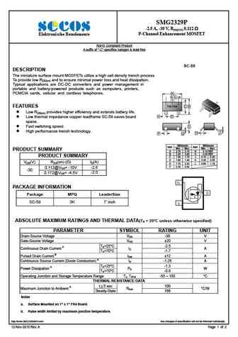
SMG2329P -2.5 A, -30 V, RDS(ON) 0.112 P-Channel Enhancement MOSFET Elektronische Bauelemente RoHS Compliant Product A suffix of -C specifies halogen & lead-free SC-59 DESCRIPTION The miniature surface mount MOSFETs utilize a high cell density trench process To provide low RDS(on) and to ensure minimal power loss and heat dissipation. Typical applications are DC-DC
smg2398n.pdf
SMG2398N 2.2 A, 60 V, RDS(ON) 194 m N-Channel Enhancement Mode Mos.FET Elektronische Bauelemente RoHS Compliant Product A suffix of -C specifies halogen and lead-free DESCRIPTION SC-59 These miniature surface mount MOSFETs utilize High Cell Density process. Low RDS(on) assures minimal power loss and conserves energy, A L making this device ideal for use in power
smg2326n.pdf
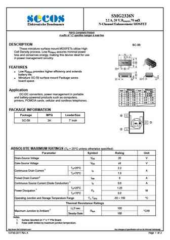
SMG2326N 2.2 A, 20 V, RDS(ON) 70 m N-Channel Enhancement MOSFET Elektronische Bauelemente RoHS Compliant Product A suffix of -C specifies halogen & lead-free DESCRIPTION SC-59 These miniature surface mount MOSFETs utilize High Cell Density process. Low RDS(on) assures minimal power loss and conserves energy, making this device ideal for use A L in power management
smg2358n.pdf
SMG2358N 2.8 A, 60 V, RDS(ON) 92 m N-Channel Enhancement Mode Mos.FET Elektronische Bauelemente RoHS Compliant Product A suffix of -C specifies halogen and lead-free DESCRIPTION SC-59 These miniature surface mount MOSFETs utilize a High Cell Density trench process to provide Low RDS(on) and to ensure minimal power A L loss and heat dissipation. Typical applicatio
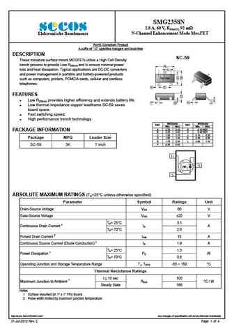
smg2328ne.pdf
SMG2328NE 6.3 A, 20 V, RDS(ON) 22 m N-Channel Enhancement MOSFET Elektronische Bauelemente RoHS Compliant Product A suffix of -C specifies halogen & lead-free SC-59 DESCRIPTION These miniature surface mount MOSFETs utilize a high cell density trench process to provide low RDS(on) and to A L ensure minimal power loss and heat dissipation. Typical 3 3 applicati
smg2319p.pdf
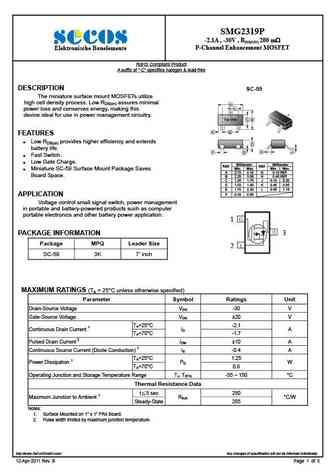
SMG2319P -2.1A , -30V , RDS(ON) 200 m P-Channel Enhancement MOSFET Elektronische Bauelemente RoHS Compliant Product A suffix of -C specifies halogen & lead-free DESCRIPTION SC-59 The miniature surface mount MOSFETs utilize high cell density process. Low RDS(on) assures minimal A L power loss and conserves energy, making this 3 3 device ideal for use in power m
smg2306ne.pdf
SMG2306NE 3.5A , 30V , RDS(ON) 58 m N-Channel Enhancement Mode Mos.FET Elektronische Bauelemente RoHS Compliant Product A suffix of -C specifies halogen and lead-free SC-59 DESCRIPTION These miniature surface mount MOSFETs utilize A L High Cell Density process. Low RDS(on) assures 3 3 minimal power loss and conserves energy, making Top View C B this device i
smg2334ne.pdf
SMG2334NE 3.5A , 30V , RDS(ON) 58 m N-Channel Enhancement MOSFET Elektronische Bauelemente RoHS Compliant Product A suffix of -C specifies halogen & lead-free SC-59 DESCRIPTION These miniature surface mount MOSFETs utilize a high A cell density trench process to provide low RDS(on) and to L ensure minimal power loss and heat dissipation. 3 3 Top View C B 1 1
smg2301.pdf
SMG2301 -2.6A, -20V,RDS(ON) 130m Elektronische Bauelemente P-Channel Enhancement Mode Power Mos.FET RoHS Compliant Product A suffix of "-C" specifies halogen & RoHS compliant SC-59 A Dim Min Max Description L A 2.70 3.10 3 B 1.40 1.60 The SMG2301 is universally preferred for all commercial S B Top View 2 1 C 1.00 1.30 industrial surface mount application and suited for l
smg2343.pdf
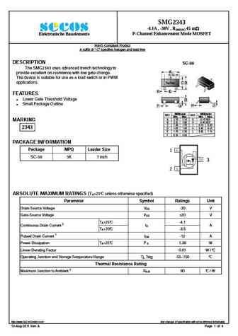
SMG2343 -4.1A , -30V , RDS(ON) 45 m P-Channel Enhancement Mode MOSFET Elektronische Bauelemente RoHS Compliant Product A suffix of -C specifies halogen and lead-free DESCRIPTION SC-59 The SMG2343 uses advanced trench technology to A provide excellent on-resistance with low gate change. L 3 The device is suitable for use as a load switch or in PW
smg2342n.pdf
SMG2342N 5.2 A, 40 V, RDS(ON) 86 m N-Channel Enhancement Mode Mos.FET Elektronische Bauelemente RoHS Compliant Product A suffix of -C specifies halogen and lead-free DESCRIPTION SC-59 These miniature surface mount MOSFETs utilize a High Cell Density trench process to provide Low RDS(on) and to A L ensure minimal power loss heat dissipation. Typical applications
smg2359p.pdf
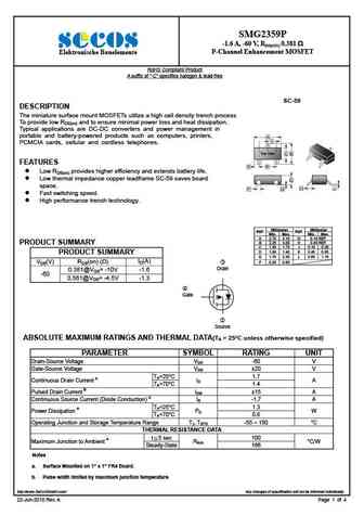
SMG2359P -1.6 A, -60 V, RDS(ON) 0.381 P-Channel Enhancement MOSFET Elektronische Bauelemente RoHS Compliant Product A suffix of -C specifies halogen & lead-free SC-59 DESCRIPTION The miniature surface mount MOSFETs utilize a high cell density trench process To provide low RDS(on) and to ensure minimal power loss and heat dissipation. Typical applications are DC-DC
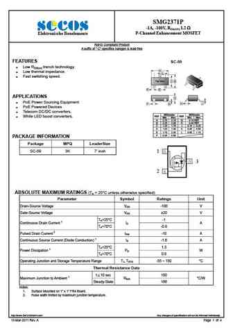
smg2339p.pdf
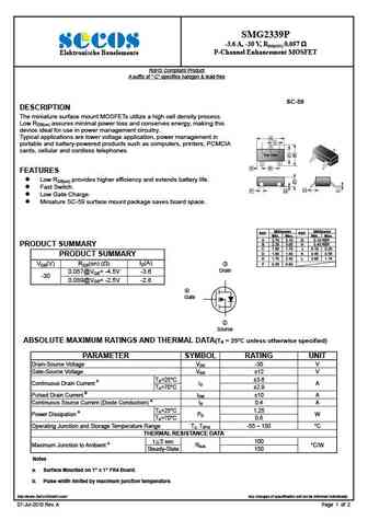
SMG2339P -3.6 A, -30 V, RDS(ON) 0.057 P-Channel Enhancement MOSFET Elektronische Bauelemente RoHS Compliant Product A suffix of -C specifies halogen & lead-free SC-59 DESCRIPTION The miniature surface mount MOSFETs utilize a high cell density process Low RDS(on) assures minimal power loss and conserves energy, making this device ideal for use in power management ci
smg2302n.pdf
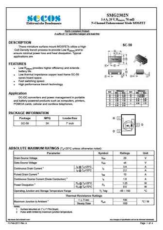
SMG2302N 3.4 A, 20 V, RDS(ON) 76 m N-Channel Enhancement Mode MOSFET Elektronische Bauelemente RoHS Compliant Product A suffix of -C specifies halogen and lead-free DESCRIPTION SC-59 These miniature surface mount MOSFETs utilize a High Cell Density trench process to provide Low RDS(on) and to A L ensure minimal power loss and heat dissipation. Typical 3 3 app
smg2314n.pdf
SMG2314N 5.3A , 20V , RDS(ON) 32 m N-Channel Enhancement Mode MOSFET Elektronische Bauelemente RoHS Compliant Product A suffix of -C specifies halogen and lead-free SC-59 DESCRIPTION These miniature surface mount MOSFETs A utilize a high cell density trench process to provide low L 3 RDS(ON) and to ensure minimal power loss and heat dissipation. 3 Top View C
smg2370n.pdf
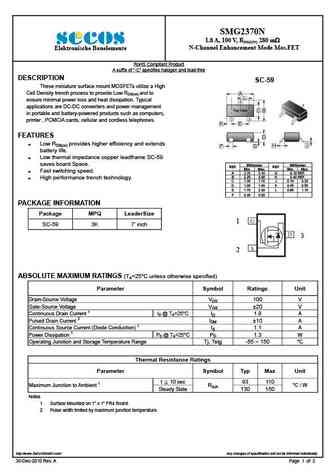
SMG2370N 1.8 A, 100 V, RDS(ON) 280 m N-Channel Enhancement Mode Mos.FET Elektronische Bauelemente RoHS Compliant Product A suffix of -C specifies halogen and lead-free DESCRIPTION SC-59 These miniature surface mount MOSFETs utilize a High Cell Density trench process to provide Low RDS(on) and to A L ensure minimal power loss and heat dissipation. Typical 3 3
smg2340n.pdf
SMG2340N 5.2 A, 40 V, RDS(ON) 43 m N-Channel Enhancement Mode Mos.FET Elektronische Bauelemente RoHS Compliant Product A suffix of -C specifies halogen and lead-free DESCRIPTION SC-59 These miniature surface mount MOSFETs utilize a High Cell Density trench process to provide Low RDS(on) and ensure A L minimal power loss and heat dissipation. Typical applications
smg2328s.pdf
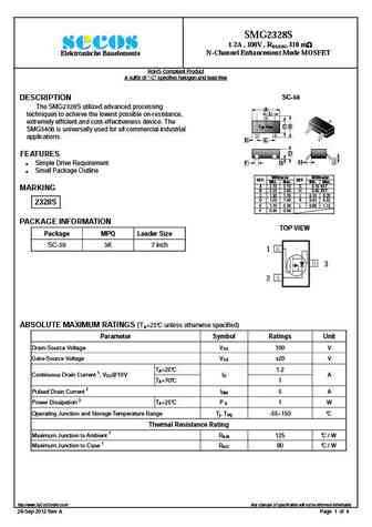
SMG2328S 1.2A , 100V , RDS(ON) 310 m N-Channel Enhancement Mode MOSFET Elektronische Bauelemente RoHS Compliant Product A suffix of -C specifies halogen and lead-free SC-59 DESCRIPTION The SMG2328S utilized advanced processing A L techniques to achieve the lowest possible on-resistance, 3 3 extremely efficient and cost-effectiveness device. The
g2302.pdf
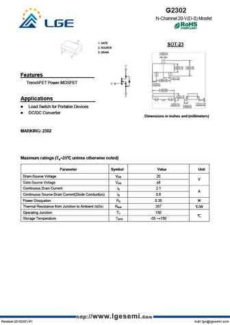
G2302 N-Channel 20-V(D-S) Mosfet 1. GATE SOT-23 2. SOURCE 3. DRAIN Features TrenchFET Power MOSFET Applications Load Switch for Portable Devices DC/DC Converter Dimensions in inches and (millimeters) MARKING 2302 Maximum ratings (Ta=25 unless otherwise noted) Parameter Symbol Value Unit Drain-Source Voltage VDS 20 V Gate-Source Voltage VGS 8 Continuous Dra
g2305.pdf
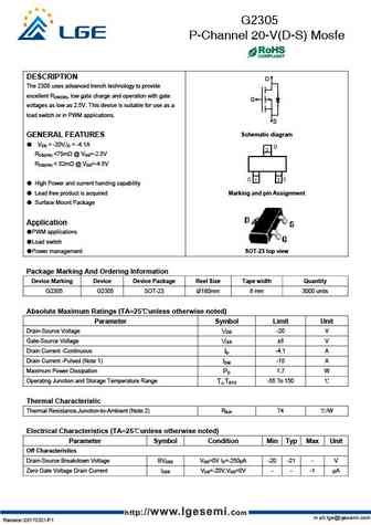
G2305 P-Channel 20-V(D-S) Mosfe DESCRIPTION D The 2305 uses advanced trench technology to provide excellent RDS(ON), low gate charge and operation with gate G voltages as low as 2.5V. This device is suitable for use as a load switch or in PWM applications. S Schematic diagram GENERAL FEATURES VDS = -20V,ID = -4.1A RDS(ON)
smg2305l.pdf
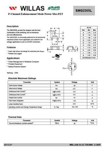
FM120-M WILLAS SMG2305L THRU P-Channel Enhancement Mode Power Mos.FET FM1200-M 1.0A SURFACE MOUNT SCHOTTKY BARRIER RECTIFIERS -20V- 200V SOD-123 PACKAGE Pb Free Product Package outline Features Batch process design, excellent power dissipation offers better r Descriptioneverse leakage current and thermal resistance. SOD-123H SC-59 Low profile surface mounted applic
g2304.pdf
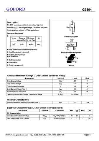
GOFORD G2304 D Description The 2304 uses advanced trench technology to provide G excellent RDS(ON) and low gate charge .This device is suitable for use as a load switch or in PWM applications. General Features S Schematic diagram VDSS RDS(ON) RDS(ON) ID @ 4.5V (Typ) @ 10V (Typ) m m 3.6 30V 61 47 A G2304 High power and current handing capability Lead f
g2305.pdf
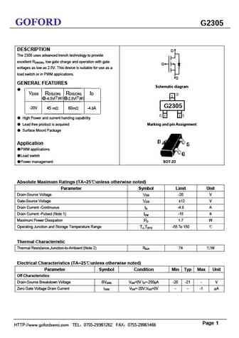
GOFORD G2305 DESCRIPTION D The 2305 uses advanced trench technology to provide excellent RDS(ON), low gate charge and operation with gate G voltages as low as 2.5V. This device is suitable for use as a load switch or in PWM applications. S GENERAL FEATURES Schematic diagram VDSS RDS(ON) RDS(ON) ID (Typ) @-2.5V @-4.5V (Typ) G2305 -20V 45 m 60m -4.8 A
3cg23.pdf
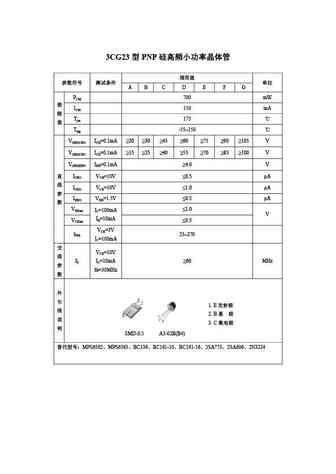
3CG23 PNP A B C D E F G PCM 700 mW ICM 150 mA Tjm 175 Tstg -55 150 V(BR)CBO ICB=0.1mA 20 30 45 60 75 90 105 V V(BR)CEO ICE=0.1mA 15 25 40 55 70 85 100 V V(BR)EBO IEB=0.1mA 4.0 V ICBO VCB=10V 0.5 A ICEO VCE=10V 1.
dmg2301u.pdf
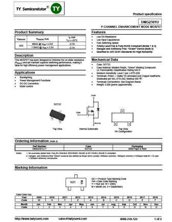
Product specification DMG2301U P-CHANNEL ENHANCEMENT MODE MOSFET Product Summary Features Low On-Resistance ID max V(BR)DSS RDS(ON) max Low Input Capacitance TA = +25 C Fast Switching Speed 80m @ VGS = 4.5V -2.7A -20V Totally Lead-Free & Fully RoHS Compliant (Notes 1 & 2) 110m @ VGS = 2.5V -2.1A Halogen and Antimony Free. Green Device (N
dmg2307l.pdf
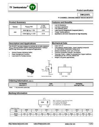
Product specification DMG2307L P-CHANNEL ENHANCEMENT MODE MOSFET Product Summary Features and Benefits Low On-Resistance ID max V(BR)DSS RDS(ON) max Low Input Capacitance TA = 25 C Fast Switching Speed 90m @ VGS = -10V -3.8A Lead Free By Design/RoHS Compliant (Note 1) "Green" Device (Note 2) -30V 134m @ VGS = -4.5V -3.1A Qualified to AEC-Q10
dmg2302u.pdf
Product specification DMG2302U N-CHANNEL ENHANCEMENT MODE MOSFET Features Mechanical Data Low On-Resistance Case SOT-23 Low Input Capacitance Case Material Molded Plastic, Green Molding Compound. UL Flammability Classification Rating 94V-0 Fast Switching Speed Moisture Sensitivity Level 1 per J-STD-020D Low Input/Output Leakage Terminal
3dg2308.pdf
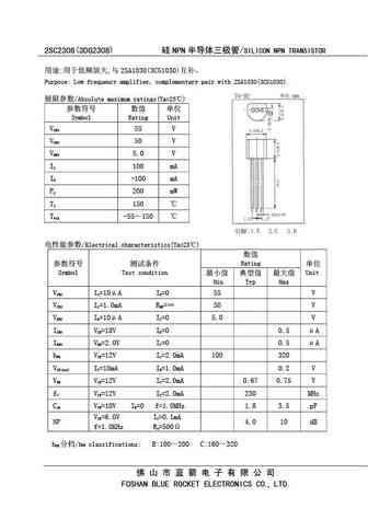
2SC2308(3DG2308) NPN /SILICON NPN TRANSISTOR , 2SA1030(3CG1030) Purpose Low frequency amplifier, complementary pair with 2SA1030(3CG1030). /Absolute maximum ratings(Ta=25 ) Symbol Rating Unit V 55 V CBO V 50 V CEO V 5.0 V EBO I 100 mA C I -100 mA E P 200 mW C T
3dg2383.pdf
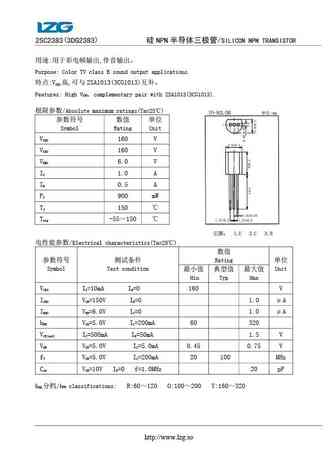
2SC2383(3DG2383) NPN /SILICON NPN TRANSISTOR , Purpose Color TV class B sound output applications. V , 2SA1013(3CG1013) CEO Features High V , complementary pair with 2SA1013(3CG1013). CEO /Absolute maximum ratings(Ta=25 ) Symbol Rating Unit V 160
3dg2383t.pdf
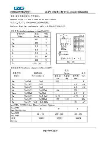
2SC2383T(3DG2383T) NPN /SILICON NPN TRANSISTOR , Purpose Color TV class B sound output applications. V , 2SA1013T(3CG1013T) CEO Features High V , complementary pair with 2SA1013T(3CG1013T). CEO /Absolute maximum ratings(Ta=25 ) Symbol Rating Unit
sg23n06t.pdf
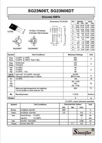
SG23N06T, SG23N06DT Discrete IGBTs Dimensions TO-247AD Dim. Millimeter Inches Min. Max. Min. Max. A 19.81 20.32 0.780 0.800 B 20.80 21.46 0.819 0.845 C 15.75 16.26 0.610 0.640 E G=Gate, C=Collector, D 3.55 3.65 0.140 0.144 C(TAB) C E=Emitter,TAB=Collector G E 4.32 5.49 0.170 0.216 F 5.4 6.2 0.212 0.244 G 1.65 2.13 0.065 0.084 H - 4.5 - 0.177 J 1.0 1.4 0.040 0.055 K 10.8 11.0
sg23n06dt.pdf

SG23N06T, SG23N06DT Discrete IGBTs Dimensions TO-247AD Dim. Millimeter Inches Min. Max. Min. Max. A 19.81 20.32 0.780 0.800 B 20.80 21.46 0.819 0.845 C 15.75 16.26 0.610 0.640 E G=Gate, C=Collector, D 3.55 3.65 0.140 0.144 C(TAB) C E=Emitter,TAB=Collector G E 4.32 5.49 0.170 0.216 F 5.4 6.2 0.212 0.244 G 1.65 2.13 0.065 0.084 H - 4.5 - 0.177 J 1.0 1.4 0.040 0.055 K 10.8 11.0
dmg2301u.pdf
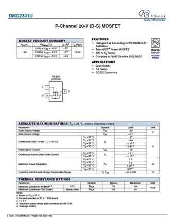
DMG2301U www.VBsemi.tw P-Channel 20-V (D-S) MOSFET FEATURES MOSFET PRODUCT SUMMARY Halogen-free According to IEC 61249-2-21 VDS (V) RDS(on) ( )ID (A)a Qg (Typ.) Definition 0.035 at VGS = - 10 V - 5e TrenchFET Power MOSFET e - 20 0.043 at VGS = - 4.5 V - 5 10 nC 100 % Rg Tested 0.061 at VGS = - 2.5 V - 4.8 Compliant to RoHS Directive 2002/95/EC APPLICATION
dmg2307l.pdf

DMG2307L www.VBsemi.tw P-Channel 30 V (D-S) MOSFET FEATURES PRODUCT SUMMARY TrenchFET Power MOSFET 100 % Rg Tested VDS (V) RDS(on) ( ) Typ. ID (A)a Qg (Typ.) 0.046 at VGS = - 10 V - 5.6 0.049 at VGS = - 6 V - 5 11.4 nC - 30 APPLICATIONS 0.054 at VGS = - 4.5 V -4.5 For Mobile Computing - Load Switch - Notebook Adaptor Switch S TO-236 - DC/DC Converter (SOT-23
g2309.pdf
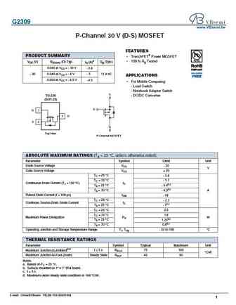
G2309 www.VBsemi.tw P-Channel 30 V (D-S) MOSFET FEATURES PRODUCT SUMMARY TrenchFET Power MOSFET 100 % Rg Tested VDS (V) RDS(on) ( ) Typ. ID (A)a Qg (Typ.) 0.046 at VGS = - 10 V - 5.6 0.049 at VGS = - 6 V - 5 11.4 nC - 30 APPLICATIONS 0.054 at VGS = - 4.5 V -4.5 For Mobile Computing - Load Switch - Notebook Adaptor Switch S TO-236 - DC/DC Converter (SOT-23)
smg2339p.pdf
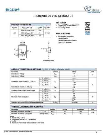
SMG2339P www.VBsemi.tw P-Channel 30 V (D-S) MOSFET FEATURES PRODUCT SUMMARY TrenchFET Power MOSFET 100 % Rg Tested VDS (V) RDS(on) ( ) Typ. ID (A)a Qg (Typ.) 0.046 at VGS = - 10 V - 5.6 0.049 at VGS = - 6 V - 5 11.4 nC - 30 APPLICATIONS 0.054 at VGS = - 4.5 V -4.5 For Mobile Computing - Load Switch - Notebook Adaptor Switch S TO-236 - DC/DC Converter (SOT-23
g2306a.pdf
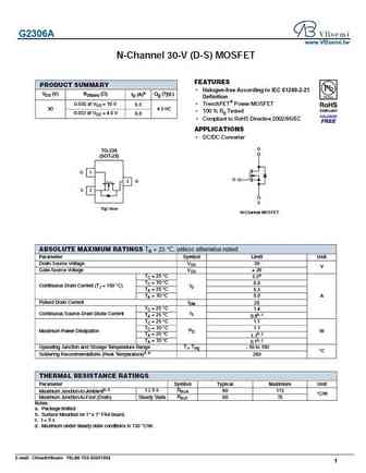
G2306A www.VBsemi.tw N-Channel 30-V (D-S) MOSFET FEATURES PRODUCT SUMMARY Halogen-free According to IEC 61249-2-21 VDS (V) RDS(on) ( ) ID (A)a Qg (Typ.) Definition 0.030 at VGS = 10 V TrenchFET Power MOSFET 6.5 30 4.5 nC 100 % Rg Tested 0.033 at VGS = 4.5 V 6.0 Compliant to RoHS Directive 2002/95/EC APPLICATIONS DC/DC Converter D TO-236 (SOT-23) G 1
Другие MOSFET... G66 , G66-3L , G68 , G69 , G80N06 , G96 , GD1 , G22 , 10N60 , G11 , G16 , G17 , 03N06 , 05N06 , 100N03 , 100P03 , 10N03 .
History: IRFP1405 | IRFP260M | IRFP4321 | IRFP4310Z | IRFIB41N15D | IRFL014N | IRFI4410Z
History: IRFP1405 | IRFP260M | IRFP4321 | IRFP4310Z | IRFIB41N15D | IRFL014N | IRFI4410Z
🌐 : EN ES РУ

Список транзисторов
Обновления
MOSFET: ASB80R750E | ASB70R380E | ASB65R300E | ASB65R220E | ASB65R120EFD | ASB60R150E | ASA80R900E | ASA80R750E | ASA80R290E | ASA70R950E | ASA70R600E | ASA70R380E | ASA70R240E | ASA65R850E | ASA65R550E | ASA65R350E
Popular searches
2sb549 | 5n50 mosfet equivalent | a1016 transistor | a1693 transistor | a933 datasheet | c535 transistor | irf3205 reemplazo | mpsu06