630A. Аналоги и основные параметры
Наименование производителя: 630A
Тип транзистора: MOSFET
Полярность: N
Предельные значения
Pd ⓘ
- Максимальная рассеиваемая мощность: 83 W
|Vds|ⓘ - Максимально допустимое напряжение сток-исток: 200 V
|Vgs|ⓘ - Максимально допустимое напряжение затвор-исток: 30 V
|Id| ⓘ - Максимально допустимый постоянный ток стока: 9 A
Tj ⓘ - Максимальная температура канала: 150 °C
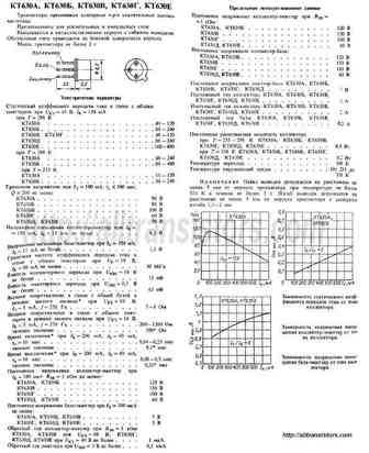
Электрические характеристики
tr ⓘ -
Время нарастания: 10.7 ns
Cossⓘ - Выходная емкость: 51.5 pf
RDSonⓘ - Сопротивление сток-исток открытого транзистора: 0.25 Ohm
Тип корпуса: TO251
TO252
- подборⓘ MOSFET транзистора по параметрам
630A даташит
..1. Size:1953K goford
630a.pdf 
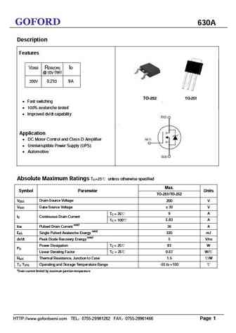
GOFORD 630A Description Features VDSS RDS(ON) ID @ 10V (typ) 9A 200V 0.21 TO-252 TO-251 Fast switching 100% avalanche tested Improved dv/dt capability Application DC Motor Control and Class D Amplifier Uninterruptible Power Supply (UPS) Automotive Absolute Maximum Ratings TC=25 unless otherwise specified Max. Symbol Parameter Unit
0.2. Size:68K fairchild semi
fdd6630a.pdf 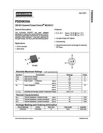
April 2001 FDD6630A 30V N-Channel PowerTrench MOSFET General Description Features This N-Channel MOSFET has been designed 21 A, 30 V R = 35 m @ V = 10 V DS(ON) GS specifically to improve the overall efficiency of DC/DC R = 50 m @ V = 4.5 V DS(ON) GS converters using either synchronous or conventional switching PWM controllers. It has been optimized for Low g
0.3. Size:69K fairchild semi
fds6630a.pdf 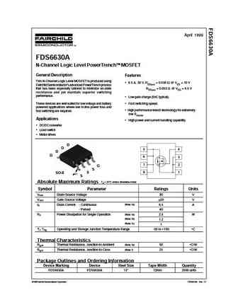
April 1999 FDS6630A N-Channel Logic Level PowerTrenchTM MOSFET General Description Features This N-Channel Logic Level MOSFET is produced using 6.5 A, 30 V. RDS(on) = 0.038 @ VGS = 10 V Fairchild Semiconductor's advanced PowerTrench process that has been especially tailored to minimize on-state RDS(on) = 0.053 @ VGS = 4.5 V resistance and yet maintain superior switching pe
0.4. Size:226K fairchild semi
irlw630a irli630a.pdf 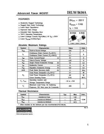
IRLW/I630A FEATURES BVDSS = 200 V Avalanche Rugged Technology RDS(on) = 0.4 Rugged Gate Oxide Technology Lower Input Capacitance ID = 9 A Improved Gate Charge Extended Safe Operating Area D2-PAK I2-PAK 150 C Operating Temperature 2 Lower Leakage Current 10 A (Max.) @ VDS = 200V Lower RDS(ON) 0.335 (Typ.) 1 1 2 3 3 1. Gate 2. Drain 3
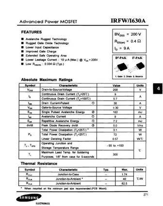
0.5. Size:509K samsung
irfw630a.pdf 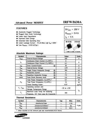
Advanced Power MOSFET FEATURES BVDSS = 200 V Avalanche Rugged Technology RDS(on) = 0.4 Rugged Gate Oxide Technology Lower Input Capacitance ID = 9 A Improved Gate Charge Extended Safe Operating Area Lower Leakage Current 10 A (Max.) @ VDS = 200V 2 Low RDS(ON) 0.333 (Typ.) 1 1 2 3 3 1. Gate 2. Drain 3. Source Absolute Maximum Ratings Symbol Charact
0.6. Size:508K samsung
irfs630a.pdf 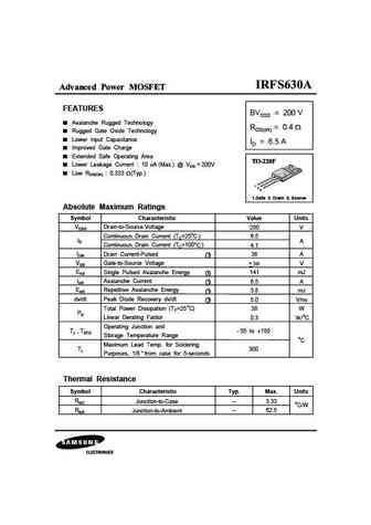
Advanced Power MOSFET FEATURES BVDSS = 200 V Avalanche Rugged Technology RDS(on) = 0.4 Rugged Gate Oxide Technology Lower Input Capacitance ID = 6.5 A Improved Gate Charge Extended Safe Operating Area Lower Leakage Current 10 A (Max.) @ VDS = 200V Low RDS(ON) 0.333 (Typ.) 1 2 3 1.Gate 2. Drain 3. Source Absolute Maximum Ratings Symbol Characteristic Valu
0.7. Size:911K samsung
irl630a.pdf 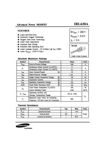
Advanced Power MOSFET FEATURES BVDSS = 200 V Logic-Level Gate Drive RDS(on) = 0.4 Avalanche Rugged Technology Rugged Gate Oxide Technology ID = 9 A Lower Input Capacitance Improved Gate Charge Extended Safe Operating Area Lower Leakage Current 10 A (Max.) @ VDS = 200V Lower RDS(ON) 0.335 (Typ.) 1 2 3 1.Gate 2. Drain 3. Source Absolute Maximum Ratings
0.8. Size:945K samsung
irf630a.pdf 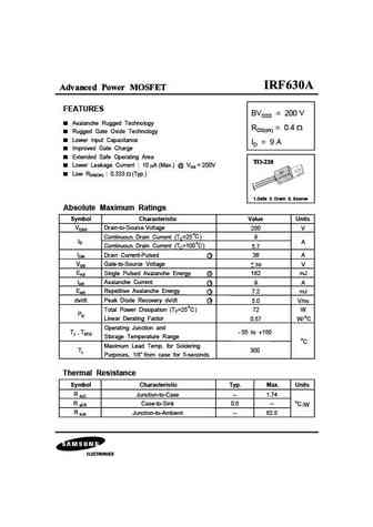
Advanced Power MOSFET FEATURES BVDSS = 200 V Avalanche Rugged Technology RDS(on) = 0.4 Rugged Gate Oxide Technology Lower Input Capacitance ID = 9 A Improved Gate Charge Extended Safe Operating Area Lower Leakage Current 10 A (Max.) @ VDS = 200V Low RDS(ON) 0.333 (Typ.) 1 2 3 1.Gate 2. Drain 3. Source Absolute Maximum Ratings Symbol Characteristic Value
0.9. Size:920K samsung
irls630a.pdf 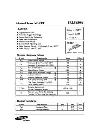
Advanced Power MOSFET FEATURES BVDSS = 200 V Logic Level Gate Drive RDS(on) = 0.4 Avalanche Rugged Technology Rugged Gate Oxide Technology ID = 6.5 A Lower Input Capacitance Improved Gate Charge Extended Safe Operating Area Lower Leakage Current 10 A (Max.) @ VDS = 200V Lower RDS(ON) 0.335 (Typ.) 1 2 3 1.Gate 2. Drain 3. Source Absolute Maximum Ratin
0.10. Size:1006K samsung
irlw630a.pdf 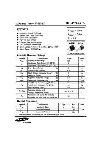
Advanced Power MOSFET FEATURES BVDSS = 200 V Avalanche Rugged Technology RDS(on) = 0.4 Rugged Gate Oxide Technology Lower Input Capacitance ID = 9 A Improved Gate Charge Extended Safe Operating Area 175 Operating Temperature 2 Lower Leakage Current 10 A (Max.) @ VDS = 200V Lower RDS(ON) 0.335 (Typ.) 1 1 2 3 3 1. Gate 2. Drain 3. Source Absolute M
0.11. Size:351K onsemi
fdd6630a.pdf 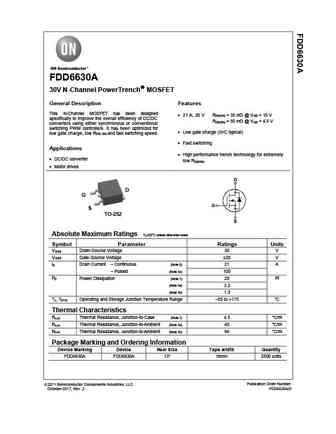
FDD6630A 30V N-Channel PowerTrench MOSFET General Description Features This N-Channel MOSFET has been designed 21 A, 30 V R = 35 m @ V = 10 V DS(ON) GS specifically to improve the overall efficiency of DC/DC R = 50 m @ V = 4.5 V DS(ON) GS converters using either synchronous or conventional switching PWM controllers. It has been optimized for Low gate charge (5n
0.13. Size:1084K feihonltd
fhu630a fhd630a fhp630a fhf630a.pdf 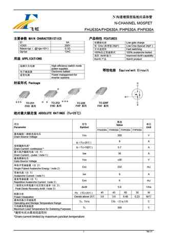
N N-CHANNEL MOSFET FHU630A/FHD630A /FHP630A /FHF630A MAIN CHARACTERISTICS FEATURES ID 9A Low gate charge VDSS 200V Crss ( 24pF) Low Crss (typical 24pF ) Rdson-typ @Vgs=10V 0.3 Fast switching Qg-typ 12nC 100% 100% avalanche tested dv/d
0.14. Size:581K samwin
swp630a1.pdf 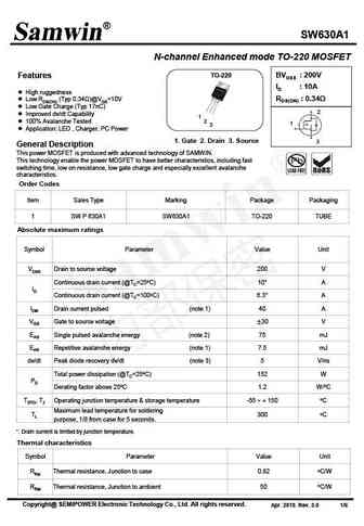
SW630A1 N-channel Enhanced mode TO-220 MOSFET TO-220 BVDSS 200V Features ID 10A High ruggedness RDS(ON) 0.34 Low RDS(ON) (Typ 0.34 )@VGS=10V Low Gate Charge (Typ 17nC) 2 Improved dv/dt Capability 1 100% Avalanche Tested 2 1 3 Application LED , Charger, PC Power 1. Gate 2. Drain 3. Source 3 General Description This power
0.15. Size:726K wuxi china
cs630a3h.pdf 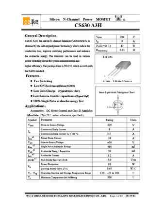
Silicon N-Channel Power MOSFET R CS630 A3H General Description VDSS 200 V CS630 A3H, the silicon N-channel Enhanced VDMOSFETs, is ID 9 A PD(TC=25 ) 83 W obtained by the self-aligned planar Technology which reduce the RDS(ON)Typ 0.23 conduction loss, improve switching performance and enhance the avalanche energy. The transistor can be used in various power swi
0.16. Size:723K wuxi china
cs630a4h.pdf 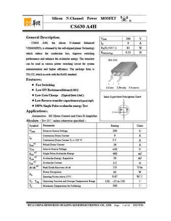
Silicon N-Channel Power MOSFET R CS630 A4H General Description VDSS 200 V CS630 A4H, the silicon N-channel Enhanced ID 9 A PD(TC=25 ) 83 W VDMOSFETs, is obtained by the self-aligned planar Technology RDS(ON)Typ 0.23 which reduce the conduction loss, improve switching performance and enhance the avalanche energy. The transistor can be used in various power swi
0.17. Size:715K wuxi china
cs630a8h.pdf 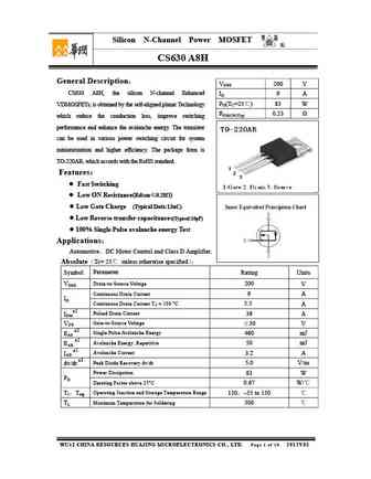
Silicon N-Channel Power MOSFET R CS630 A8H General Description VDSS 200 V CS630 A8H, the silicon N-channel Enhanced ID 9 A PD(TC=25 ) 83 W VDMOSFETs, is obtained by the self-aligned planar Technology RDS(ON)Typ 0.23 which reduce the conduction loss, improve switching performance and enhance the avalanche energy. The transistor can be used in various power sw
0.18. Size:383K jiejie micro
jmsl0630ag.pdf 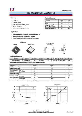
JMSL0630AG 60V 22m N-Ch Power MOSFET Features Product Summary Parameter Value Unit Low RDS(ON) VDS 60 V Low Gate Charge VGS(th) 1.7 V 100% UIS Tested, 100% Rg Tested ID (@ VGS = 10V) (1) 25 A RDS(ON) (@ VGS = 10V) Pb-free Lead Plating 22 m RDS(ON) (@ VGS = 4.5V) 28 m Halogen-free and RoHS-compliant Applications Power Managerment in Telecom.,
0.19. Size:378K jiejie micro
jmsl0630au.pdf 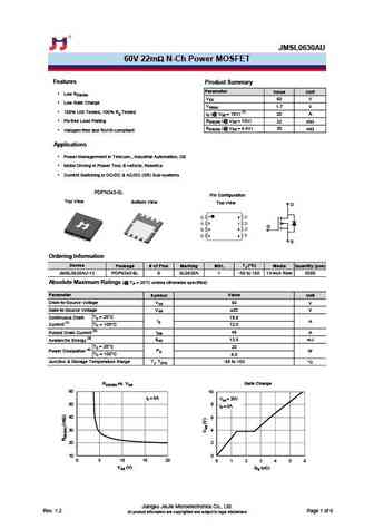
JMSL0630AU 60V 22m N-Ch Power MOSFET Features Product Summary Parameter Value Unit Low RDS(ON) VDS 60 V Low Gate Charge VGS(th) 1.7 V 100% UIS Tested, 100% Rg Tested ID (@ VGS = 10V) (1) 20 A RDS(ON) (@ VGS = 10V) Pb-free Lead Plating 22 m RDS(ON) (@ VGS = 4.5V) 30 m Halogen-free and RoHS-compliant Applications Power Managerment in Telecom.,
0.20. Size:386K jiejie micro
jmsl0630agd.pdf 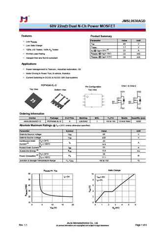
JMSL0630AGD 60V 22m Dual N-Ch Power MOSFET Features Product Summary Parameter Value Unit Low RDS(ON) VDS 60 V Low Gate Charge VGS(th) 1.7 V 100% UIS Tested, 100% Rg Tested ID (@ VGS = 10V) (1) 23 A RDS(ON) (@ VGS = 10V) Pb-free Lead Plating 22 m RDS(ON) (@ VGS = 4.5V) 28 m Halogen-free and RoHS-compliant Applications Power Managerment in
0.21. Size:1469K cn vbsemi
fds6630a.pdf 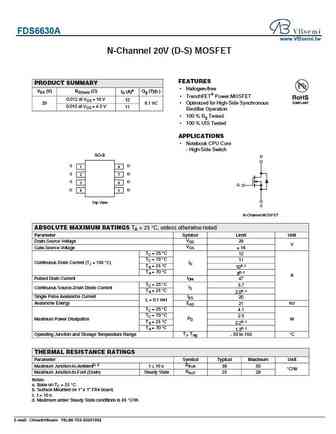
FDS6630A www.VBsemi.tw N-Channel 20V (D-S) MOSFET FEATURES PRODUCT SUMMARY Halogen-free VDS (V) RDS(on) ( ) ID (A)a Qg (Typ.) TrenchFET Power MOSFET 0.012 at VGS = 10 V 12 20 6.1 nC Optimized for High-Side Synchronous 0.015 at VGS = 4.5 V 11 Rectifier Operation 100 % Rg Tested 100 % UIS Tested APPLICATIONS Notebook CPU Core - High-Side Switch SO
0.22. Size:245K inchange semiconductor
irf630a.pdf 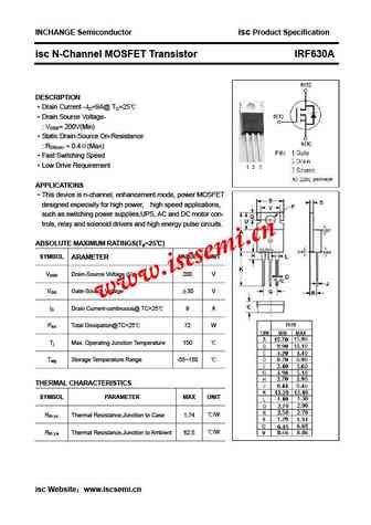
INCHANGE Semiconductor isc Product Specification isc N-Channel MOSFET Transistor IRF630A DESCRIPTION Drain Current ID=9A@ TC=25 Drain Source Voltage- VDSS= 200V(Min) Static Drain-Source On-Resistance RDS(on) = 0.4 (Max) Fast Switching Speed Low Drive Requirement APPLICATIONS This device is n-channel, enhancement mode, power MOSFET designed espec
Другие MOSFET... 80N04
, 80N08TR
, 8205A
, 8205B
, G3205
, G1010
, G3710
, 5N20A
, IRFZ44N
, 640
, 18N20
, 18N20A
, 2N25
, 3N25
, 740
, 840
, 16N50F
.