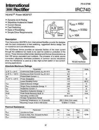
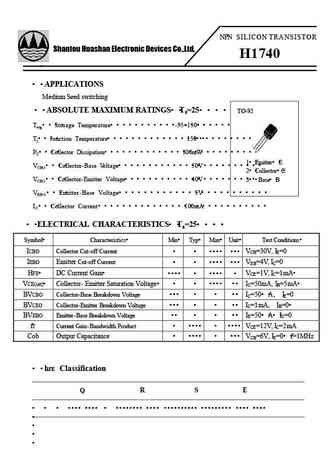
740. Аналоги и основные параметры
Наименование производителя: 740
Тип транзистора: MOSFET
Полярность: N
Предельные значения
Pd ⓘ - Максимальная рассеиваемая мощность: 139 W
|Vds|ⓘ - Максимально допустимое напряжение сток-исток: 400 V
|Vgs|ⓘ - Максимально допустимое напряжение затвор-исток: 30 V
|Id| ⓘ - Максимально допустимый постоянный ток стока: 10.5 A
Tj ⓘ - Максимальная температура канала: 150 °C
Электрические характеристики
tr ⓘ - Время нарастания: 90 ns
Cossⓘ - Выходная емкость: 250 pf
RDSonⓘ - Сопротивление сток-исток открытого транзистора: 0.55 Ohm
Тип корпуса: TO220
Аналог (замена) для 740
- подборⓘ MOSFET транзистора по параметрам
740 даташит
740.pdf
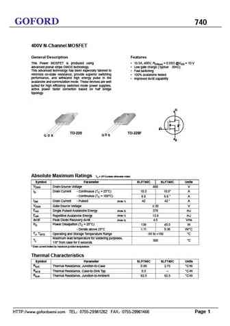
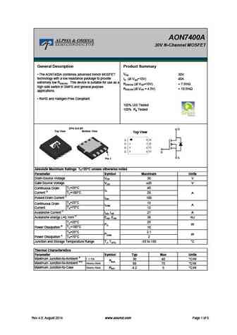
GOFORD 740 400V N-Channel MOSFET General Description Features This Power MOSFET is produced using 10.5A, 400V, RDS(on) = 0.55 @VGS = 10 V advanced planar stripe DMOS technology. Low gate charge ( typical 30nC) This advanced technology has been especially tailored to Fast switching minimize on-state resistance, provide superior switching 100% avalanche tested perform
740 f740 i740 e740 b740 d740.pdf
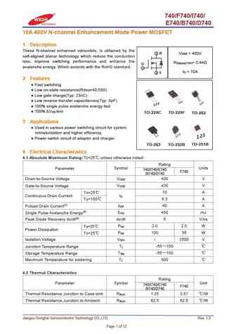
740/F740/I740/ E740/B740/D740 10A 400V N-channel Enhancement Mode Power MOSFET 1 Description These N-channel enhanced vdmosfets, is obtained by the 2 D V = 400V DSS self-aligned planar technology which reduce the conduction loss, improve switching performance and enhance the R = 0.44 DS(on)(TYP) G avalanche energy. Which accords with the RoHS standard. 1 I = 10A 3 S D 2 Featu
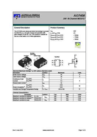
aon7405.pdf
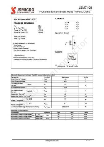
AON7405 30V P-Channel MOSFET General Description Product Summary VDS -30V The AON7405 uses advanced trench technology to provide excellent RDS(ON) with low gate charge. ID (at VGS= -10V) -50A This device is ideal for load switch and battery protection RDS(ON) (at VGS= -10V)
jcs740vc jcs740rc jcs740sc jcs740bc jcs740cc jcs740fc.pdf
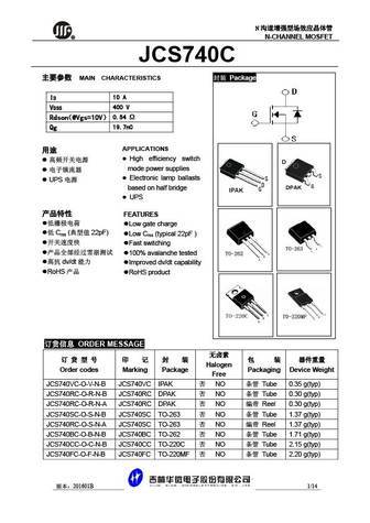
N R N-CHANNEL MOSFET JCS740C MAIN CHARACTERISTICS Package 10 A ID 400 V VDSS Rdson 0.54 @Vgs=10V 19.7nC Qg APPLICATIONS High efficiency switch mode power supplies Electronic lamp ballasts UPS based on half bridge UPS
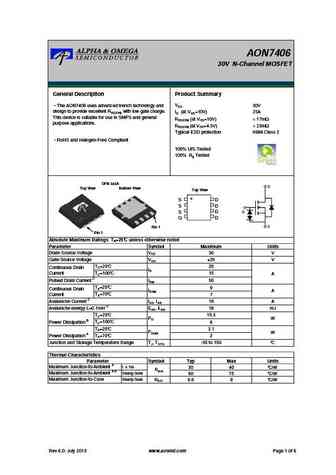
aon7408.pdf
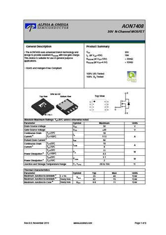
AON7408 30V N-Channel MOSFET General Description Product Summary VDS 30V The AON7408 uses advanced trench technology and design to provide excellent RDS(ON) with low gate charge. ID (at VGS=10V) 18A This device is suitable for use in general purpose RDS(ON) (at VGS=10V)
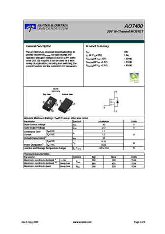
aon7406.pdf
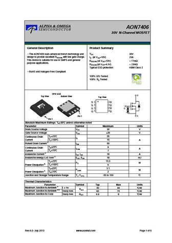
AON7406 30V N-Channel MOSFET General Description Product Summary VDS 30V The AON7406 uses advanced trench technology and design to provide excellent RDS(ON) with low gate charge. ID (at VGS=10V) 25A This device is suitable for use in SMPS and general RDS(ON) (at VGS=10V)
aon7403.pdf
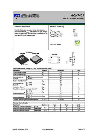
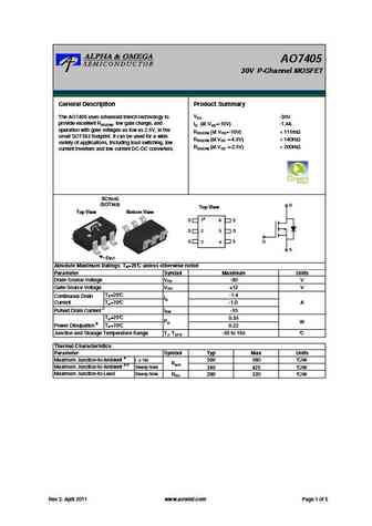
AON7403 30V P-Channel MOSFET General Description Product Summary VDS -30V The AON7403 uses advanced trench technology to provide excellent RDS(ON), and ultra-low low gate charge ID (at VGS=-10V) -29A with a 25V gate rating. This device is suitable for use as a RDS(ON) (at VGS=-10V)

svf740t svf740f.pdf

SVF740T/F_Datasheet 10A, 400V N-CHANNEL MOSFET GENERAL DESCRIPTION SVF740T/F is an N-channel enhancement mode power MOS field effect transistor which is produced using Silan proprietary F-cellTM structure VDMOS technology. The improved planar stripe cell and the improved guard ring terminal have been especially tailored to minimize on-state resistance, provide superior switching
jsm7409b.pdf
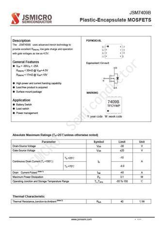
JSM7409B Plastic-Encapsulate MOSFETS PDFN3X3-8L Description The JSM7409B uses advanced trench technology to 1 8 provide excellent RDS(ON), low gate charge and operation 2 7 3 6 with gate voltages as low as 4.5V. 4 5 General Features Equivalent Cir cuit VDS = -30V,ID = -25A D RDS(ON)
aon7409.pdf
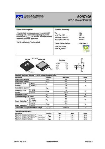
AON7409 30V P-Channel MOSFET General Description Product Summary VDS The AON7409 combines advanced trench MOSFET -30V technology with a low resistance package to provide ID (at VGS=-10V) -32A extremely low RDS(ON). This device is ideal for load switch RDS(ON) (at VGS=-10V)
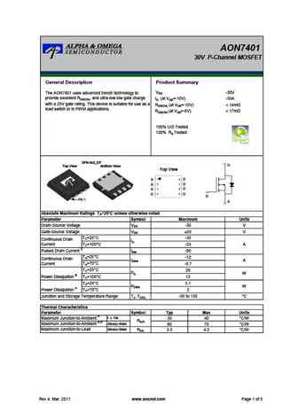
aon7401.pdf
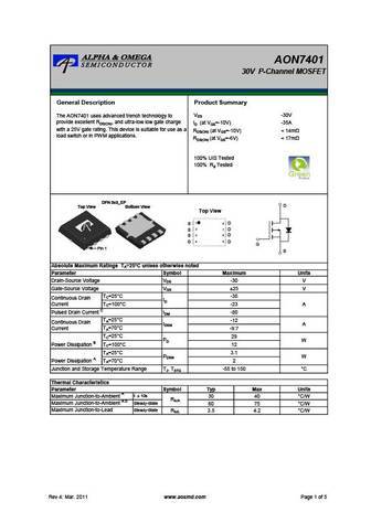
AON7401 30V P-Channel MOSFET General Description Product Summary VDS -30V The AON7401 uses advanced trench technology to provide excellent RDS(ON), and ultra-low low gate charge ID (at VGS=-10V) -35A with a 25V gate rating. This device is suitable for use as a RDS(ON) (at VGS=-10V)
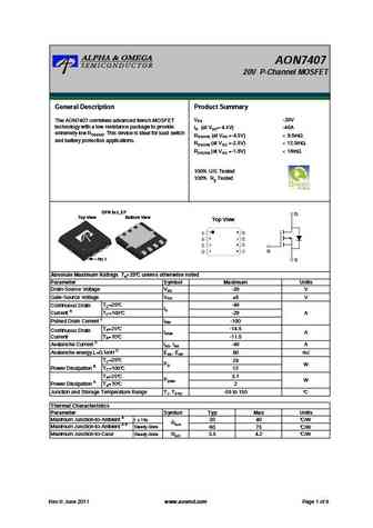
aon7407.pdf
AON7407 20V P-Channel MOSFET General Description Product Summary VDS -20V The AON7407 combines advanced trench MOSFET technology with a low resistance package to provide ID (at VGS=-4.5V) -40A extremely low RDS(ON). This device is ideal for load switch RDS(ON) (at VGS =-4.5V)
irf7403pbf.pdf
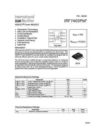
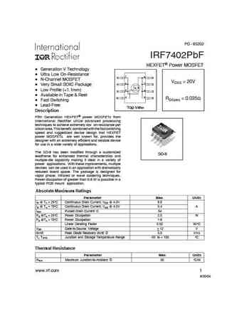
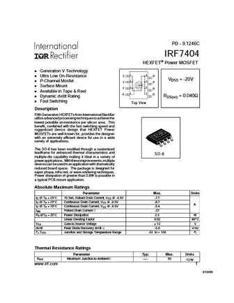
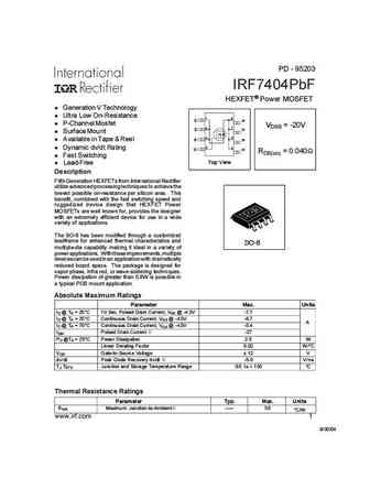
PD - 95301 IRF7403PbF HEXFET Power MOSFET l Generation V Technology A l Ultra Low On-Resistance A 1 8 S D l N-Channel Mosfet VDSS = 30V 2 7 S D l Surface Mount 3 6 l Available in Tape & Reel S D l Dynamic dv/dt Rating 4 5 G D RDS(on) = 0.022 l Fast Switching l Lead-Free Top View Description Fifth Generation HEXFETs from International Rectifier utilize advanced proc
irf7406pbf.pdf
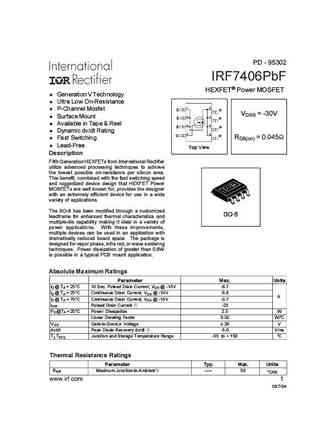
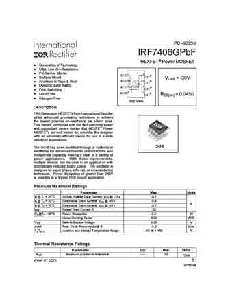
PD - 95302 IRF7406PbF HEXFET Power MOSFET l Generation V Technology l Ultra Low On-Resistance A 1 8 l P-Channel Mosfet S D VDSS = -30V 2 7 l Surface Mount S D l Available in Tape & Reel 3 6 S D l Dynamic dv/dt Rating 4 5 G D RDS(on) = 0.045 l Fast Switching l Lead-Free Top View Description Fifth Generation HEXFETs from International Rectifier utilize advanced proces
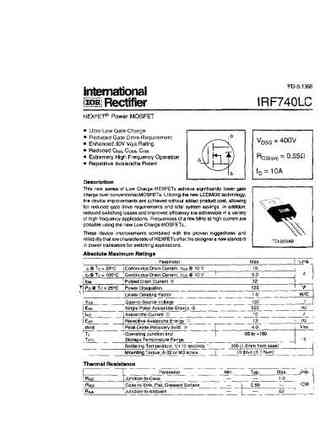
irf740lcpbf.pdf
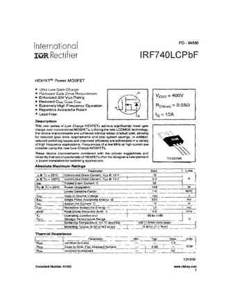
PD - 94880 IRF740LCPbF Lead-Free 12/10/03 Document Number 91052 www.vishay.com 1 IRF740LCPbF Document Number 91052 www.vishay.com 2 IRF740LCPbF Document Number 91052 www.vishay.com 3 IRF740LCPbF Document Number 91052 www.vishay.com 4 IRF740LCPbF Document Number 91052 www.vishay.com 5 IRF740LCPbF Document Number 91052 www.vishay.com 6 IRF740LCPbF Document Nu
irf7402pbf.pdf
PD - 95202 IRF7402PbF HEXFET Power MOSFET Generation V Technology A Ultra Low On-Resistance A 1 8 S D N-Channel MOSFET VDSS = 20V 2 7 S D Very Small SOIC Package Low Profile (
irfb7740.pdf
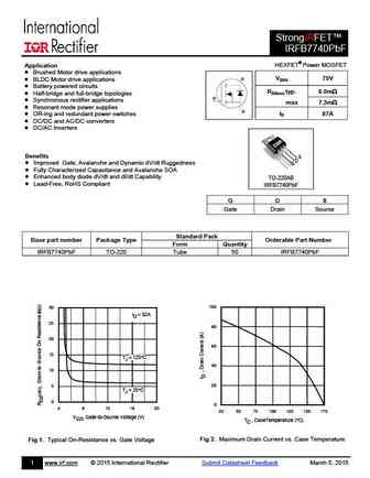
StrongIRFET IRFB7740PbF HEXFET Power MOSFET Application Brushed Motor drive applications D VDSS 75V BLDC Motor drive applications Battery powered circuits RDS(on) typ. 6.0m Half-bridge and full-bridge topologies G Synchronous rectifier applications max 7.3m Resonant mode power supplies S OR-ing and redun
irf7406gpbf.pdf
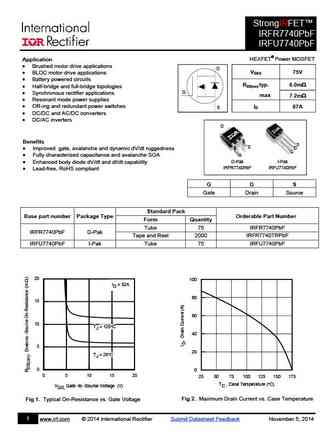
PD -96259 IRF7406GPbF HEXFET Power MOSFET l Generation V Technology l Ultra Low On-Resistance A l P-Channel Mosfet 1 8 S D l Surface Mount VDSS = -30V 2 7 S D l Available in Tape & Reel l Dynamic dv/dt Rating 3 6 S D l Fast Switching 4 5 G D l Lead-Free RDS(on) = 0.045 l Halogen-Free Top View Description Fifth Generation HEXFETs from International Rectifier utilize
irfr7740pbf irfu7740pbf.pdf
StrongIRFET IRFR7740PbF IRFU7740PbF HEXFET Power MOSFET Application Brushed motor drive applications D VDSS 75V BLDC motor drive applications Battery powered circuits RDS(on) typ. 6.0m Half-bridge and full-bridge topologies G Synchronous rectifier applications max 7.2m Resonant mode power supplies O
irf7404qpbf.pdf
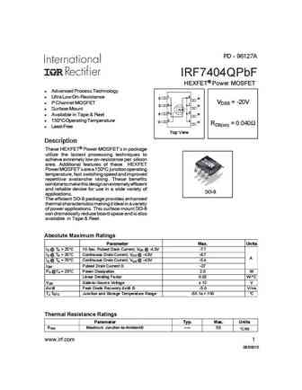
PD - 96127A IRF7404QPbF HEXFET Power MOSFET l Advanced Process Technology A 1 8 l Ultra Low On-Resistance S D VDSS = -20V l P Channel MOSFET 2 7 S D l Surface Mount 3 6 S D l Available in Tape & Reel 4 5 l 150 C Operating Temperature G D RDS(on) = 0.040 l Lead-Free Top View Description These HEXFET Power MOSFET's in package utilize the lastest processing techniqu
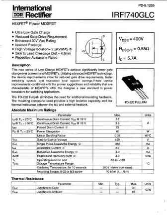
irfi740g.pdf
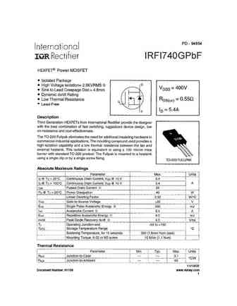
PD - 94854 IRFI740GPbF Lead-Free 11/19/03 Document Number 91156 www.vishay.com 1 IRFI740GPbF Document Number 91156 www.vishay.com 2 IRFI740GPbF Document Number 91156 www.vishay.com 3 IRFI740GPbF Document Number 91156 www.vishay.com 4 IRFI740GPbF Document Number 91156 www.vishay.com 5 IRFI740GPbF Document Number 91156 www.vishay.com 6 IRFI740GPbF TO-220 Full
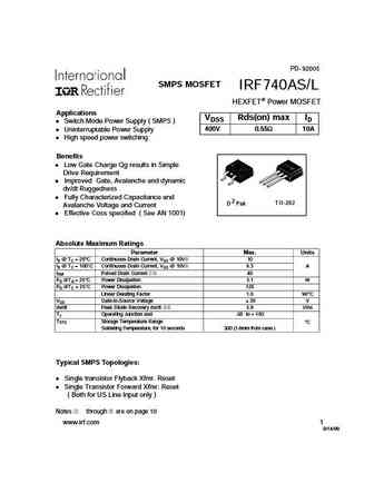
irf740as-l.pdf
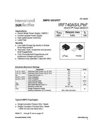
PD- 95532 SMPS MOSFET IRF740AS/LPbF HEXFET Power MOSFET Applications VDSS Rds(on) max ID l Switch Mode Power Supply ( SMPS ) l Uninterruptable Power Supply 400V 0.55 10A l High speed power switching l Lead-Free Benefits l Low Gate Charge Qg results in Simple Drive Requirement l Improved Gate, Avalanche and dynamic dv/dt Ruggedness l Fully Characterized Capacitance and D 2
irf740spbf.pdf
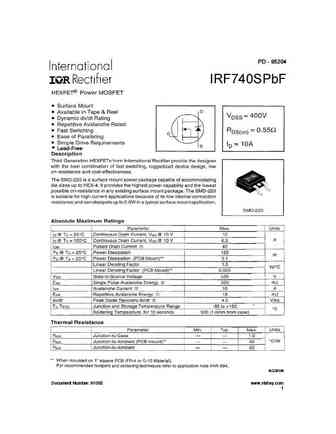
PD - 95204 IRF740SPbF Lead-Free 4/29/04 Document Number 91055 www.vishay.com 1 IRF740SPbF Document Number 91055 www.vishay.com 2 IRF740SPbF Document Number 91055 www.vishay.com 3 IRF740SPbF Document Number 91055 www.vishay.com 4 IRF740SPbF Document Number 91055 www.vishay.com 5 IRF740SPbF Document Number 91055 www.vishay.com 6 IRF740SPbF D2Pak Package Outli
irf7401pbf.pdf
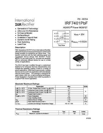
PD - 95724 IRF7401PbF HEXFET Power MOSFET l Generation V Technology l Ultra Low On-Resistance A A 1 8 l N-Channel Mosfet S D VDSS = 20V l Surface Mount 2 7 S D l Available in Tape & Reel 3 6 S D l Dynamic dv/dt Rating 4 5 G D RDS(on) = 0.022 l Fast Switching l Lead-Free Top View Description Fifth Generation HEXFETs from International Rectifier utilize advanced proc
irf740as.pdf
PD- 92005 SMPS MOSFET IRF740AS/L HEXFET Power MOSFET Applications VDSS Rds(on) max ID Switch Mode Power Supply ( SMPS ) Uninterruptable Power Supply 400V 0.55 10A High speed power switching Benefits Low Gate Charge Qg results in Simple Drive Requirement Improved Gate, Avalanche and dynamic dv/dt Ruggedness Fully Characterized Capacitance and D 2 TO-262 Pak Avalanch
irf740a.pdf
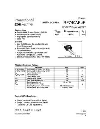
PD- 94828 SMPS MOSFET IRF740APbF HEXFET Power MOSFET Applications VDSS Rds(on) max ID l Switch Mode Power Supply ( SMPS ) l Uninterruptable Power Supply 400V 0.55 10A l High speed power switching l Lead-Free Benefits l Low Gate Charge Qg results in Simple Drive Requirement l Improved Gate, Avalanche and dynamic dv/dt Ruggedness l Fully Characterized Capacitance and Avalanch
irgp4740d.pdf
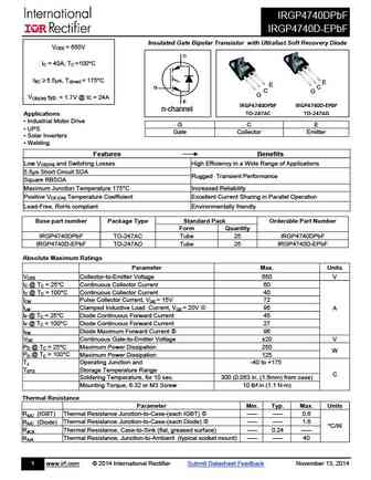
IRGP4740DPbF IRGP4740D-EPbF Insulated Gate Bipolar Transistor with Ultrafast Soft Recovery Diode VCES = 650V C IC = 40A, TC =100 C tSC 5.5 s, TJ(max) = 175 C E E G C C G G VCE(ON) typ. = 1.7V @ IC = 24A E IRGP4740DPbF IRGP4740D-EPbF n-channel TO-247AC TO-247AD Applications Industrial Motor Drive G C E UPS Gate Collector Emitter Sola
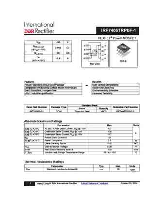
irf7404pbf-1.pdf
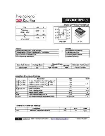
IRF7404TRPbF-1 HEXFET Power MOSFET VDS -20 V A 1 8 S D RDS(on) max 0.04 2 7 (@V = -4.5V) S D GS Qg 50 nC 3 6 S D ID 4 5 -6.7 A G D (@T = 25 C) A Top View SO-8 Features Benefits Industry-standard pinout SO-8 Package Multi-Vendor Compatibility Compatible with Existing Surface Mount Techniques Easier Manufacturing RoHS Compliant, Halogen-Free Environmentally Frie
irf7401pbf-1.pdf
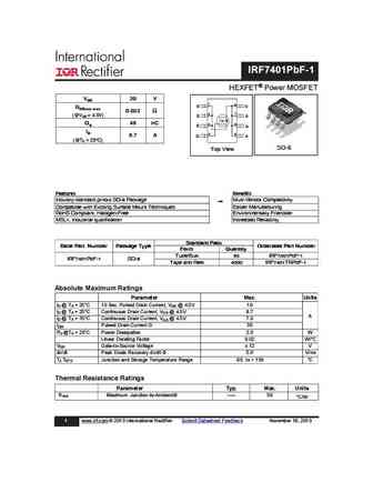
IRF7401PbF-1 HEXFET Power MOSFET VDS 20 V A A 1 8 S D RDS(on) max 0.022 2 7 (@V = 4.5V) S D GS Qg 48 nC 3 6 S D ID 4 5 8.7 A G D (@T = 25 C) A SO-8 Top View Features Benefits Industry-standard pinout SO-8 Package Multi-Vendor Compatibility Compatible with Existing Surface Mount Techniques Easier Manufacturing RoHS Compliant, Halogen-Free Environmentally Fri
irf740alpbf irf740aspbf.pdf
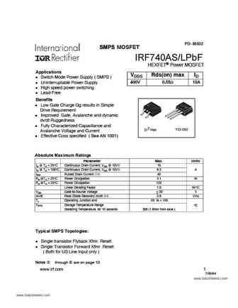
PD- 95532 SMPS MOSFET IRF740AS/LPbF HEXFET Power MOSFET Applications VDSS Rds(on) max ID l Switch Mode Power Supply ( SMPS ) l Uninterruptable Power Supply 400V 0.55 10A l High speed power switching l Lead-Free Benefits l Low Gate Charge Qg results in Simple Drive Requirement l Improved Gate, Avalanche and dynamic dv/dt Ruggedness l Fully Characterized Capacitance and 2
irf7404.pdf
PD - 9.1246C IRF7404 HEXFET Power MOSFET Generation V Technology A 1 8 S D Ultra Low On-Resistance VDSS = -20V 2 7 P-Channel Mosfet S D Surface Mount 3 6 S D Available in Tape & Reel 4 5 G D RDS(on) = 0.040 Dynamic dv/dt Rating Fast Switching Top View Description Fifth Generation HEXFETs from International Rectifier utilize advanced processing techniques to a
irf7406pbf-1.pdf
IRF7406TRPbF-1 HEXFET Power MOSFET VDS -30 V A 1 8 S D RDS(on) max 0.045 2 7 (@V = -10V) S D GS Qg (max) 59 nC 3 6 S D ID 4 5 G D -5.8 A (@T = 25 C) A SO-8 Top View Features Benefits Industry-standard pinout SO-8 Package Multi-Vendor Compatibility Compatible with Existing Surface Mount Techniques Easier Manufacturing RoHS Compliant, Halogen-Free Environment
irf7401.pdf
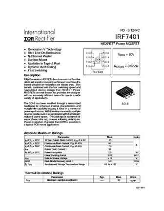
PD - 9.1244C IRF7401 HEXFET Power MOSFET Generation V Technology A A 1 8 Ultra Low On-Resistance S D VDSS = 20V 2 7 N-Channel Mosfet S D Surface Mount 3 6 S D Available in Tape & Reel 4 5 G D RDS(on) = 0.022 Dynamic dv/dt Rating Fast Switching Top View Description Fifth Generation HEXFETs from International Rectifier utilize advanced processing techniques to
irf7402.pdf
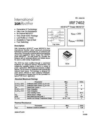
PD - 93851A IRF7402 HEXFET Power MOSFET Generation V Technology A A Ultra Low On-Resistance 1 8 S D N-Channel MOSFET VDSS = 20V 2 7 S D Very Small SOIC Package 3 6 S D Low Profile (
irf7404pbf.pdf
PD - 95203 IRF7404PbF HEXFET Power MOSFET l Generation V Technology l Ultra Low On-Resistance A 1 8 S D l P-Channel Mosfet VDSS = -20V 2 7 S D l Surface Mount 3 6 S l Available in Tape & Reel D 4 5 l Dynamic dv/dt Rating G D RDS(on) = 0.040 l Fast Switching Top View l Lead-Free Description Fifth Generation HEXFETs from International Rectifier utilize advanced proces
irf7403.pdf
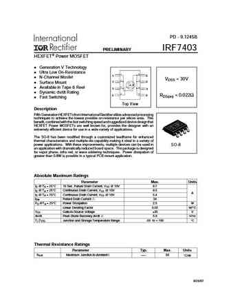
PD - 9.1245B PRELIMINARY IRF7403 HEXFET Power MOSFET Generation V Technology A Ultra Low On-Resistance A 1 8 S D N-Channel Mosfet VDSS = 30V 2 7 S D Surface Mount 3 6 Available in Tape & Reel S D Dynamic dv/dt Rating 4 5 G D RDS(on) = 0.022 Fast Switching Top View Description Fifth Generation HEXFETs from International Rectifier utilize advanced processing te
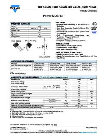
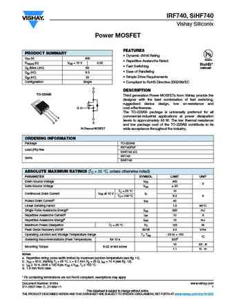
irf740.pdf
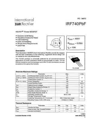
PD - 94872 IRF740PbF Lead-Free 12/5/03 Document Number 91053 www.vishay.com 1 IRF740PbF Document Number 91053 www.vishay.com 2 IRF740PbF Document Number 91053 www.vishay.com 3 IRF740PbF Document Number 91053 www.vishay.com 4 IRF740PbF Document Number 91053 www.vishay.com 5 IRF740PbF Document Number 91053 www.vishay.com 6 IRF740PbF TO-220AB Package Outline
irl5nj7404.pdf
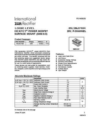
PD-94052B LOGIC LEVEL IRL5NJ7404 HEXFET POWER MOSFET 20V, P-CHANNEL SURFACE MOUNT (SMD-0.5) Product Summary Part Number BVDSS RDS(on) ID IRL5NJ7404 -20V 0.04 -11A SMD-0.5 Fifth Generation HEXFET power MOSFETs from International Rectifier utilize advanced processing Features techniques to achieve the lowest possible on-resistance n Logic Level Gate Drive per silicon unit a
irf7406.pdf
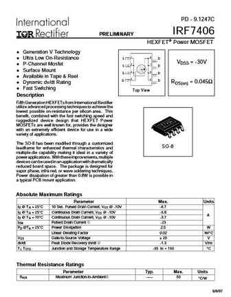
PD - 9.1247C IRF7406 PRELIMINARY HEXFET Power MOSFET Generation V Technology A 1 8 Ultra Low On-Resistance S D VDSS = -30V 2 7 P-Channel Mosfet S D Surface Mount 3 6 S D Available in Tape & Reel 4 5 G D RDS(on) = 0.045 Dynamic dv/dt Rating Fast Switching Top V iew Description Fifth Generation HEXFETs from International Rectifier utilize advanced processing te
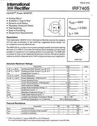
irf740s.pdf
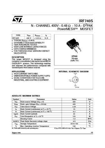
IRF740S N - CHANNEL 400V - 0.48 - 10A- D2PAK PowerMESH MOSFET TYPE VDSS RDS(on) ID IRF740S 400 V
irf740.pdf
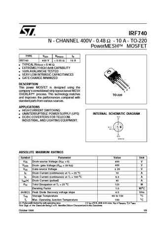
IRF740 N - CHANNEL 400V - 0.48 - 10 A - TO-220 PowerMESH MOSFET TYPE VDSS RDS(on) ID IRF740 400 V
2sk1740.pdf

Ordering number EN4112 N-Channel Junction Silicon FET 2SK1740 HF amplifiers low frequency amplifiers analog switches Features Package Dimensions Adoption of FBET process. unit mm Large yfs . 2050A Small Ciss. [2SK1740] Small-sized package permitting 2SK1740-applied 0.4 0.16 sets to be made small and slim. 3 0 to 0.1 1 0.95 2 0.95 1.9 2.9 1 Source 2
2sb740.pdf

To all our customers Regarding the change of names mentioned in the document, such as Hitachi Electric and Hitachi XX, to Renesas Technology Corp. The semiconductor operations of Mitsubishi Electric and Hitachi were transferred to Renesas Technology Corporation on April 1st 2003. These operations include microcomputer, logic, analog and discrete devices, and memory chips other than DRAM
2sk740.pdf
To our customers, Old Company Name in Catalogs and Other Documents On April 1st, 2010, NEC Electronics Corporation merged with Renesas Technology Corporation, and Renesas Electronics Corporation took over all the business of both companies. Therefore, although the old company name remains in this document, it is a valid Renesas Electronics document. We appreciate your understanding.
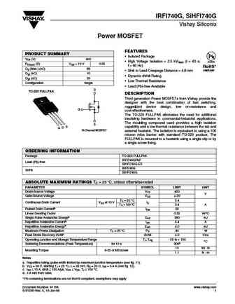
irfw740b irfi740b.pdf
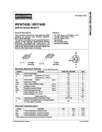
November 2001 IRFW740B / IRFI740B 400V N-Channel MOSFET General Description Features These N-Channel enhancement mode power field effect 10A, 400V, RDS(on) = 0.54 @VGS = 10 V transistors are produced using Fairchild s proprietary, Low gate charge ( typical 41 nC) planar, DMOS technology. Low Crss ( typical 35 pF) This advanced technology has been especially tailored to
2sk3740-zk.pdf
To our customers, Old Company Name in Catalogs and Other Documents On April 1st, 2010, NEC Electronics Corporation merged with Renesas Technology Corporation, and Renesas Electronics Corporation took over all the business of both companies. Therefore, although the old company name remains in this document, it is a valid Renesas Electronics document. We appreciate your understanding.
2sk3740.pdf
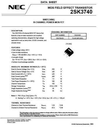
DATA SHEET MOS FIELD EFFECT TRANSISTOR 2SK3740 SWITCHING N-CHANNEL POWER MOS FET DESCRIPTION ORDERING INFORMATION The 2SK3740 is N-channel MOS FET device that PART NUMBER PACKAGE features a low on-state resistance and excellent switching characteristics, designed for high voltage 2SK3740-ZK TO-263 (MP-25ZK) applications such as lamp drive, DC/DC converter, and actuator driv
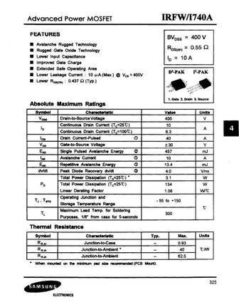
irfs740a.pdf
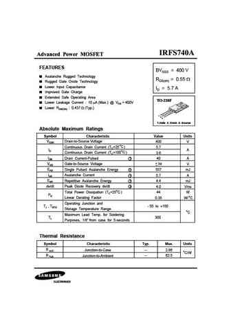
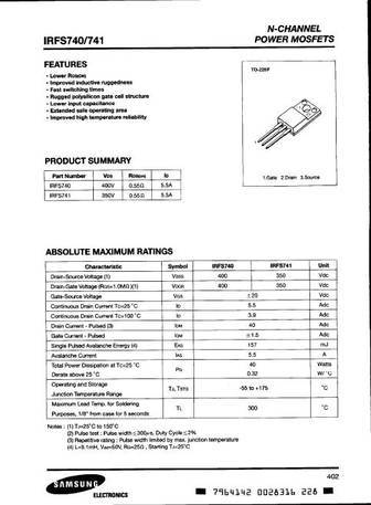
Advanced Power MOSFET FEATURES BVDSS = 400 V Avalanche Rugged Technology RDS(on) = 0.55 Rugged Gate Oxide Technology Lower Input Capacitance ID = 5.7 A Improved Gate Charge Extended Safe Operating Area Lower Leakage Current 10 A (Max.) @ VDS = 400V Lower RDS(ON) 0.437 (Typ.) 1 2 3 1.Gate 2. Drain 3. Source Absolute Maximum Ratings Symbol Characteristic Val
irf740a.pdf
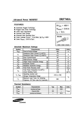
Advanced Power MOSFET FEATURES BVDSS = 400 V Avalanche Rugged Technology RDS(on) = 0.55 Rugged Gate Oxide Technology Lower Input Capacitance ID = 10 A Improved Gate Charge Extended Safe Operating Area Lower Leakage Current 10 A (Max.) @ VDS = 400V Lower RDS(ON) 0.437 (Typ.) 1 2 3 1.Gate 2. Drain 3. Source Absolute Maximum Ratings Symbol Characteristic Va

irfw740a.pdf
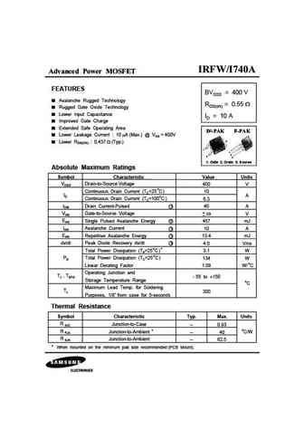
Advanced Power MOSFET FEATURES BVDSS = 400 V Avalanche Rugged Technology RDS(on) = 0.55 Rugged Gate Oxide Technology Lower Input Capacitance ID = 10 A Improved Gate Charge Extended Safe Operating Area Lower Leakage Current 10 A (Max.) @ VDS = 400V 2 Lower RDS(ON) 0.437 (Typ.) 1 1 2 3 3 1. Gate 2. Drain 3. Source Absolute Maximum Ratings Symbol Cha
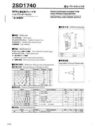
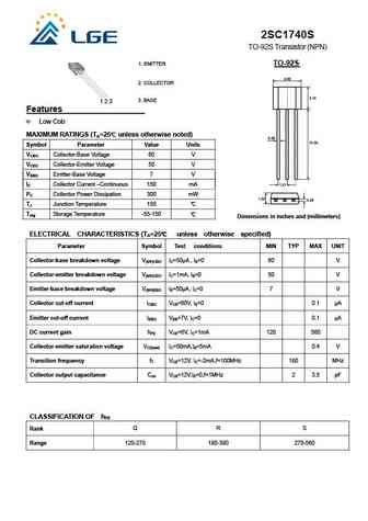
2sc2412k 2sc4081 2sc4617 2sc5658 2sc1740s.pdf
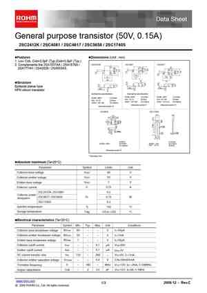
General purpose transistor (50V, 0.15A) 2SC2412K / 2SC4081 / 2SC4617 / 2SC5658 / 2SC1740S Features Dimensions (Unit mm) 1. Low Cob. Cob=2.0pF (Typ.)Cob=2.0pF (Typ.) 2SC2412K 2SC4081 2SC4617 2. Complements the 2SA1037AK / 2SA1576A / 2SA1774H / 2SA2029 / 2SA933AS. (1) (2) (3) 1.25 1.6 0.8 2.1 2.8 1.6 Structure Epitaxial planar type 0.1Min. 0.1Min. 0.3Min. NPN
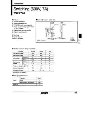
2sk2740.pdf
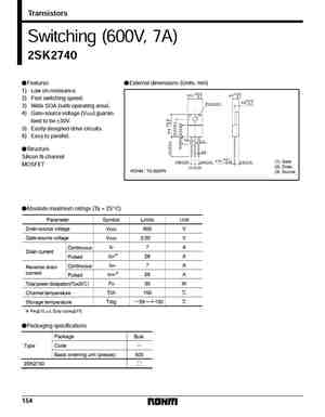
Transistors Switching (600V, 7A) 2SK2740 FFeatures FExternal dimensions (Units mm) 1) Low on-resistance. 2) Fast switching speed. 3) Wide SOA (safe operating area). 4) Gate-source voltage (VGSS) guaran- teed to be 30V. 5) Easily designed drive circuits. 6) Easy to parallel. FStructure Silicon N-channel MOSFET FAbsolute maximum ratings (Ta = 25_C) FPackaging specifications 15
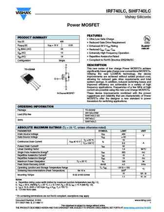
irf740b.pdf
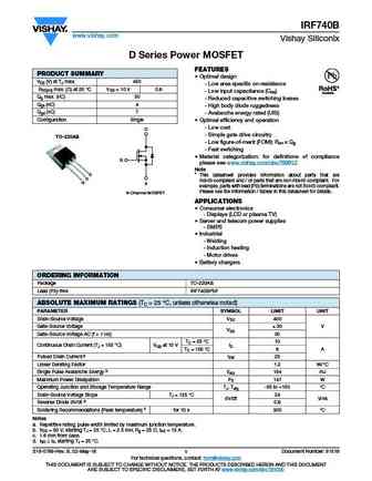
IRF740B www.vishay.com Vishay Siliconix D Series Power MOSFET FEATURES PRODUCT SUMMARY Optimal design VDS (V) at TJ max. 450 - Low area specific on-resistance RDS(on) max. ( ) at 25 C VGS = 10 V 0.6 - Low input capacitance (Ciss) Available Qg max. (nC) 30 - Reduced capacitive switching losses Qgs (nC) 4 - High body diode ruggedness Qgd (nC) 7 - Avalanche energy rated (U
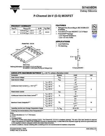
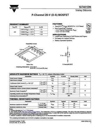
si7409adn.pdf
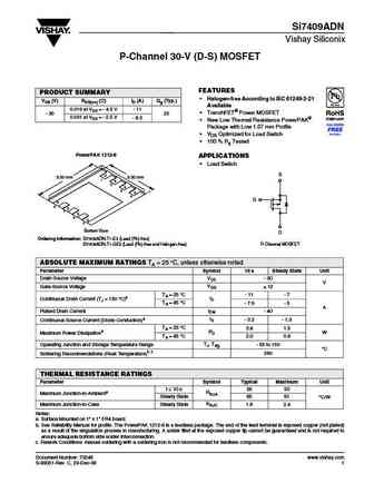
Si7409ADN Vishay Siliconix P-Channel 30-V (D-S) MOSFET FEATURES PRODUCT SUMMARY Halogen-free According to IEC 61249-2-21 VDS (V) RDS(on) ( )ID (A) Qg (Typ.) Available 0.019 at VGS = - 4.5 V - 11 TrenchFET Power MOSFET - 30 25 0.031 at VGS = - 2.5 V - 8.5 New Low Thermal Resistance PowerPAK Package with Low 1.07 mm Profile VDS Optimized for Load Switch
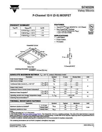
si7405bdn.pdf

New Product Si7405BDN Vishay Siliconix P-Channel 12-V (D-S) MOSFET FEATURES PRODUCT SUMMARY Halogen-free Option Available VDS (V) RDS(on) ( )ID (A) Qg (Typ.) TrenchFET Power MOSFET 0.013 at VGS = - 4.5 V - 16a RoHS 0.017 at VGS = - 2.5 V - 12 - 16a 46 nC COMPLIANT APPLICATIONS 0.024 at VGS = - 1.8 V - 16a Load Switch, PA Switch and Power Switch for Portab
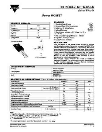
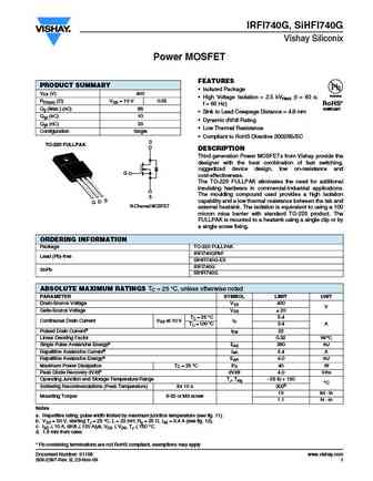
irfi740g sihfi740g.pdf
IRFI740G, SiHFI740G Vishay Siliconix Power MOSFET FEATURES PRODUCT SUMMARY Isolated Package VDS (V) 400 High Voltage Isolation = 2.5 kVRMS (t = 60 s; Available RDS(on) ( )VGS = 10 V 0.55 f = 60 Hz) RoHS* Qg (Max.) (nC) 66 COMPLIANT Sink to Lead Creepage Distance = 4.8 mm Qgs (nC) 10 Dynamic dV/dt Rating Qgd (nC) 33 Low Thermal Resistance Configuration Sin
irf740a sihf740a.pdf
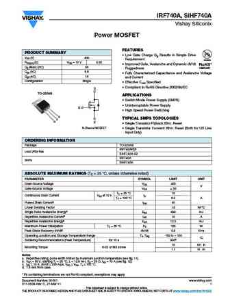
IRF740A, SiHF740A Vishay Siliconix Power MOSFET FEATURES PRODUCT SUMMARY Low Gate Charge Qg Results in Simple Drive VDS (V) 400 Requirement Available RDS(on) ( )VGS = 10 V 0.55 Improved Gate, Avalanche and Dynamic dV/dt RoHS* Qg (Max.) (nC) 36 COMPLIANT Ruggedness Qgs (nC) 9.9 Fully Characterized Capacitance and Avalanche Voltage Qgd (nC) 16 and Current Configur
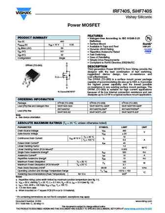
irf740spbf sihf740s.pdf

IRF740S, SiHF740S Vishay Siliconix Power MOSFET FEATURES PRODUCT SUMMARY Halogen-free According to IEC 61249-2-21 Definition VDS (V) 400 Surface Mount RDS(on) ( )VGS = 10 V 0.55 Available in Tape and Reel Qg (Max.) (nC) 63 Dynamic dV/dt Rating Qgs (nC) 9.0 Repetitive Avalanche Rated Fast Switching Qgd (nC) 32 Ease of Paralleling Configuration Sin
irf740lc irf740lcpbf sihf740lc.pdf

IRF740LC, SiHF740LC Vishay Siliconix Power MOSFET FEATURES PRODUCT SUMMARY Ultra Low Gate Charge VDS (V) 400 Reduced Gate Drive Requirement Available RDS(on) ( )VGS = 10 V 0.55 Enhanced 30 V VGS Rating RoHS* COMPLIANT Qg (Max.) (nC) 39 Reduced Ciss, Coss, Crss Qgs (nC) 10 Extremely High Frequency Operation Qgd (nC) 19 Repetitive Avalanche Rated Comp
irfi740glc sihfi740glc.pdf
IRFI740GLC, SiHFI740GLC Vishay Siliconix Power MOSFET FEATURES PRODUCT SUMMARY Ultra Low Gate Charge VDS (V) 400 Reduced Gate Drive Requirement Available RDS(on) ( )VGS = 10 V 0.55 Enhanced 30 V VGS Rating RoHS* Isolated Package Qg (Max.) (nC) 39 COMPLIANT High Voltage Isolation = 2.5 kVRMS (t = 60 s, Qgs (nC) 10 f = 60 Hz) Qgd (nC) 19 Sink to Lead C
si7405dn.pdf
Si7405DN Vishay Siliconix P-Channel 12-V (D-S) MOSFET FEATURES PRODUCT SUMMARY TrenchFET Power MOSFETS 1.8-V Rated VDS (V) rDS(on) ( )ID (A) Pb-free New PowerPAK Package Available 0.016 at VGS = 4.5 V 13 Low Thermal Resistance, RthJC RoHS* Low 1.07-mm Profile 0.022 at VGS = 2.5 V 11 12 COMPLIANT 0.028 at VGS = 1.8 V 9.8 APPL
si7407dn.pdf
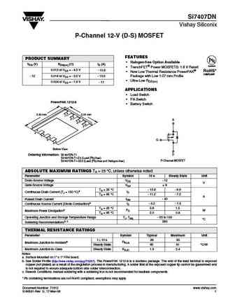
Si7407DN Vishay Siliconix P-Channel 12-V (D-S) MOSFET FEATURES PRODUCT SUMMARY Halogen-free Option Available VDS (V) RDS(on) ( )ID (A) Available TrenchFET Power MOSFETS 1.8 V Rated 0.012 at VGS = - 4.5 V - 15.6 RoHS* New Low Thermal Resistance PowerPAK COMPLIANT 0.016 at VGS = - 2.5 V - 12 - 13.5 Package with Low 1.07 mm Profile Ultra-Low RDS(on) 0.
irf740as sihf740as irf740al sihf740al.pdf

IRF740AS, SiHF740AS, IRF740AL, SiHF740AL Vishay Siliconix Power MOSFET FEATURES PRODUCT SUMMARY Halogen-free According to IEC 61249-2-21 VDS (V) 400 Definition RDS(on) ( )VGS = 10 V 0.55 Low Gate Charge Qg Results in Simple Drive Requirement Qg (Max.) (nC) 36 Improved Gate, Avalanche and Dynamic dV/dt Qgs (nC) 9.9 Ruggedness Qgd (nC) 16 Fully Characterized Capac
si7402dn.pdf
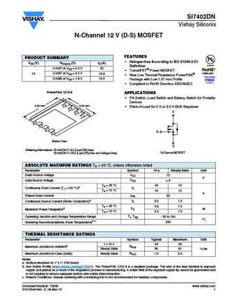
Si7402DN Vishay Siliconix N-Channel 12 V (D-S) MOSFET FEATURES PRODUCT SUMMARY Halogen-free According to IEC 61249-2-21 VDS (V) RDS(on) ( )ID (A) Definition 0.0057 at VGS = 4.5 V 20 TrenchFET Power MOSFET 0.0067 at VGS = 2.5 V 12 18.8 New Low Thermal Resistance PowerPAK 0.0085 at VGS = 1.8 V 16.5 Package with Low 1.07 mm Profile Compliant to RoHS D
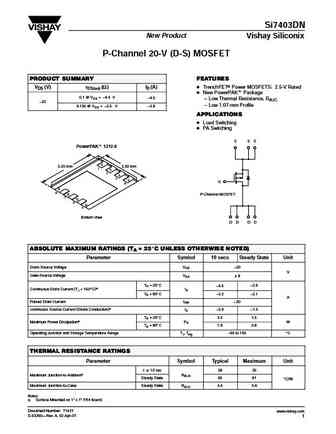
si7403bdn.pdf
Si7403BDN Vishay Siliconix P-Channel 20-V (D-S) MOSFET FEATURES PRODUCT SUMMARY Halogen-free According to IEC 61249-2-21 VDS (V) RDS(on) ( )ID (A) Qg (Typ.) Available 0.074 at VGS = - 4.5 V - 8c TrenchFET Power MOSFET 2.5 V Rated - 20 5.6 nC 0.110 at VGS = - 2.5 V - 7.4 PowerPAK Package - Low Thermal Resistance - Low 1.07 mm Profile APPLICATIONS PowerPAK
sihf740al sihf740as.pdf
IRF740AS, SiHF740AS, IRF740AL, SiHF740AL Vishay Siliconix Power MOSFET FEATURES PRODUCT SUMMARY Halogen-free According to IEC 61249-2-21 VDS (V) 400 Definition RDS(on) ( )VGS = 10 V 0.55 Low Gate Charge Qg Results in Simple Drive Requirement Qg (Max.) (nC) 36 Improved Gate, Avalanche and Dynamic dV/dt Qgs (nC) 9.9 Ruggedness Qgd (nC) 16 Fully Characterized Capac
irf740 sihf740.pdf
IRF740, SiHF740 Vishay Siliconix Power MOSFET FEATURES PRODUCT SUMMARY Dynamic dV/dt Rating VDS (V) 400 Available Repetitive Avalanche Rated RDS(on) ( )VGS = 10 V 0.55 RoHS* Fast Switching Qg (Max.) (nC) 63 COMPLIANT Ease of Paralleling Qgs (nC) 9.0 Qgd (nC) 32 Simple Drive Requirements Configuration Single Compliant to RoHS Directive 2002/95/EC D DES
si7405bd.pdf
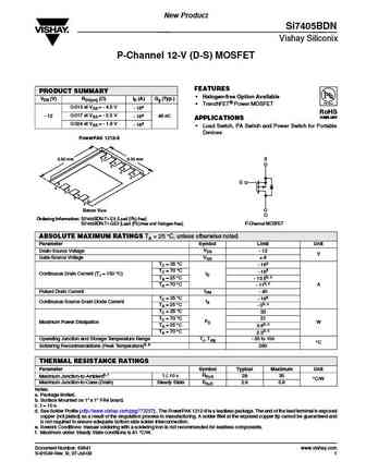
New Product Si7405BDN Vishay Siliconix P-Channel 12-V (D-S) MOSFET FEATURES PRODUCT SUMMARY Halogen-free Option Available VDS (V) RDS(on) ( )ID (A) Qg (Typ.) TrenchFET Power MOSFET 0.013 at VGS = - 4.5 V - 16a RoHS 0.017 at VGS = - 2.5 V - 12 - 16a 46 nC COMPLIANT APPLICATIONS 0.024 at VGS = - 1.8 V - 16a Load Switch, PA Switch and Power Switch for Portab
si7401dn.pdf
Si7401DN Vishay Siliconix P-Channel 20-V (D-S) MOSFET FEATURES PRODUCT SUMMARY TrenchFET Power MOSFETS 1.8-V Rated VDS (V) rDS(on) ( )ID (A) Pb-free New PowerPAK Package Available 0.021 at VGS = 4.5 V 11 Low Thermal Resistance, RthJC RoHS* Low 1.07-mm Profile 0.028 at VGS = 2.5 V 9.8 20 COMPLIANT 0.034 at VGS = 1.8 V 8.9 APPL
irf740lc sihf740lc.pdf
IRF740LC, SiHF740LC Vishay Siliconix Power MOSFET FEATURES PRODUCT SUMMARY Ultra Low Gate Charge VDS (V) 400 Reduced Gate Drive Requirement Available RDS(on) ( )VGS = 10 V 0.55 Enhanced 30 V VGS Rating RoHS* COMPLIANT Qg (Max.) (nC) 39 Reduced Ciss, Coss, Crss Qgs (nC) 10 Extremely High Frequency Operation Qgd (nC) 19 Repetitive Avalanche Rated Comp
si7404dn.pdf
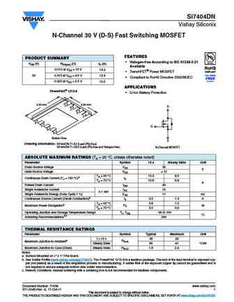
Si7404DN Vishay Siliconix N-Channel 30 V (D-S) Fast Switching MOSFET FEATURES PRODUCT SUMMARY Halogen-free According to IEC 61249-2-21 VDS (V) RDS(on) ( )ID (A) Available 0.013 at VGS = 10 V 13.3 TrenchFET Power MOSFET 0.015 at VGS = 4.5 V 30 12.4 Compliant to RoHS Directive 2002/95/EC 0.022 at VGS = 2.5 V 10.2 APPLICATIONS PowerPAK 1212-8 Li-lon
sihfi740glc.pdf

IRFI740GLC, SiHFI740GLC Vishay Siliconix Power MOSFET FEATURES PRODUCT SUMMARY Ultra Low Gate Charge VDS (V) 400 Reduced Gate Drive Requirement Available RDS(on) ( )VGS = 10 V 0.55 Enhanced 30 V VGS Rating RoHS* Isolated Package Qg (Max.) (nC) 39 COMPLIANT High Voltage Isolation = 2.5 kVRMS (t = 60 s, Qgs (nC) 10 f = 60 Hz) Qgd (nC) 19 Sink to Lead C
irf740s sihf740s.pdf
IRF740S, SiHF740S Vishay Siliconix Power MOSFET FEATURES PRODUCT SUMMARY Halogen-free According to IEC 61249-2-21 Definition VDS (V) 400 Surface Mount RDS(on) ( )VGS = 10 V 0.55 Available in Tape and Reel Qg (Max.) (nC) 63 Dynamic dV/dt Rating Qgs (nC) 9.0 Repetitive Avalanche Rated Fast Switching Qgd (nC) 32 Ease of Paralleling Configuration Sin
sihfi740g.pdf
IRFI740G, SiHFI740G Vishay Siliconix Power MOSFET FEATURES PRODUCT SUMMARY Isolated Package VDS (V) 400 Available High Voltage Isolation = 2.5 kVRMS (t = 60 s; RDS(on) ( )VGS = 10 V 0.55 f = 60 Hz) RoHS* Qg (Max.) (nC) 66 COMPLIANT Sink to Lead Creepage Distance = 4.8 mm Qgs (nC) 10 Dynamic dV/dt Rating Qgd (nC) 33 Low Thermal Resistance Configuration Singl
si7403dn.pdf
Si7403DN New Product Vishay Siliconix P-Channel 20-V (D-S) MOSFET PRODUCT SUMMARY FEATURES D TrenchFETr Power MOSFETS 2.5-V Rated VDS (V) rDS(on) (W) ID (A) D New PowerPAKt Package 0.1 @ VGS = 4.5 V 4.5 Low Thermal Resistance, RthJC 20 Low 1.07-mm Profile 0.135 @ VGS = 2.5 V 3.8 APPLICATIONS D Load Switching D PA Switching S S S PowerPAKt 1212-8 S 3.3
irf740apbf sihf740a.pdf

IRF740A, SiHF740A Vishay Siliconix Power MOSFET FEATURES PRODUCT SUMMARY Low Gate Charge Qg Results in Simple Drive VDS (V) 400 Requirement Available RDS(on) ( )VGS = 10 V 0.55 Improved Gate, Avalanche and Dynamic dV/dt RoHS* Qg (Max.) (nC) 36 COMPLIANT Ruggedness Qgs (nC) 9.9 Fully Characterized Capacitance and Avalanche Voltage Qgd (nC) 16 and Current Configur
irf740pbf sihf740.pdf

IRF740, SiHF740 Vishay Siliconix Power MOSFET FEATURES PRODUCT SUMMARY Dynamic dV/dt Rating VDS (V) 400 Available Repetitive Avalanche Rated RDS(on) ( )VGS = 10 V 0.55 RoHS* Fast Switching Qg (Max.) (nC) 63 COMPLIANT Ease of Paralleling Qgs (nC) 9.0 Qgd (nC) 32 Simple Drive Requirements Configuration Single Compliant to RoHS Directive 2002/95/EC D DES
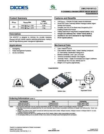
dmg7408sfg.pdf
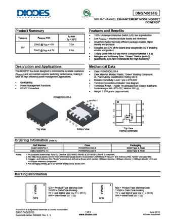
DMG7408SFG 30V N-CHANNEL ENHANCEMENT MODE MOSFET POWERDI Product Summary Features and Benefits 100% Unclamped Inductive Switch (UIS) test in production ID max V(BR)DSS RDS(ON) max Low RDS(ON) ensures on state losses are minimized TA = 25 C Small form factor thermally efficient package enables higher 23m @ VGS = 10V 7.0A density end products 30V O
dmg7401sfg.pdf
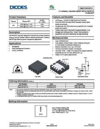
DMG7401SFG P-CHANNEL ENHANCEMENT MODE MOSFET POWERDI Product Summary Features and Benefits ID max Low RDS(ON) ensures on state losses are minimized V(BR)DSS RDS(ON) max TA = +25 C Small form factor thermally efficient package enables higher density end products 13m @ VGS = -10V -9.8A -30V Occupies just 33% of the board area occupied by SO-8 enabling
bfp740f.pdf
BFP740F Low Noise Silicon Germanium Bipolar RF Transistor Data Sheet Revision 2.0, 2015-03-12 RF & Protection Devices Edition 2015-03-12 Published by Infineon Technologies AG 81726 Munich, Germany 2015 Infineon Technologies AG All Rights Reserved. Legal Disclaimer The information given in this document shall in no event be regarded as a guarantee of conditions or characteristi
bfp740fesd.pdf
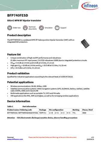
BFP740FESD SiGe C NPN RF bipolar transistor Product description The BFP740FESD is a wideband NPN RF heterojunction bipolar transistor (HBT) with an integrated ESD protection. Feature list Unique combination of high end RF performance and robustness 21 dBm maximum RF input power, 2 kV ESD robustness (HBM) due to integrated protection circuits NFmin = 0.6 dB at 2.4 GHz and 0.8 dB
bfp740.pdf
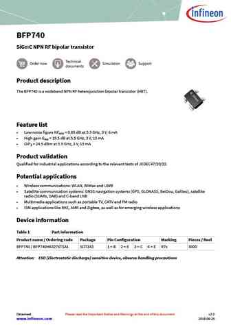
BFP740 SiGe C NPN RF bipolar transistor Product description The BFP740 is a wideband NPN RF heterojunction bipolar transistor (HBT). Feature list Low noise figure NFmin = 0.85 dB at 5.5 GHz, 3 V, 6 mA High gain Gms = 19.5 dB at 5.5 GHz, 3 V, 15 mA OIP3 = 24.5 dBm at 5.5 GHz, 3 V, 15 mA Product validation Qualified for industrial applications according to the relevant tests
bfr740el3.pdf
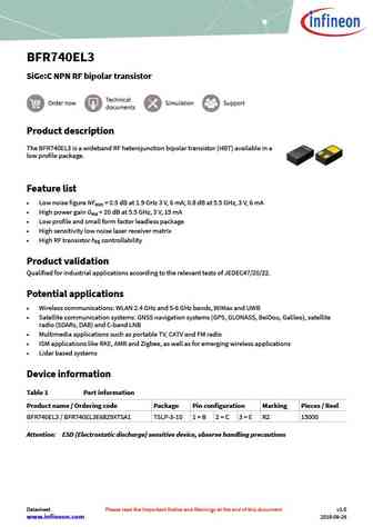
BFR740EL3 SiGe C NPN RF bipolar transistor Product description The BFR740EL3 is a wideband RF heterojunction bipolar transistor (HBT) available in a low profile package. Feature list Low noise figure NFmin = 0.5 dB at 1.9 GHz 3 V, 6 mA; 0.8 dB at 5.5 GHz, 3 V, 6 mA High power gain Gms = 20 dB at 5.5 GHz, 3 V, 15 mA Low profile and small form factor leadless package High
bfr740l3rh.pdf
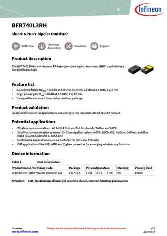
BFR740L3RH SiGe C NPN RF bipolar transistor Product description The BFR740L3RH is a wideband RF heterojunction bipolar transistor (HBT) available in a low profile package. Feature list Low noise figure NFmin = 0.5 dB at 1.9 GHz 3 V, 6 mA; 0.8 dB at 5.5 GHz, 3 V, 6 mA High power gain Gms = 20 dB at 5.5 GHz, 3 V, 15 mA Low profile and small form factor leadless package Produc
bts740s2.pdf
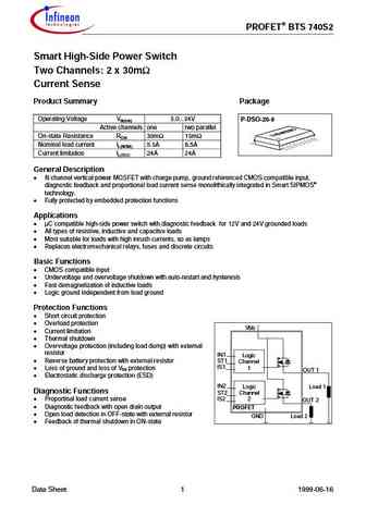
PROFET BTS 740S2 Smart High-Side Power Switch Two Channels 2 x 30m Current Sense Product Summary Package Operating Voltage Vbb(on) 5.0...34V P-DSO-20-9 Active channels one two parallel On-state Resistance RON 30m 15m Nominal load current IL(NOM) 5.5A 8.5A Current limitation IL(SCr) 24A 24A General Description N channel vertical power MOSFET with charge pump, ground
bfp740esd.pdf
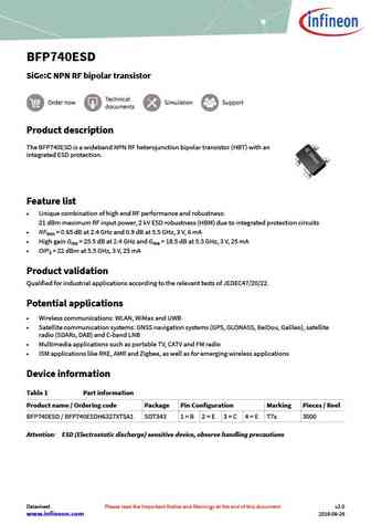
BFP740ESD SiGe C NPN RF bipolar transistor Product description The BFP740ESD is a wideband NPN RF heterojunction bipolar transistor (HBT) with an integrated ESD protection. Feature list Unique combination of high end RF performance and robustness 21 dBm maximum RF input power, 2 kV ESD robustness (HBM) due to integrated protection circuits NFmin = 0.65 dB at 2.4 GHz and 0.9 dB
2sc1740s-q-r-s.pdf
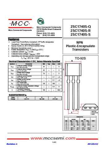
MCC Micro Commercial Components 2SC1740S-Q TM 20736 Marilla Street Chatsworth Micro Commercial Components CA 91311 2SC1740S-R Phone (818) 701-4933 2SC1740S-S Fax (818) 701-4939 Features Lead Free Finish/Rohs Compliant ("P"Suffix designates NPN Compliant. See ordering information) Epoxy meets UL 94 V-0 flammability rating Plastic-Encapsulate Moisture Sensitivity
bc33716bu bc33716ta bc33716tfr bc33725bu bc33725ta bc33725tar bc33725tf bc33725tfr bc33740bu bc33740ta bc33825ta.pdf

bc327bu bc32716bu bc32716ta bc32725bu bc32725ta bc32740bu bc32740ta.pdf

Is Now Part of To learn more about ON Semiconductor, please visit our website at www.onsemi.com Please note As part of the Fairchild Semiconductor integration, some of the Fairchild orderable part numbers will need to change in order to meet ON Semiconductor s system requirements. Since the ON Semiconductor product management systems do not have the ability to manage part nomenclatur
bc327 bc32716 bc32725 bc32740.pdf
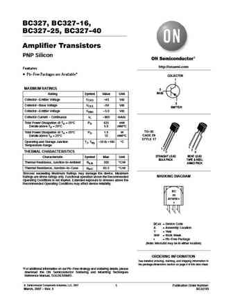
BC327, BC327-16, BC327-25, BC327-40 Amplifier Transistors PNP Silicon http //onsemi.com Features Pb-Free Packages are Available* COLLECTOR 1 MAXIMUM RATINGS 2 BASE Rating Symbol Value Unit Collector -Emitter Voltage VCEO -45 Vdc 3 Collector -Base Voltage VCES -50 Vdc EMITTER Collector -Emitter Voltage VEBO -5.0 Vdc Collector Current - Continuous IC -800 mAdc Total Power D
uf740.pdf

UNISONIC TECHNOLOGIES CO., LTD UF740 Power MOSFET 10A, 400V, 0.55 N-CHANNEL POWER MOSFET 1 1 TO-220 TO-220F DESCRIPTION The N-Channel enhancement mode silicon gate power MOSFET is designed for high voltage, high speed power switching 1 applications such as switching regulators, switching converters, 1 solenoid, motor drivers, relay drivers. TO-220F1 TO-220F2 FEAT
ut7401.pdf
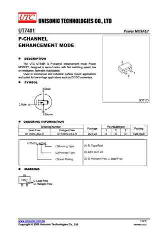
UNISONIC TECHNOLOGIES CO., LTD UT7401 Power MOSFET P-CHANNEL ENHANCEMENT MODE DESCRIPTION The UTC UT7401 is P-channel enhancement mode Power MOSFET, designed in serried ranks. with fast switching speed, low on-resistance, favorable stabilization. Used in commercial and industrial surface mount applications and suited for low voltage applications such as DC/DC converters.
uf740l-ta3-t uf740g-ta3-t uf740l-tf1-t uf740g-tf1-t uf740l-tf2-t uf740g-tf2-t uf740l-tf3-t uf740g-tf3-t uf740l-tq2-t uf740g-tq2-t uf740l-tq2-r uf740g-tq2-r.pdf
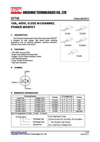
UNISONIC TECHNOLOGIES CO., LTD UF740 Power MOSFET 10A, 400V, 0.55 N-CHANNEL POWER MOSFET 1 1 TO-220 TO-220F DESCRIPTION The N-Channel enhancement mode silicon gate power MOSFET is designed for high voltage, high speed power switching 1 applications such as switching regulators, switching converters, 1 solenoid, motor drivers, relay drivers. TO-220F1 TO-220F2 FEAT
2sa1740.pdf
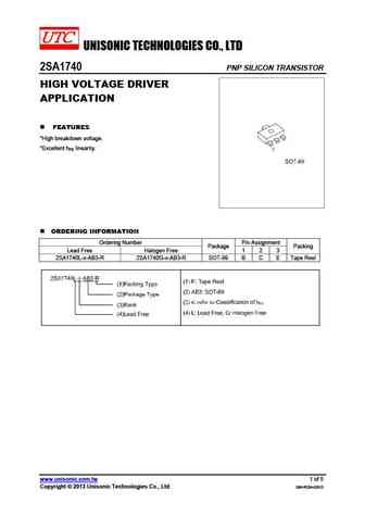
UNISONIC TECHNOLOGIES CO., LTD 2SA1740 PNP SILICON TRANSISTOR HIGH VOLTAGE DRIVER APPLICATION FEATURES *High breakdown voltage. *Excellent hFE linearity. ORDERING INFORMATION Ordering Number Pin Assignment Package Packing Lead Free Halogen Free 1 2 3 2SA1740L-x-AB3-R 2SA1740G-x-AB3-R SOT-89 B C E Tape Reel www.unisonic.com.tw 1 of 5 Copyright 2013 Unisonic Techno
jansr2n7403.pdf
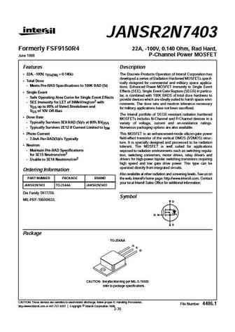
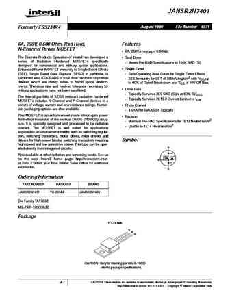
JANSR2N7403 Formerly FSF9150R4 22A, -100V, 0.140 Ohm, Rad Hard, June 1998 P-Channel Power MOSFET Features Description 22A, -100V, rDS(ON) = 0.140 The Discrete Products Operation of Intersil Corporation has developed a series of Radiation Hardened MOSFETs specif- Total Dose ically designed for commercial and military space applica- - Meets Pre-RAD Specifications to 100K RAD (S
jansr2n7406.pdf
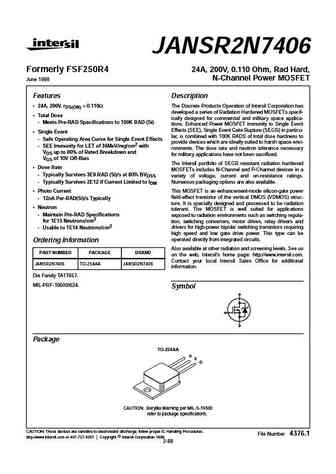
JANSR2N7406 Formerly FSF250R4 24A, 200V, 0.110 Ohm, Rad Hard, June 1998 N-Channel Power MOSFET Features Description 24A, 200V, rDS(ON) = 0.110 The Discrete Products Operation of Intersil Corporation has developed a series of Radiation Hardened MOSFETs specif- Total Dose ically designed for commercial and military space applica- - Meets Pre-RAD Specifications to 100K RAD (Si)
2n7405.pdf
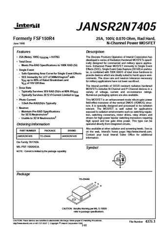
JANSR2N7405 Formerly FSF150R4 25A, 100V, 0.070 Ohm, Rad Hard, June 1998 N-Channel Power MOSFET Features Description 25A (Note), 100V, rDS(ON) = 0.070 The Discrete Products Operation of Intersil Corporation has developed a series of Radiation Hardened MOSFETs specif- Total Dose ically designed for commercial and military space applica- - Meets Pre-RAD Specifications to 100K RA
jansr2n7405.pdf
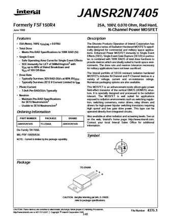
JANSR2N7405 Formerly FSF150R4 25A, 100V, 0.070 Ohm, Rad Hard, June 1998 N-Channel Power MOSFET Features Description 25A (Note), 100V, rDS(ON) = 0.070 The Discrete Products Operation of Intersil Corporation has developed a series of Radiation Hardened MOSFETs specif- Total Dose ically designed for commercial and military space applica- - Meets Pre-RAD Specifications to 100K RA
jansr2n7402.pdf
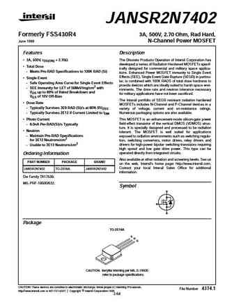
JANSR2N7402 Formerly FSS430R4 3A, 500V, 2.70 Ohm, Rad Hard, June 1998 N-Channel Power MOSFET Features Description 3A, 500V, rDS(ON) = 2.70 The Discrete Products Operation of Intersil Corporation has developed a series of Radiation Hardened MOSFETs specif- Total Dose ically designed for commercial and military space applica- - Meets Pre-RAD Specifications to 100K RAD (Si) tio
jansr2n7404.pdf
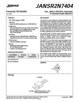
JANSR2N7404 Formerly FSF9250R4 15A, -200V, 0.290 Ohm, Rad Hard, June 1998 P-Channel Power MOSFET Features Description 15A, -200V, rDS(ON) = 0.290 The Discrete Products Operation of Intersil Corporation has developed a series of Radiation Hardened MOSFETs specif- Total Dose ically designed for commercial and military space applica- - Meets Pre-RAD Specifications to 100K RAD (S
jansr2n7400.pdf

JANSR2N7400 Formerly FSS230R4 8A, 200V, 0.440 Ohm, Rad Hard, June 1998 N-Channel Power MOSFET Features Description 8A, 200V, rDS(ON) = 0.440 The Discrete Products Operation of Intersil Corporation has developed a series of Radiation Hardened MOSFETs specif- Total Dose ically designed for commercial and military space applica- - Meets Pre-RAD Specifications to 100K RAD (Si) t
2n3740r.pdf
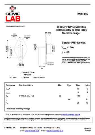
2N3740R Dimensions in mm (inches). Bipolar PNP Device in a Hermetically sealed TO66 6.35 (0.250) Metal Package. 8.64 (0.340) 3.68 (0.145) rad. 3.61 (0.142) max. 4.08(0.161) rad. Bipolar PNP Device. 1 2 VCEO = 60V IC = 4A All Semelab hermetically sealed products can be processed in accordance with the requirements of BS, CECC and JAN, JANTX, JANTXV and JANS speci
2sc1740s.pdf
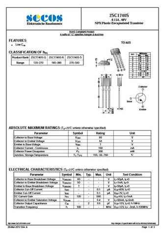
2SC1740S 0.15A , 60V NPN Plastic-Encapsulated Transistor Elektronische Bauelemente RoHS Compliant Product A suffix of -C specifies halogen & lead-free FEATURES TO-92S Low Cob CLASSIFICATION OF hFE Millimeter REF. Min. Max. A 3.90 4.10 Product-Rank 2SC1740S-Q 2SC1740S-R 2SC1740S-S B 3.05 3.25 C 1.42 1.62 Range 120 270 180 390 270 560 D 15.1 15.5 E 2.9
ssf7401.pdf
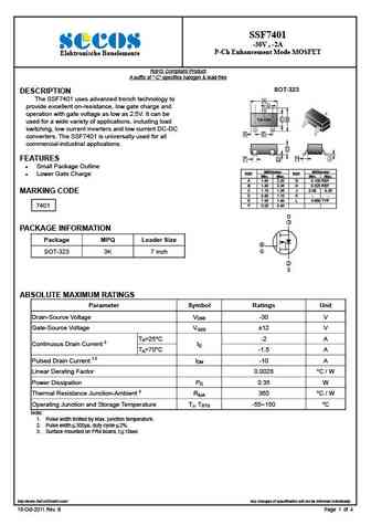
SSF7401 -30V , -2A P-Ch Enhancement Mode MOSFET Elektronische Bauelemente RoHS Compliant Product A suffix of -C specifies halogen & lead-free SOT-323 DESCRIPTION The SSF7401 uses advanced trench technology to A L provide excellent on-resistance, low gate charge and 3 3 operation with gate voltage as low as 2.5V. It can be Top View C B used for a wide variety of
ssf7400.pdf
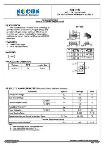
SSF7400 30V , 1.7A , RDS(ON) 85m N-Ch Enhancement Mode Power MOSFET Elektronische Bauelemente RoHS Compliant Product A suffix of -C specifies halogen & lead-free DESCRIPTION SOT-323 The SSF7400 uses advanced trench technology to provide excellent on-resistance, low gate charge and A L operation with gate voltage as low as 2.5V. It can be 3 3 used for a wide va
tsm7401cs.pdf
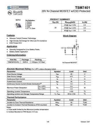
TSM7401 20V N-Channel MOSFET w/ESD Protected PRODUCT SUMMARY SOP-8 Pin Definition 1. Source VDS (V) RDS(on)(m ) ID (A) 2. Source 25 @ VGS = 4.5V 4.5 3. Source 4. Gate 20 30 @ VGS = 2.5V 3.5 5, 6, 7, 8. Drain 65 @ VGS = 1.8V 2.0 Features Block Diagram Advance Trench Process Technology High Density Cell Design for Ultra Low On-resistance ESD P
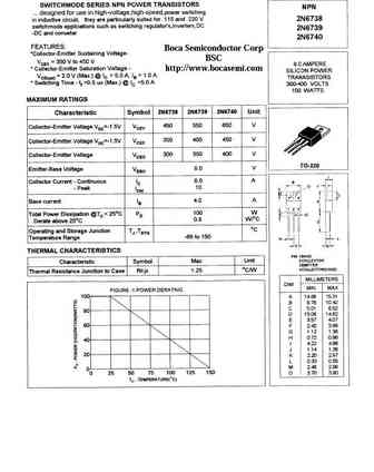
2n6738 2n6739 2n6740.pdf
A Boca Semiconductor Corp BSC http //www.bocasemi.com A Boca Semiconductor Corp BSC http //www.bocasemi.com A Boca Semiconductor Corp BSC http //www.bocasemi.com
csc1740.pdf
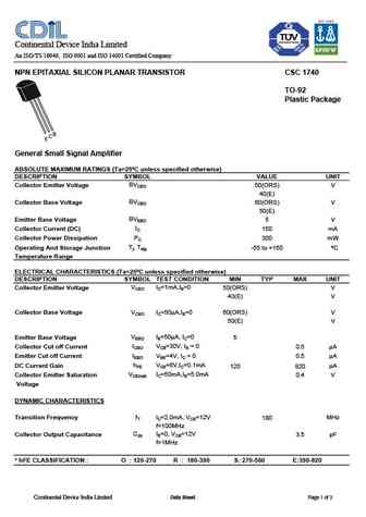
Q Continental Device India Limited An ISO/TS 16949, ISO 9001 and ISO 14001 Certified Company NPN EPITAXIAL SILICON PLANAR TRANSISTOR CSC 1740 TO-92 Plastic Package General Small Signal Amplifier ABSOLUTE MAXIMUM RATINGS (Ta=25 C unless specified otherwise) DESCRIPTION SYMBOL VALUE UNIT BVCEO Collector Emitter Voltage 50(ORS) V 40(E) BVCBO Collector Base Voltage 60(ORS) V 50(E) B
2n6740.pdf
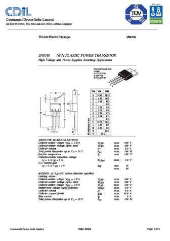
Continental Device India Limited An ISO/TS 16949, ISO 9001 and ISO 14001 Certified Company TO-220 Plastic Package 2N6740 2N6740 NPN PLASTIC POWER TRANSISTOR High Voltage and Power Supplies Switching Applications PIN CONFIGURATION 4 1. BASE 2. COLLECTOR 3. EMITTER 4. COLLECTOR 1 2 3 C DIM MIN. MAX. B E F A 14.42 16.51 B 9.63 10.67 C 3.56 4.83 D0.90 E 1.15 1.40 1 2 3 F 3.75
2sc1740s.pdf
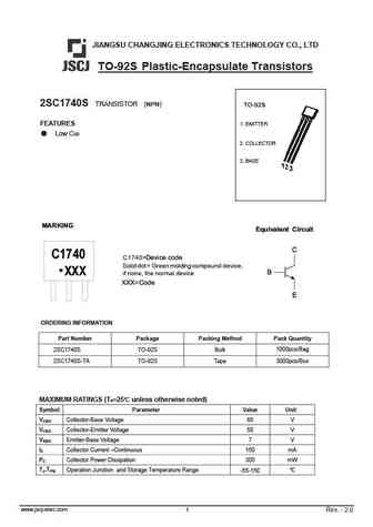
JIANGSU CHANGJING ELECTRONICS TECHNOLOGY CO., LTD TO-92S Plastic-Encapsulate Transistors 2SC1740S TRANSISTOR (NPN) TO-92S FEATURES 1. EMITTER Low Cob 2. COLLECTOR 3. BASE Equivalent Circuit C1740 C1740=Device code Solid dot = Green molding compound device, if none, the normal device XXX=Code ORDERING INFORMATION Part Number Package Packing Method Pack
2sa1740.pdf
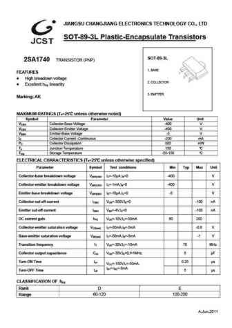
JIANGSU CHANGJIANG ELECTRONICS TECHNOLOGY CO., LTD SOT-89-3L Plastic-Encapsulate Transistors SOT-89-3L 2SA1740 TRANSISTOR (PNP) 1. BASE FEATURES High breadown voltage 2. COLLECTOR Excellent hFE linearlity 3. EMITTER Marking AK MAXIMUM RATINGS (Ta=25 unless otherwise noted) Symbol Parameter Value Unit VCBO Collector-Base Voltage -400 V VCEO Collector-Emitter
2sa740.pdf
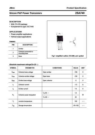
JMnic Product Specification Silicon PNP Power Transistors 2SA740 DESCRIPTION With TO-220 package Complement to type 2SC1448 APPLICATIONS Power amplifier applications Vertical output applications PINNING PIN DESCRIPTION 1 Emitter Collector;connected to 2 mounting base Fig.1 simplified outline (TO-220) and symbol 3 Base Absolute maximum ratings(Ta=25 ) SYM
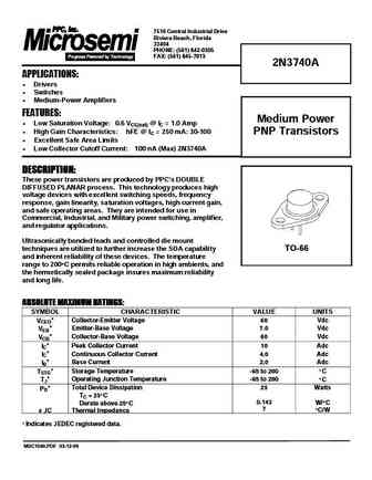
2n3740a.pdf
7516 Central Industrial Drive Riviera Beach, Florida 33404 PHONE (561) 842-0305 FAX (561) 845-7813 2N3740A APPLICATIONS Drivers Switches Medium-Power Amplifiers FEATURES Medium Power Low Saturation Voltage 0.6 VCE(sat) @ IC = 1.0 Amp High Gain Characteristics hFE @ IC = 250 mA 30-100 PNP Transistors Excellent Safe Area Limits Low Collector Cuto
2n3740.pdf
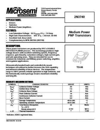
7516 Central Industrial Drive Riviera Beach, Florida 33404 PHONE (561) 842-0305 FAX (561) 845-7813 2N3740 APPLICATIONS Drivers Switches Medium-Power Amplifiers FEATURES Medium Power Low Saturation Voltage 0.6 VCE(sat) @ IC = 1.0 Amp High Gain Characteristics hFE @ IC = 250 mA 30-100 PNP Transistors Excellent Safe Area Limits Complementary to NP
cep740a ceb740a cef740a.pdf
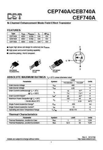
CEP740A/CEB740A CEF740A N-Channel Enhancement Mode Field Effect Transistor FEATURES Type VDSS RDS(ON) ID @VGS CEP740A 400V 0.55 10A 10V CEB740A 400V 0.55 10A 10V CEF740A 400V 0.55 10A d 10V D Super high dense cell design for extremely low RDS(ON). High power and current handing capability. Lead-free plating ; RoHS compliant. G S CEB SERIES CEP SERIES CEF SERIES TO-263(D
cep740g ceb740g cef740g.pdf
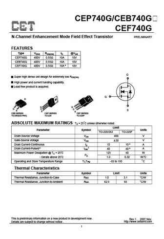
CEP740G/CEB740G CEF740G N-Channel Enhancement Mode Field Effect Transistor PRELIMINARY FEATURES Type VDSS RDS(ON) ID @VGS CEP740G 400V 0.55 10A 10V CEB740G 400V 0.55 10A 10V CEF740G 400V 0.55 10A e 10V D Super high dense cell design for extremely low RDS(ON). High power and current handing capability. Lead free product is acquired. G S CEB SERIES CEP SERIES CEF SERIES T
ceu740a ced740a.pdf
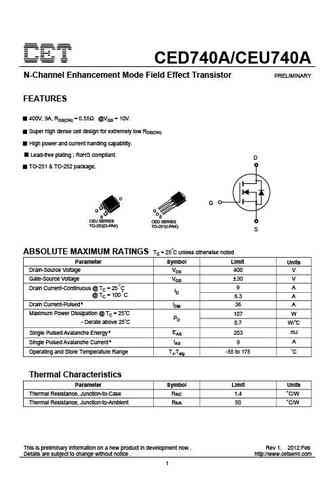
CED740A/CEU740A N-Channel Enhancement Mode Field Effect Transistor PRELIMINARY FEATURES 400V, 9A, RDS(ON) = 0.55 @VGS = 10V. Super high dense cell design for extremely low RDS(ON). High power and current handing capability. Lead-free plating ; RoHS compliant. D TO-251 & TO-252 package. D G G S CEU SERIES CED SERIES TO-252(D-PAK) TO-251(I-PAK) S ABSOLUTE MAXIMUM RATINGS Tc =
2sc1740s to-92s.pdf
2SC1740S TO-92S Transistor (NPN) 1. EMITTER TO-92S 2. COLLECTOR 3. BASE 1 2 3 Features Low Cob MAXIMUM RATINGS (TA=25 unless otherwise noted) Symbol Parameter Value Units VCBO Collector-Base Voltage 60 V VCEO Collector-Emitter Voltage 50 V VEBO Emitter-Base Voltage 7 V IC Collector Current Continuous 150 mA PC Collector Power Dissipation 300 mW TJ Junction Te
2sa1740.pdf
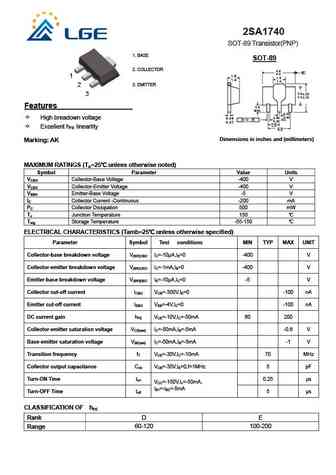
2SA1740 SOT-89 Transistor(PNP) 1. BASE SOT-89 2. COLLECTOR 4.6 B 4.4 1.6 1 1.8 1.4 1.4 3. EMITTER 2 2.6 4.25 3 2.4 3.75 Features 0.8 MIN 0.53 0.40 0.48 High breadown voltage 0.44 2x) 0.13 B 0.35 0.37 1.5 Excellent hFE linearlity 3.0 Dimensions in inches and (millimeters) Marking AK MAXIMUM RATINGS (TA=25 unless otherwise noted) Symbol Param
hirf740.pdf
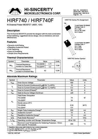
Spec. No. MOS200512 HI-SINCERITY Issued Date 2005.09.01 Revised Date 2005.09.22 MICROELECTRONICS CORP. Page No. 1/4 HIRF740 Series Pin Assignment HIRF740 / HIRF740F Tab N-Channel Power MOSFET (400V, 10A) 3-Lead Plastic TO-220AB Package Code E Pin 1 Gate Pin 2 & Tab Drain Description Pin 3 Source This N-Channel MOSFETs provide the designer with the best combination o
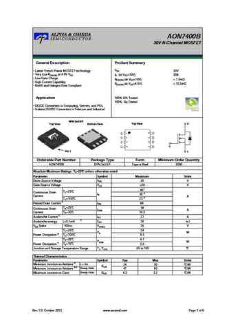
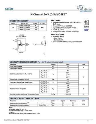
aon7400.pdf

AON7400 30V N-Channel MOSFET General Description Product Summary VDS 30V The AON7400 uses advanced trench technology and design to provide excellent RDS(ON) with low gate charge. ID (at VGS=10V) 26A This device is suitable for use in DC - DC converters and RDS(ON) (at VGS=10V)
aon7405.pdf

AON7405 30V P-Channel MOSFET General Description Product Summary VDS -30V The AON7405 uses advanced trench technology to provide excellent RDS(ON) with low gate charge. ID (at VGS= -10V) -50A This device is ideal for load switch and battery protection RDS(ON) (at VGS= -10V)
ao7401.pdf
AO7401 30V P-Channel MOSFET General Description Product Summary VDS The AO7401 uses advanced trench technology to -30V provide excellent RDS(ON), low gate charge, and ID (at VGS=-10V) -1.4A operation with gate voltages as low as 2.5V, in the RDS(ON) (at VGS=-10V)
aon7402.pdf
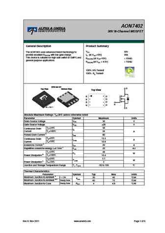
AON7402 30V N-Channel MOSFET General Description Product Summary VDS 30V The AON7402 uses advanced trench technology to provide excellent RDS(ON) with low gate charge. ID (at VGS=10V) 39A This device is suitable for high side switch in SMPS and RDS(ON) (at VGS=10V)
ao7403.pdf
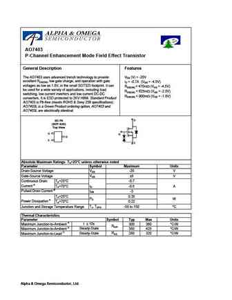
AO7403 P-Channel Enhancement Mode Field Effect Transistor General Description Features The AO7403 uses advanced trench technology to provide VDS (V) = -20V excellent RDS(ON), low gate charge, and operation with gate ID = -0.7A (VGS = -4.5V) voltages as low as 1.8V, in the small SOT323 footprint. It can RDS(ON)
ao7400.pdf
AO7400 30V N-Channel MOSFET General Description Product Summary VDS 30V The AO7400 uses advanced trench technology to provide excellent RDS(ON), low gate charge and ID (at VGS=10V) 1.7A operation with gate voltages as low as 2.5V, in the RDS(ON) (at VGS=10V)
aon7408.pdf

AON7408 30V N-Channel MOSFET General Description Product Summary VDS 30V The AON7408 uses advanced trench technology and design to provide excellent RDS(ON) with low gate charge. ID (at VGS=10V) 18A This device is suitable for use in general purpose RDS(ON) (at VGS=10V)
aon7406.pdf
AON7406 30V N-Channel MOSFET General Description Product Summary VDS 30V The AON7406 uses advanced trench technology and design to provide excellent RDS(ON) with low gate charge. ID (at VGS=10V) 25A This device is suitable for use in SMPS and general RDS(ON) (at VGS=10V)
ao7408.pdf
AO7408 20V N-Channel MOSFET General Description Product Summary VDS 20V The AO7408 uses advanced trench technology to provide excellent RDS(ON), low gate charge and operation with ID (at VGS=10V) 2A gate voltages as low as 1.8V. This device is suitable for RDS(ON) (at VGS=4.5V)
aon7403.pdf

AON7403 30V P-Channel MOSFET General Description Product Summary VDS -30V The AON7403 uses advanced trench technology to provide excellent RDS(ON), and ultra-low low gate charge ID (at VGS=-10V) -29A with a 25V gate rating. This device is suitable for use as a RDS(ON) (at VGS=-10V)
aons77402.pdf
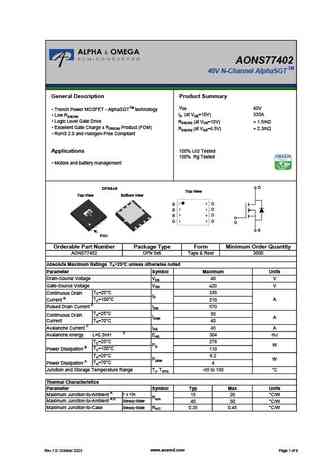
AONS77402 TM 40V N-Channel AlphaSGT General Description Product Summary VDS 40V Trench Power MOSFET - AlphaSGTTM technology ID (at VGS=10V) 335A Low RDS(ON) Logic Level Gate Drive RDS(ON) (at VGS=10V)
ao7405.pdf
AO7405 30V P-Channel MOSFET General Description Product Summary VDS The AO7405 uses advanced trench technology to -30V provide excellent RDS(ON), low gate charge, and ID (at VGS=-10V) -1.4A operation with gate voltages as low as 2.5V, in the RDS(ON) (at VGS=-10V)
ao7404.pdf
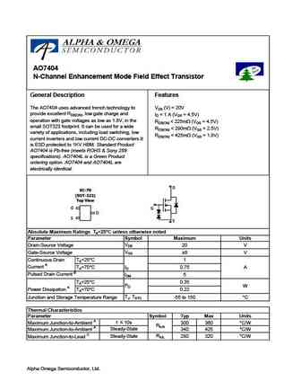
AO7404 N-Channel Enhancement Mode Field Effect Transistor General Description Features The AO7404 uses advanced trench technology to VDS (V) = 20V provide excellent RDS(ON), low gate charge and ID = 1 A (VGS = 4.5V) operation with gate voltages as low as 1.8V, in the RDS(ON)
aon7400b.pdf
AON7400B 30V N-Channel MOSFET General Description Product Summary VDS Latest Trench Power MOSFET technology 30V Very Low RDS(ON) at 4.5V VGS ID (at VGS=10V) 30A Low Gate Charge RDS(ON) (at VGS=10V)
aon7409.pdf

AON7409 30V P-Channel MOSFET General Description Product Summary VDS The AON7409 combines advanced trench MOSFET -30V technology with a low resistance package to provide ID (at VGS=-10V) -32A extremely low RDS(ON). This device is ideal for load switch RDS(ON) (at VGS=-10V)
aon7401.pdf
AON7401 30V P-Channel MOSFET General Description Product Summary VDS -30V The AON7401 uses advanced trench technology to provide excellent RDS(ON), and ultra-low low gate charge ID (at VGS=-10V) -35A with a 25V gate rating. This device is suitable for use as a RDS(ON) (at VGS=-10V)
ao7407.pdf
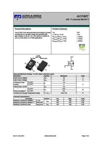
AO7407 20V P-Channel MOSFET General Description Product Summary VDS -20V The AO7407 uses advanced trench technology to provide excellent RDS(ON), low gate charge and operation with ID (at VGS=-4.5V) -1.2A gate voltages as low as 1.8V. This device is suitable for RDS(ON) (at VGS=-4.5V)
aon7404g.pdf
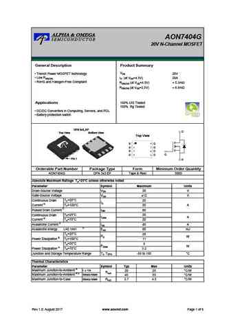
AON7404G 20V N-Channel MOSFET General Description Product Summary VDS Trench Power MOSFET technology 20V Low RDS(ON) ID (at VGS=4.5V) 20A RoHS and Halogen-Free Compliant RDS(ON) (at VGS=4.5V)
aon7407.pdf
AON7407 20V P-Channel MOSFET General Description Product Summary VDS -20V The AON7407 combines advanced trench MOSFET technology with a low resistance package to provide ID (at VGS=-4.5V) -40A extremely low RDS(ON). This device is ideal for load switch RDS(ON) (at VGS =-4.5V)
aon7404.pdf
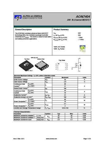
AON7404 20V N-Channel MOSFET General Description Product Summary VDS 20V The AON7404 combines advanced trench MOSFET technology with a low resistance package to provide ID (at VGS=4.5V) 20A extremely low RDS(ON). This device is ideal for load switch RDS(ON) (at VGS=4.5V)
am7401p.pdf

Analog Power AM7401P P-Channel 150-V (D-S) MOSFET PRODUCT SUMMARY Key Features rDS(on) (m ) VDS (V) ID(A) Low r trench technology DS(on) 140 @ VGS = -10V -4.9 Low thermal impedance -150 150 @ VGS = -5.5V -4.8 Fast switching speed Typical Applications DFN5X6-8L White LED boost converters Automotive Systems Industrial DC/DC Conversion Circuits
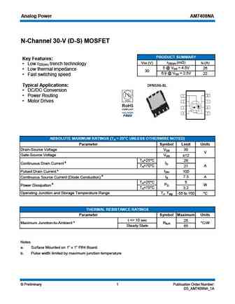
am7406na.pdf
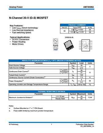
Analog Power AM7406NA N-Channel 30-V (D-S) MOSFET PRODUCT SUMMARY Key Features rDS(on) (m ) VDS (V) ID (A) Low r trench technology DS(on) 3 @ VGS = 4.5V 34 Low thermal impedance 30 4.2 @ VGS = 2.5V 29 Fast switching speed Typical Applications DFN5X6-8L DC/DC Conversion Power Routing Motor Drives ABSOLUTE MAXIMUM RATINGS (TA = 25 C UNLESS
am7402n.pdf
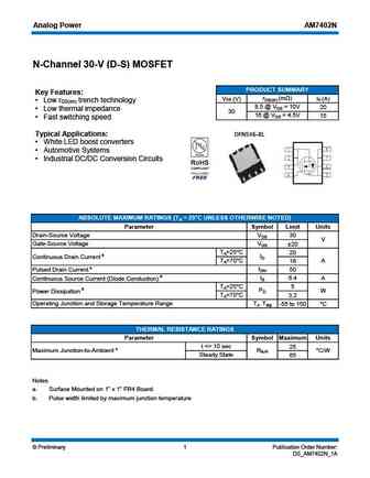
Analog Power AM7402N N-Channel 30-V (D-S) MOSFET PRODUCT SUMMARY Key Features rDS(on) (m ) VDS (V) ID (A) Low r trench technology DS(on) 8.5 @ VGS = 10V 20 Low thermal impedance 30 16 @ VGS = 4.5V 15 Fast switching speed Typical Applications DFN5X6-8L White LED boost converters Automotive Systems Industrial DC/DC Conversion Circuits ABSOLU
am7408na.pdf
Analog Power AM7408NA N-Channel 30-V (D-S) MOSFET PRODUCT SUMMARY Key Features rDS(on) (m ) VDS (V) ID (A) Low r trench technology DS(on) 5 @ VGS = 4.5V 26 Low thermal impedance 30 6.9 @ VGS = 2.5V 22 Fast switching speed Typical Applications DFN5X6-8L DC/DC Conversion Power Routing Motor Drives ABSOLUTE MAXIMUM RATINGS (TA = 25 C UNLESS
am7404na.pdf

Analog Power AM7404NA N-Channel 30-V (D-S) MOSFET PRODUCT SUMMARY Key Features rDS(on) (m ) VDS (V) ID (A) Low r trench technology DS(on) 2.8 @ VGS = 10V 35 Low thermal impedance 30 4 @ VGS = 4.5V 29 Fast switching speed Typical Applications DFN5X6-8L Synchronous Buck DC/DC Conversion Synchronous Rectification Power Routing and ORing ABSOL
am7403p.pdf
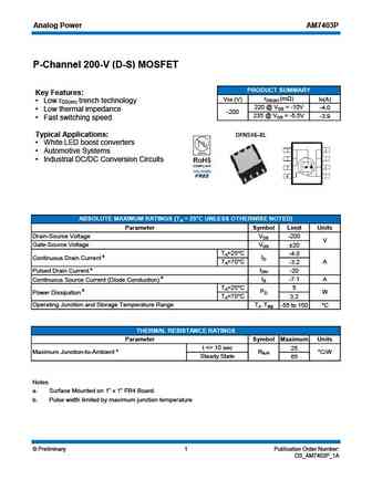
Analog Power AM7403P P-Channel 200-V (D-S) MOSFET PRODUCT SUMMARY Key Features rDS(on) (m ) VDS (V) ID(A) Low r trench technology DS(on) 220 @ VGS = -10V -4.0 Low thermal impedance -200 235 @ VGS = -5.5V -3.9 Fast switching speed Typical Applications DFN5X6-8L White LED boost converters Automotive Systems Industrial DC/DC Conversion Circuits
am7400n.pdf

Analog Power AM7400N N-Channel 30-V (D-S) MOSFET PRODUCT SUMMARY Key Features rDS(on) (m ) VDS (V) ID(A) Low r trench technology DS(on) 2.5 @ VGS = 10V 36.6 Low thermal impedance 30 4 @ VGS = 4.5V 28.9 Fast switching speed DFN5X6-8L Typical Applications White LED boost converters Automotive Systems Industrial DC/DC Conversion Circuits ABSO
afn7402.pdf
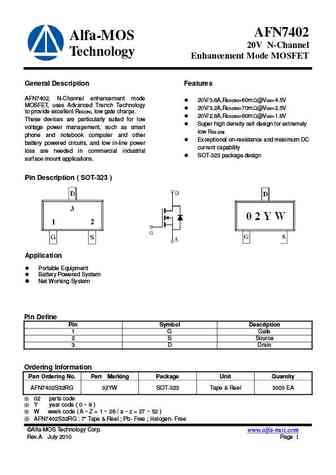
AFN7402 Alfa-MOS 20V N-Channel Technology Enhancement Mode MOSFET General Description Features AFN7402, N-Channel enhancement mode 20V/3.6A,RDS(ON)=60m @VGS=4.5V MOSFET, uses Advanced Trench Technology 20V/3.2A,RDS(ON)=70m @VGS=2.5V to provide excellent RDS(ON), low gate charge. 20V/2.8A,RDS(ON)=90m @VGS=1.8V These devices are particularly suited for low Supe
afn7400.pdf

AFN7400 Alfa-MOS 30V N-Channel Technology Enhancement Mode MOSFET General Description Features AFN7400, N-Channel enhancement mode 30V/3.6A,RDS(ON)=82m @VGS=10V MOSFET, uses Advanced Trench Technology 30V/3.0A,RDS(ON)=90m @VGS=4.5V to provide excellent RDS(ON), low gate charge. 30V/2.2A,RDS(ON)=102m @VGS=2.5V These devices are particularly suited for low Supe
irfs740.pdf
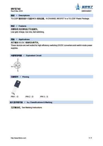
IRFS740 Rev.D Mar.-2016 DATA SHEET / Descriptions TO-220F N MOS N-CHANNEL MOSFET in a TO-220F Plastic Package. / Features , , Low gate charge, low crss, fast switching. / Applications DC/DC These devices are well suited for high efficiency
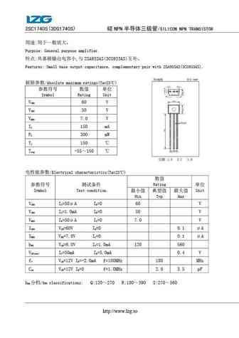
2sc1740m.pdf
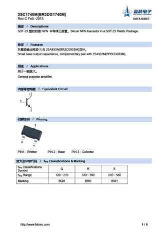
2SC1740M(BR3DG1740M) Rev.C Feb.-2015 DATA SHEET / Descriptions SOT-23 NPN Silicon NPN transistor in a SOT-23 Plastic Package. / Features , 2SA933M(BR3CG933M) Small base output capacitance, complementary pair with 2SA933M(BR3CG933M). / Applications General purpose a
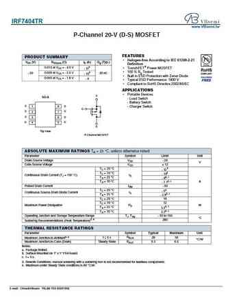
irf740.pdf
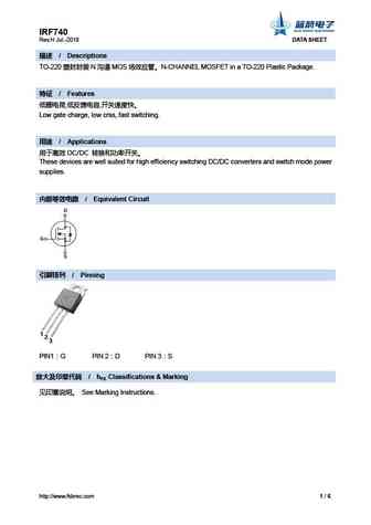
IRF740 Rev.H Jul.-2018 DATA SHEET / Descriptions TO-220 N MOS N-CHANNEL MOSFET in a TO-220 Plastic Package. / Features , , Low gate charge, low crss, fast switching. / Applications DC/DC These devices are well suited for high efficiency swi
bri740.pdf
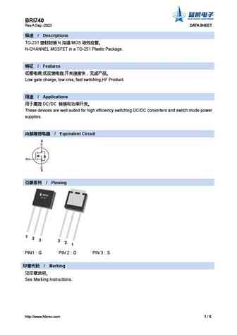
BRI740 Rev.A Sep.-2023 DATA SHEET / Descriptions TO-251 N MOS N-CHANNEL MOSFET in a TO-251 Plastic Package. / Features , , Low gate charge, low crss, fast switching,HF Product. / Applications DC/DC These devices are well su
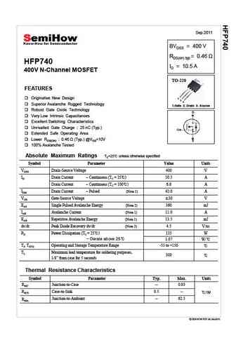
hfp740.pdf
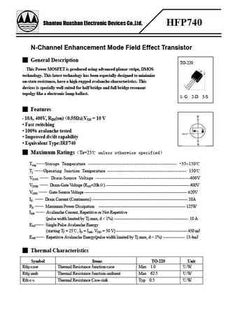
Shantou Huashan Electronic Devices Co.,Ltd. HFP740 N-Channel Enhancement Mode Field Effect Transistor General Description TO-220 This Power MOSFET is produced using advanced planar stripe, DMOS technology. This latest technology has been especially designed to minimize on-state resistance, have a high rugged avalanche characteristics. This devices is specially well suited f
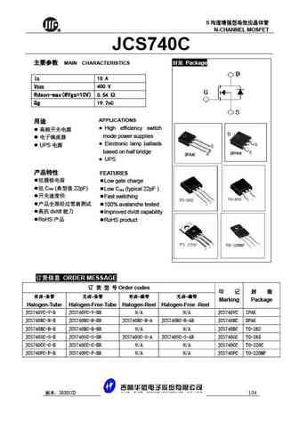
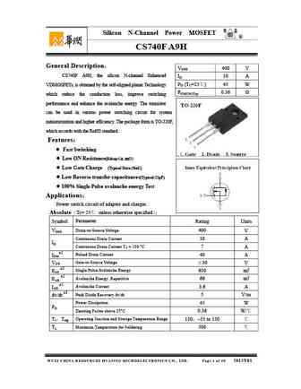
cs740f a9h.pdf

Silicon N-Channel Power MOSFET R CS740F A9H General Description VDSS 400 V CS740F A9H, the silicon N-channel Enhanced ID 10 A PD (TC=25 ) 45 W VDMOSFETs, is obtained by the self-aligned planar Technology RDS(ON)Typ 0.36 which reduce the conduction loss, improve switching performance and enhance the avalanche energy. The transistor can be used in various pow
cs740 a0h.pdf
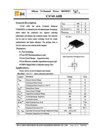
Silicon N-Channel Power MOSFET R CS740 A0H General Description VDSS 400 V CS740 A0H, the silicon N-channel Enhanced ID 10 A PD (TC=25 ) 120 W VDMOSFETs, is obtained by the self-aligned planar Technology RDS(ON)Typ 0.36 which reduce the conduction loss, improve switching performance and enhance the avalanche energy. The transistor can be used in various power
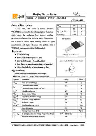
cs740 a8h.pdf
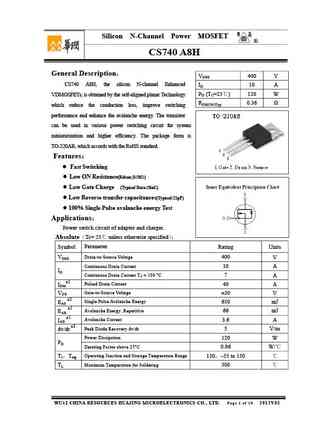
Silicon N-Channel Power MOSFET R CS740 A8H General Description VDSS 400 V CS740 A8H, the silicon N-channel Enhanced ID 10 A PD (TC=25 ) 120 W VDMOSFETs, is obtained by the self-aligned planar Technology RDS(ON)Typ 0.36 which reduce the conduction loss, improve switching performance and enhance the avalanche energy. The transistor can be used in various power
krf7401.pdf
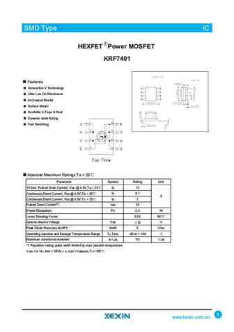
SMD Type IC SMD Type IC HEXFET Power MOSFET KRF7401 Features Generation V Technology Ultra Low On-Resistance N-Channel Mosfet Surface Mount Available in Tape & Reel Dynamic dv/dt Rating Fast Switching Absolute Maximum Ratings Ta = 25 Parameter Symbol Rating Unit 10 Sec. Pulsed Drain Current, VGS @4.5V,Ta =25 ID 10 Continuous Drain Current, VGS @4.5V,Ta =25 ID 8.7 A Continuous D
ao7400.pdf
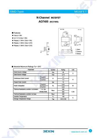
SMD Type MOSFET N-Channel MOSFET AO7400 (KO7400) Features VDS (V) = 30V ID = 1.7 A (VGS = 10V) RDS(ON) 55m (VGS = 10V) D RDS(ON) 65m (VGS = 4.5V) RDS(ON) 85m (VGS = 2.5V) 1 Gate 2 Source G 3 Drain S Absolute Maximum Ratings Ta = 25 Parameter Symbol Rating Unit Drain-Source Voltage VDS 30 V Gate-Source Voltage VGS 12
bfp740.pdf
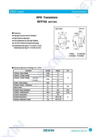
SMD Type Transistors NPN Transistors BFP740 (KFP740) Uint mm SOT-343 0.9 0.1 0.2 2 Features 0.1 MAX. 1.3 0.1 High gain ultra low noise RF transistor A 4 3 High maximum stable gain Gold metallization for extra high reliability 0.15 150 GHz fT-Silicon Germanium technology 1 2 +0.1 +0.1 Outstanding noise figure F = 0.5 dB at 1.8 GHz 0.3 0.15
2sa1740.pdf
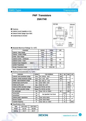
SMD Type Transistors PNP Transistors 2SA1740 SOT-89 Unit mm 1.70 0.1 Features Collector Current Capability IC=-0.2A Collector Emitter Voltage VCEO=-400V Complementary to 2SC4548 0.42 0.1 0.46 0.1 1.Base 2.Collector 3.Emitter Absolute Maximum Ratings Ta = 25 Parameter Symbol Rating Unit Collector - Base Voltage VCBO -400 Collector - Emitter Voltage V
sff740.pdf
SFF740 SFF740 SFF740 SFF740 Silicon N-Channel MOSFET Silicon N-Channel MOSFET Silicon N-Channel MOSFET Silicon N-Channel MOSFET Features 10A,400V,R (Max 0.55 )@V =10V DS(on) GS Ultra-low Gate Charge(Typical 60nC) Fast Switching Capability 100%Avalanche Tested Maximum Junction Temperature Range(150 ) General Description This Power MOSFET is produced using
sfp740.pdf
SFP740 SFP740 SFP740 SFP740 Silicon N-Channel MOSFET Silicon N-Channel MOSFET Silicon N-Channel MOSFET Silicon N-Channel MOSFET Features 10A,400V,R (Max 0.55 )@V =10V DS(on) GS Ultra-low Gate Charge(Typical 45nC) Fast Switching Capability 100%Avalanche Tested Maximum Junction Temperature Range(150 ) General Description This Power MOSFET is produced using
wff740.pdf
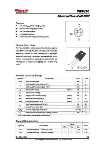
WFF740 WFF740 WFF740 WFF740 Silicon N-Channel MOSFET Silicon N-Channel MOSFET Silicon N-Channel MOSFET Silicon N-Channel MOSFET Features 10A,400V,R (Max 0.55 )@V =10V DS(on) GS Ultra-low Gate Charge(Typical 60nC) Fast Switching Capability 100%Avalanche Tested Maximum Junction Temperature Range(150 ) General Description This Power MOSFET is produced using
wfp740.pdf
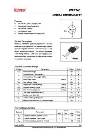
WFP740 WFP740 WFP740 WFP740 Silicon N-Channel MOSFET Silicon N-Channel MOSFET Silicon N-Channel MOSFET Silicon N-Channel MOSFET Features 10A,400V,R (Max 0.55 )@V =10V DS(on) GS Ultra-low Gate Charge(Typical 60nC) Fast Switching Capability 100%Avalanche Tested Maximum Junction Temperature Range(150 ) General Description This Power MOSFET is produced using
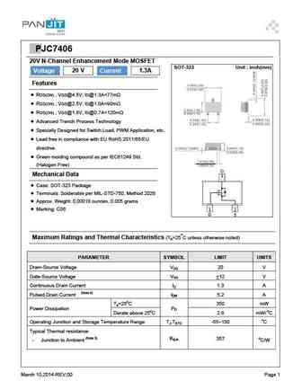
pjc7406.pdf
PPJC7406 20V N-Channel Enhancement Mode MOSFET SOT-323 Unit inch(mm) 20 V 1.3A Voltage Current Features RDS(ON) , VGS@4.5V, ID@1.3A
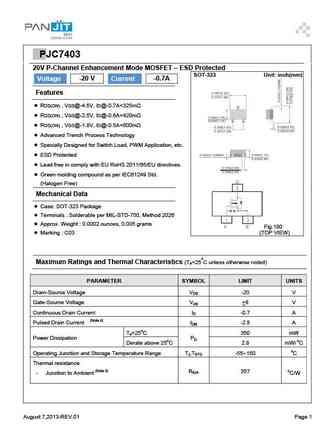
pjc7404.pdf
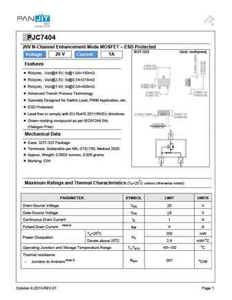
PPJC7404 20V N-Channel Enhancement Mode MOSFET ESD Protected SOT-323 Unit inch(mm) 20 V 1A Voltage Current Features RDS(ON) , VGS@4.5V, ID@1.0A
pjc7401.pdf
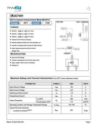
PPJC7401 30V P-Channel Enhancement Mode MOSFET SOT-323 Unit inch(mm) Voltage -30 V Current -1.5A Features RDS(ON) , VGS@-10V, ID@-1.5A
pjt7408.pdf
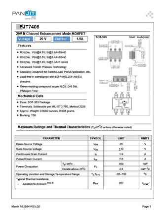
PPJT7408 20V N-Channel Enhancement Mode MOSFET SOT-363 Unit inch(mm) 20 V 1.9A Voltage Current Features RDS(ON) , VGS@4.5V, ID@1.9A
pjc7400.pdf

PPJC7400 30V N-Channel Enhancement Mode MOSFET SOT-323 Unit inch(mm) 30 V 1.9A Voltage Current Features RDS(ON) , VGS@10V, ID@1.9A
pjc7407.pdf
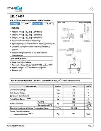
PPJC7407 20V P-Channel Enhancement Mode MOSFET SOT-323 Unit inch(mm) Voltage -20 V Current -1.3A Features RDS(ON) , VGS@-4.5V, ID@-1.3A
am7408.pdf
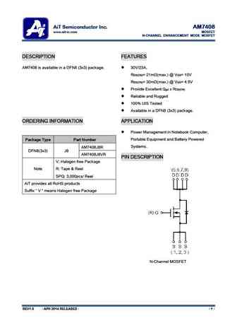
AiT Semiconductor Inc. AM7408 www.ait-ic.com MOSFET N-CHANNEL ENHANCEMENT MODE MOSFET DESCRIPTION FEATURES AM7408 is available in a DFN8 (3x3) package. 30V/23A, R = 21m (max.) @ V = 10V DS(ON) GS R = 30m (max.) @ V = 4.5V DS(ON) GS Provide Excellent Q x R gd DS(ON) Reliable and Rugged 100% UIS Tested Available in a DFN8 (3x3) package. ORDERING INFO
blv740.pdf
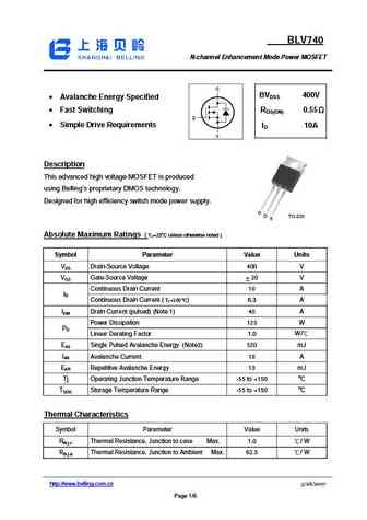
BLV740 N-channel Enhancement Mode Power MOSFET 400V DSS Avalanche Energy Specified BV Fast Switching RDS(ON) 0.55 Simple Drive Requirements ID 10A Description This advanced high voltage MOSFET is produced using Belling s proprietary DMOS technology. Designed for high efficiency switch mode power supply. Absolute Maximum Ratings ( TC=25oC unles
chm7402wgp.pdf
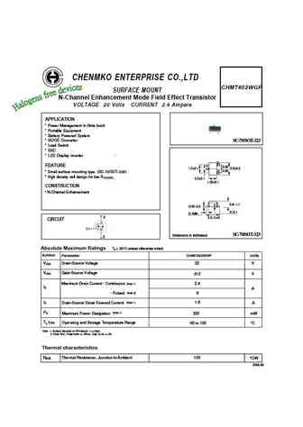
CHENMKO ENTERPRISE CO.,LTD CHM7402WGP SURFACE MOUNT N-Channel Enhancement Mode Field Effect Transistor VOLTAGE 20 Volts CURRENT 2.4 Ampere APPLICATION * Power Management in Note book * Portable Equipment * Battery Powered System * DC/DC Converter SC-70/SOT-323 * Load Switch * DSC . * LCD Display inverter FEATURE 0.65 1.3 0.1 2.0 0.2 0.65 * Small surface mounting type.
chm7401wgp.pdf
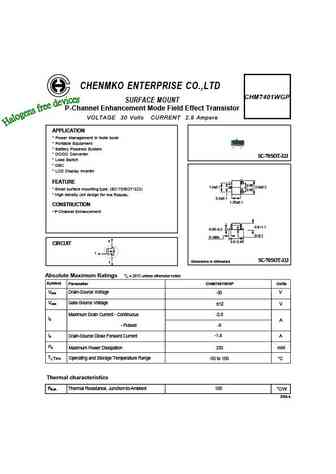
CHENMKO ENTERPRISE CO.,LTD CHM7401WGP SURFACE MOUNT P-Channel Enhancement Mode Field Effect Transistor VOLTAGE 30 Volts CURRENT 2.8 Ampere APPLICATION * Power Management in Note book * Portable Equipment * Battery Powered System * DC/DC Converter SC-70/SOT-323 * Load Switch * DSC * LCD Display inverter FEATURE 0.65 1.3 0.1 2.0 0.2 * Small surface mounting type. (SC-70/S
chm740angp.pdf
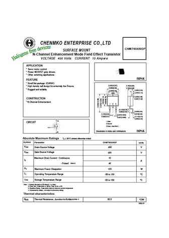
CHENMKO ENTERPRISE CO.,LTD CHM740ANGP SURFACE MOUNT N-Channel Enhancement Mode Field Effect Transistor VOLTAGE 400 Volts CURRENT 10 Ampere APPLICATION * Servo motor control. * Power MOSFET gate drivers. * Other switching applications. D2PAK FEATURE * Small flat package. (D2PAK) 0.420(10.67) 0.190(4.83) * High density cell design for extremely low RDS(ON). 0.380(9.69) 0.160(4
chm7400sgp.pdf
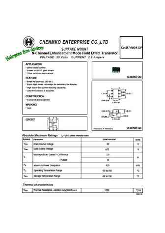
CHENMKO ENTERPRISE CO.,LTD CHM7400SGP SURFACE MOUNT N-Channel Enhancement Mode Field Effect Transistor VOLTAGE 30 Volts CURRENT 2.8 Ampere APPLICATION * Servo motor control. * Power MOSFET gate drivers. * Other switching applications. SC-88/SOT-363 FEATURE * Small flat package. (SC-88 ) * Super high dense cell design for extremely low RDS(ON). * High power and current handing c
chm7407wgp.pdf
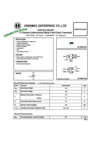
CHENMKO ENTERPRISE CO.,LTD CHM7407WGP SURFACE MOUNT P-Channel Enhancement Mode Field Effect Transistor VOLTAGE 20 Volts CURRENT 2.3 Ampere APPLICATION * Power Management in Note book * Portable Equipment * Battery Powered System * DC/DC Converter SC-70/SOT-323 * Load Switch * DSC * LCD Display inverter FEATURE 0.65 1.3 0.1 2.0 0.2 * Small surface mounting type. (SC-70/S
chm7400wgp.pdf
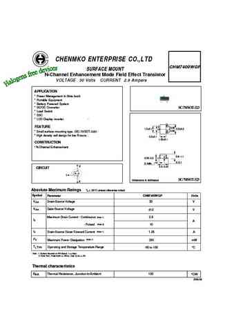
CHENMKO ENTERPRISE CO.,LTD CHM7400WGP SURFACE MOUNT N-Channel Enhancement Mode Field Effect Transistor VOLTAGE 30 Volts CURRENT 2.8 Ampere APPLICATION * Power Management in Note book * Portable Equipment * Battery Powered System * DC/DC Converter SC-70/SOT-323 * Load Switch * DSC . * LCD Display inverter FEATURE 0.65 1.3 0.1 2.0 0.2 0.65 * Small surface mounting type.
elm17400fa.pdf
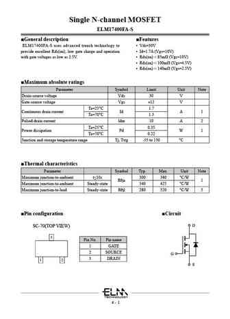
Single N-channel MOSFET ELM17400FA-S General description Features ELM17400FA-S uses advanced trench technology to Vds=30V provide excellent Rds(on), low gate charge and operation Id=1.7A (Vgs=10V) with gate voltages as low as 2.5V. Rds(on)
elm17401fa.pdf
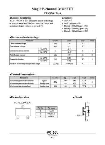
Single P-channel MOSFET ELM17401FA-S General description Features ELM17401FA-S uses advanced trench technology Vds=-30V to provide excellent Rds(on), low gate charge and Id=-1.2A (Vgs=-10V) operation with gate voltages as low as 2.5V. Rds(on)
elm17408ga.pdf
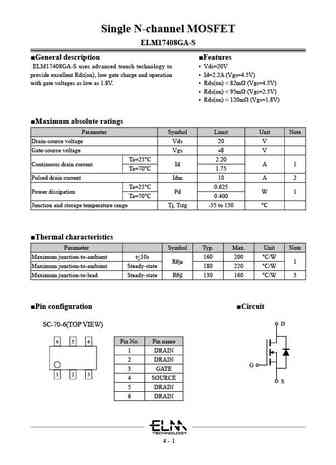
Single N-channel MOSFET ELM17408GA-S General description Features ELM17408GA-S uses advanced trench technology to Vds=20V provide excellent Rds(on), low gate charge and operation Id=2.2A (Vgs=4.5V) with gate voltages as low as 1.8V. Rds(on)
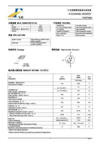
fhp740c.pdf
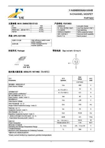
N N-CHANNEL MOSFET FHP740C MAIN CHARACTERISTICS FEATURES ID 10A Low gate charge VDSS 400V Crss ( 2.8pF) Low Crss (typical 2.8pF ) Rdson-typ @Vgs=10V 0.53 Fast switching Qg-typ 15.7nC 100% 100% avalanche tested dv/dt Improved dv
fhp740a.pdf
N N-CHANNEL MOSFET FHP740A MAIN CHARACTERISTICS FEATURES ID 11A Low gate charge VDSS 400V Crss ( 2.8pF) Low Crss (typical 2.8pF ) Rdson-typ @Vgs=10V 0.53 Fast switching Qg-typ 15.7nC 100% 100% avalanche tested dv/dt Improved dv
3dg1740m.pdf
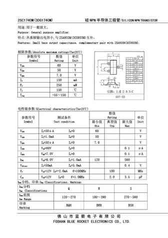
2SC1740M(3DG1740M) NPN /SILICON NPN TRANSISTOR Purpose General purpose amplifier. , 2SA933M(3CG933M) Features Small base output capacitance, complementary pair with 2SA933M(3CG933M). /Absolute maximum ratings(Ta=25 ) Symbol Rating Unit V 60 V
gsm7402.pdf
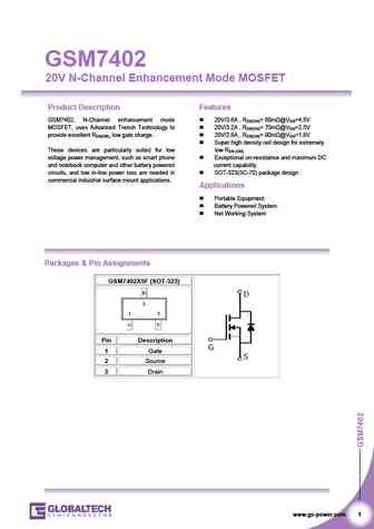
GSM7402 20V N-Channel Enhancement Mode MOSFET Product Description Features GSM7402, N-Channel enhancement mode 20V/3.6A , RDS(ON)= 60m @VGS=4.5V MOSFET, uses Advanced Trench Technology to 20V/3.2A , RDS(ON)= 70m @VGS=2.5V provide excellent RDS(ON), low gate charge. 20V/2.8A , RDS(ON)= 90m @VGS=1.8V Super high density cell design for extremely These devices a
gsm7400.pdf

GSM7400 30V N-Channel Enhancement Mode MOSFET Product Description Features GSM7400, N-Channel enhancement mode 30V/3.6A , RDS(ON)= 82m @VGS=10V MOSFET, uses Advanced Trench Technology to 30V/3.0A , RDS(ON)= 90m @VGS=4.5V provide excellent RDS(ON), low gate charge. 30V/2.2A , RDS(ON)= 102m @VGS=2.5V Super high density cell design for extremely These devices a
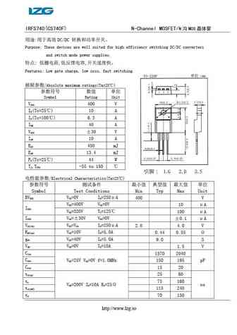
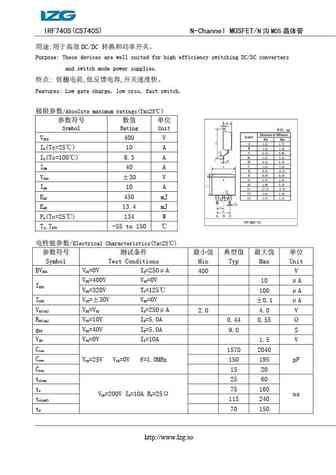
cs740.pdf
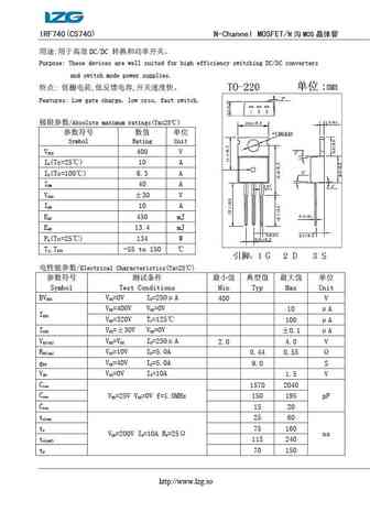
IRF740(CS740) N-Channel MOSFET/N MOS DC/DC Purpose These devices are well suited for high efficiency switching DC/DC converters and switch mode power supplies. , , Features Low gate charge, low crss, fast switch. /Absolute maximum ratings(Ta=25 )
3dg1740s.pdf
2SC1740S(3DG1740S) NPN /SILICON NPN TRANSISTOR Purpose General purpose amplifier. , 2SA933AS(3CG933AS) Features Small base output capacitance, complementary pair with 2SA933AS(3CG933AS). /Absolute maximum ratings(Ta=25 ) Symbol Rating Unit V 60
slp740uz slf740uz.pdf
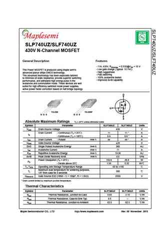
LEAD FREE Pb RoHS SLP740UZ/SLF740UZ SLP740UZ/SLF740UZ 430V N-Channel MOSFET General Description Features - 11A, 430V, RDS(on)typ. = 0.53 @VGS = 10 V - Low gate charge ( typical 15.7nC) This Power MOSFET is produced using Maple semi s - High ruggedness advanced planar stripe DMOS technology. - Fast switching Fast switching This advanced technology has been especially tailored
sld740uz.pdf
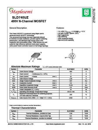
LEAD FREE Pb RoHS SLD740UZ 400V N-Channel MOSFET General Description Features - 11A, 400V, RDS(on)typ. = 0.55 @VGS = 10 V - Low gate charge ( typical 23nC) This Power MOSFET is produced using Maple semi s - High ruggedness advanced trench MOSFET technology. - Fast switching This advanced technology has been especially tailored - 100% avalanche tested to minimize on-sta
mmp7401.pdf
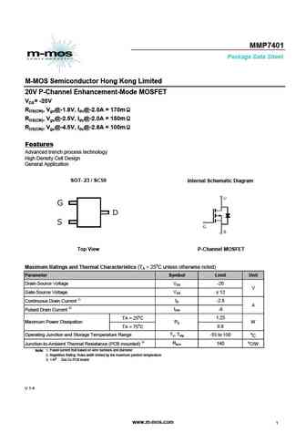
MMP7401 Package Data Sheet M-MOS Semiconductor Hong Kong Limited 20V P-Channel Enhancement-Mode MOSFET VDS= -20V RDS(ON), Vgs@-1.8V, Ids@-2.0A = 170m RDS(ON), Vgs@-2.5V, Ids@-2.0A = 150m RDS(ON), Vgs@-4.5V, Ids@-2.8A = 100m Features Advanced trench process technology High Density Cell Design General Application SOT- 23 / SC59 Internal Schematic Diagram Top View P-Channel M
mmn7402.pdf
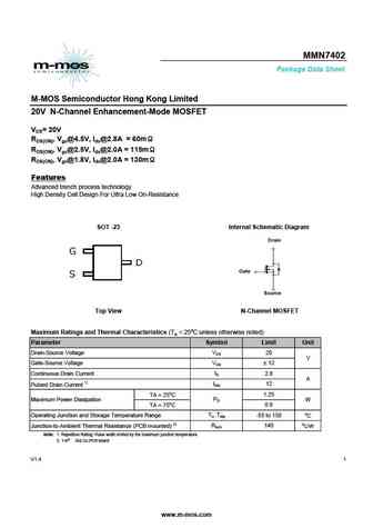
MMN7402 Package Data Sheet M-MOS Semiconductor Hong Kong Limited 20V N-Channel Enhancement-Mode MOSFET VDS= 20V RDS(ON), Vgs@4.5V, Ids@2.8A = 60m RDS(ON), Vgs@2.5V, Ids@2.0A = 115m RDS(ON), Vgs@1.8V, Ids@2.0A = 130m Features Advanced trench process technology High Density Cell Design For Ultra Low On-Resistance SOT -23 Internal Schematic Diagram Drain Gate Source Top
swp740d swf740d.pdf
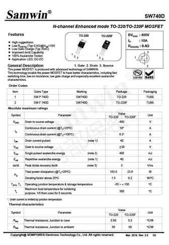
SW740D N-channel Enhanced mode TO-220/TO-220F MOSFET Features BVDSS 400V TO-220 TO-220F ID 10A High ruggedness Low RDS(ON) (Typ 0.4 )@VGS=10V RDS(ON) 0.4 Low Gate Charge (Typ 35nC) 2 Improved dv/dt Capability 1 1 100% Avalanche Tested 2 1 2 3 Application LED, DC-DC 3 1. Gate 2. Drain 3. Source General Description
swp740d swf740d swd740d.pdf
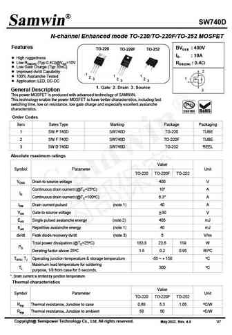
SW740D N-channel Enhanced mode TO-220/TO-220F/TO-252 MOSFET Features BVDSS 400V TO-220 TO-220F TO-252 ID 10A High ruggedness Low RDS(ON) (Typ 0.4 )@VGS=10V RDS(ON) 0.4 Low Gate Charge (Typ 35nC) 2 Improved dv/dt Capability 1 1 1 100% Avalanche Tested 2 1 2 2 3 Application LED, DC-DC 3 3 1. Gate 2. Drain 3. Source General Description 3
hfp740.pdf
Sep 2011 BVDSS = 400 V RDS(on) typ HFP740 ID = 10.5 A 400V N-Channel MOSFET TO-220 FEATURES Originative New Design 1 2 3 Superior Avalanche Rugged Technology 1.Gate 2. Drain 3. Source Robust Gate Oxide Technology Very Low Intrinsic Capacitances Excellent Switching Characteristics Unrivalled Gate Charge 25 nC (Typ.) Extended Safe Operating Area Lowe
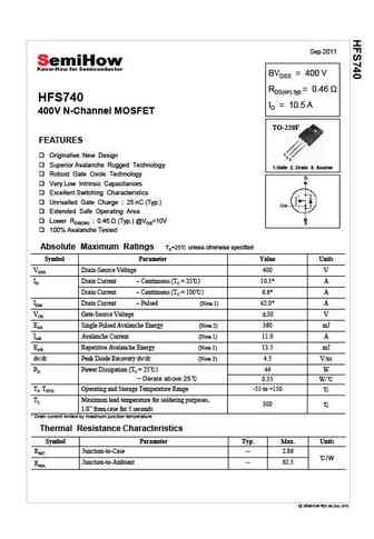
hfs740.pdf
Sep 2011 BVDSS = 400 V RDS(on) typ HFS740 ID = 10.5 A 400V N-Channel MOSFET TO-220F FEATURES 1 Originative New Design 2 3 Superior Avalanche Rugged Technology 1.Gate 2. Drain 3. Source Robust Gate Oxide Technology Very Low Intrinsic Capacitances Excellent Switching Characteristics Unrivalled Gate Charge 25 nC (Typ.) Extended Safe Operating Area Lo
stp7407.pdf
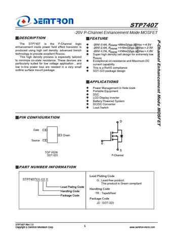
STP7407 -20V P-Channel Enhancement Mode MOSFET DESCRIPTION FEATURE The STP7407 is the P-Channel logic -20V/-3.4A, RDS(ON) =88m (typ.)@VGS =-4.5V enhancement mode power field effect transistor is -20V/-2.4A, RDS(ON) =110m (typ.)@VGS =-2.5V produced using high cell density. advanced trench -20V/-1.7A, RDS(ON) =150m (typ.)@VGS =-1.8V technology to provide excellen
stn7400.pdf
ST7400 N Channel Enhancement Mode MOSFET 2.8A DESCRIPTION ST7400 is the N-Channel logic enhancement mode power field effect transistor which is produced using high cell density, DMOS trench technology. This high density process is especially tailored to minimize on-state resistance. These devices are particularly suited for low voltage application such as cellular phone and noteb
stp7401.pdf
STP7401 P Channel Enhancement Mode MOSFET -2.8A DESCRIPTION STP7401 is the P-Channel logic enhancement mode power field effect transistor which is produced using high cell density, DMOS trench technology. This high density process is especially tailored to minimize on-state resistance. These devices are particularly suited for low voltage application such as cellular phone and not
2sc1740s.pdf
SUNROC 2SC1740S TRANSISTOR (NPN) TO-92S FEATURES 1. EMITTER Low Cob 2. COLLECTOR MAXIMUM RATINGS (TA=25 unless otherwise noted) Symbol Parameter Value Units 3. BASE VCBO Collector-Base Voltage 60 V VCEO Collector-Emitter Voltage 50 V 1 2 3 VEBO Emitter-Base Voltage 7 V IC Collector Current Continuous 150 mA PC Collector Power Dissipation 300 mW TJ Junction
tsp740mr tsf740mr.pdf
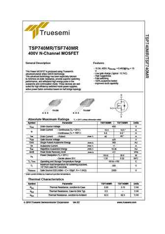
TSP740MR/TSF740MR 400V N-Channel MOSFET General Description Features - 10.5A, 400V, RDS(on)typ. = 0.46 @VGS = 10 V This Power MOSFET is produced using Truesemi s - Low gate charge ( typical 15.7nC) advanced planar stripe DMOS technology. - High ruggedness This advanced technology has been especially tailored - Fast switching to minimize on-state resistance, provide superior sw
cs740fa9h.pdf
Silicon N-Channel Power MOSFET R CS740F A9H General Description VDSS 400 V CS740F A9H, the silicon N-channel Enhanced ID 10 A PD (TC=25 ) 45 W VDMOSFETs, is obtained by the self-aligned planar Technology RDS(ON)Typ 0.36 which reduce the conduction loss, improve switching performance and enhance the avalanche energy. The transistor can be used in various pow
cs740a8h.pdf
Huajing Discrete Devices R Silicon N-Channel Power MOSFET CS740 A8H General Description VDSS 400 V CS740 A8H, the silicon N-channel Enhanced ID 10 A PD (TC=25 ) 120 W VDMOSFETs, is obtained by the self-aligned planar Technology RDS(ON)Typ 0.36 which reduce the conduction loss, improve switching performance and enhance the avalanche energy. The transistor
7409.pdf
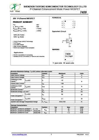
SHENZHEN TUOFENG SEMICONDUCTOR TECHNOLOGY CO.,LTD P-Channel Enhancement Mode Power MOSFET 7409 PDFN3X3-8L 30V P-Channel MOSFET 1 8 PRODUCT SUMMARY 2 7 VDS -30V 3 6 ID (at VGS=-10V) -32A 4 5 RDS(ON) (at VGS=-10V)
7409b.pdf

SHENZHEN TUOFENG SEMICONDUCTOR TECHNOLOGY CO.,LTD PDFN 3x3 Plastic-Encapsulate MOSFETS 7409B P-Channel Enhancement Mode Power MOSFET PDFN3X3-8L Description The 7409B uses advanced trench technology to provide 1 8 excellent RDS(ON), low gate charge and operation with gate 2 7 3 6 voltages as low as 4.5V. 4 5 General Features Equivalent Cir cuit VDS = -30V,ID = -25A
tw7404fj.pdf
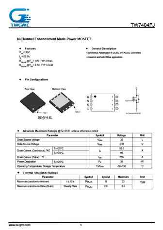
TW7404FJ N-Channel Enhancement Mode Power MOSFET Features General Description VDS = 30V, Synchronus Rectification in DC/DC and AC/DC Converters ID = 83.5A Industrial and Motor Drive applications RDS(ON) @VGS= 10V, TYP 2.5m RDS(ON) @VGS= 4.5V, TYP 3.3m Pin Configurations DFN5*6-8L Absolute Maximum Ratings @T =25 unless otherwise noted A Para
tw7408fn.pdf
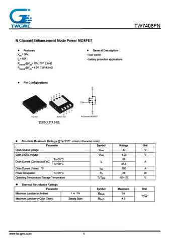
TW7408FN N-Channel Enhancement Mode Power MOSFET Features General Description VDS = 30V, load switch ID = 68A battery protection applications RDS(ON) @VGS= 10V, TYP 2.9m RDS(ON) @VGS= 4.5V, TYP 4.8m Pin Configurations TDFN3.3*3.3-8L Absolute Maximum Ratings @T =25 unless otherwise noted A Parameter Symbol Ratings Unit Drain-Source Voltage
tw7407fl-y.pdf
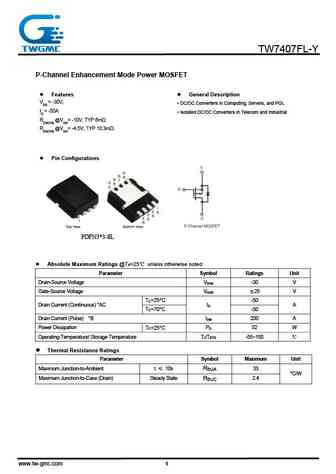
TW7407FL-Y P-Channel Enhancement Mode Power MOSFET Features General Description VDS = -30V, DC/DC Converters in Computing, Servers, and POL ID = -50A Isolated DC/DC Converters in Telecom and Industrial RDS(ON) @VGS= -10V, TYP 6m RDS(ON) @VGS= -4.5V, TYP 10.3m Pin Configurations PDFN3*3-8L Absolute Maximum Ratings @T =25 unless otherwise noted
se7401u.pdf
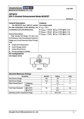
SHANGHAI July 2009 MICROELECTRONICS CO., LTD. SE7401U 20V P-Channel Enhancement-Mode MOSFET Revision B General Description Features The MOSFETs from SINO-IC provide For a single mosfet the best combination of fast switching, low VDS = -20 V on-resistance and cost-effectiveness. RDS(ON) = 120m @ VGS=-4.50V @Ids=-2.0A RDS(ON) = 150m @ VGS=-2.50V @Ids=-1.8A Gene
se7401p.pdf
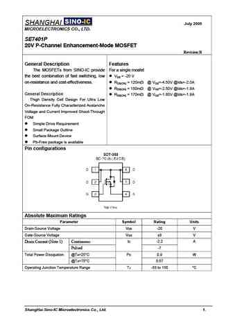
SHANGHAI July 2009 MICROELECTRONICS CO., LTD. SE7401P 20V P-Channel Enhancement-Mode MOSFET Revision B General Description Features The MOSFETs from SINO-IC provide For a single mosfet the best combination of fast switching, low VDS = -20 V on-resistance and cost-effectiveness. RDS(ON) = 120m @ VGS=-4.50V @Ids=-2.0A RDS(ON) = 150m @ VGS=-2.50V @Ids=-1.8A Gene
ao7401.pdf

AO7401 www.VBsemi.tw P-Channel 20 V (D-S) MOSFET FEATURES PRODUCT SUMMARY Halogen-free According to IEC 61249-2-21 VDS (V) RDS(on) ( )ID (A)c Qg (Typ.) Definition 0.080 at VGS = - 4.5 V - 3.1 TrenchFET Power MOSFET 4.3 nC - 20 0.100 at VGS = - 2.5 V - 2.3 100 % Rg Tested Compliant to RoHS Directive 2002/95/EC APPLICATIONS Load Switch DC/DC Converter
ao7400.pdf
AO7400 www.VBsemi.tw N-Channel 20 V (D-S) MOSFET FEATURES PRODUCT SUMMARY Halogen-free According to IEC 61249-2-21 VDS (V) RDS(on) ( )ID (A)a Qg (Typ.) Definition 0.036 at VGS = 10 V 4 TrenchFET Power MOSFET 20 0.040 at VGS = 4.5 V 3.8 4 nC Typical ESD Protection 2000 V HBM 0.048 at VGS = 2.5 V 3.6 100 % Rg Tested Compliant to RoHS Directive 2002/95/EC AP
irf7404tr.pdf
IRF7404TR www.VBsemi.tw P-Channel 20-V (D-S) MOSFET FEATURES PRODUCT SUMMARY Halogen-free According to IEC 61249-2-21 VDS (V) RDS(on) ( )ID (A) Qg (Typ.) Definition a 0.015 at VGS = - 4.5 V TrenchFET Power MOSFET - 13 a 100 % Rg Tested 0.026 at VGS = - 2.5 V - 20 20 nC - 10 Built in ESD Protection with Zener Diode 0.065 at VGS = - 1.8 V - 8 Typical
ao7407.pdf
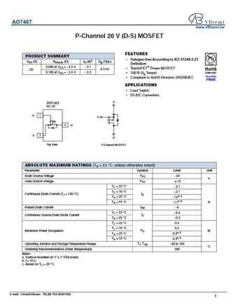
AO7407 www.VBsemi.tw P-Channel 20 V (D-S) MOSFET FEATURES PRODUCT SUMMARY Halogen-free According to IEC 61249-2-21 VDS (V) RDS(on) ( )ID (A)c Qg (Typ.) Definition 0.080 at VGS = - 4.5 V - 3.1 TrenchFET Power MOSFET 4.3 nC - 20 0.100 at VGS = - 2.5 V - 2.3 100 % Rg Tested Compliant to RoHS Directive 2002/95/EC APPLICATIONS Load Switch DC/DC Converter
ao7407.pdf
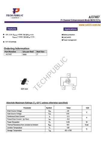
A O7 4 07 P-Channel Enhancement-Mode MOS FETs www.sot23.com.tw Features Applications (typ) @VGS =4.5V. -20V, -2.3A, RDS(ON) =100m Battery protection RDS(ON) = 125m (typ) @VGS = 2.5V. Load switch Power management SOT-323 package. Ordering Information Part Number Qty per Reel Reel Size AO7407 3000 7 D S G SOT-323 Absolute Maximum Ratings (TA=25 C unless ot
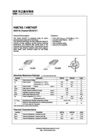
hm740 hm740f.pdf
740 / 740F 400V N-Channel MOSFET General Description Features This Power MOSFET is produced using SL semi s 10.5A, 400V, RDS(on) = 0.55 @VGS = 10 V advanced planar stripe DMOS technology. Low gate charge ( typical 30nC) This advanced technology has been especially tailored to Fast switching minimize on-state resistance, provide superior switching 100% avalanche
irf740.pdf
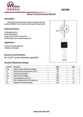
Silicon N-Channel Power MOSFET Description The IRF740 uses advanced technology and design to provide excellent RDS(ON). It can be used in a wide variety of applications. General Features VDS=400V,ID=10A Low ON Resistance Low Reverse transfer capacitances 100% Single Pulse avalanche energy Test Application Power switching application Adapter and charger Electrical C
2sa740.pdf
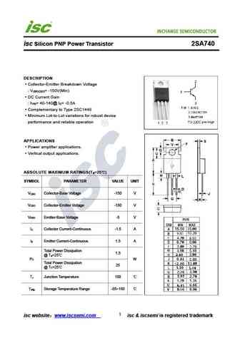
isc Silicon PNP Power Transistor 2SA740 DESCRIPTION Collector-Emitter Breakdown Voltage V = -150V(Min) (BR)CEO DC Current Gain h = 40-140@ I = -0.5A FE C Complementary to Type 2SC1448 Minimum Lot-to-Lot variations for robust device performance and reliable operation APPLICATIONS Power amplifier applications. Vertical output applications. ABSOLUTE MAXIMUM RATINGS(T
irfb7740.pdf
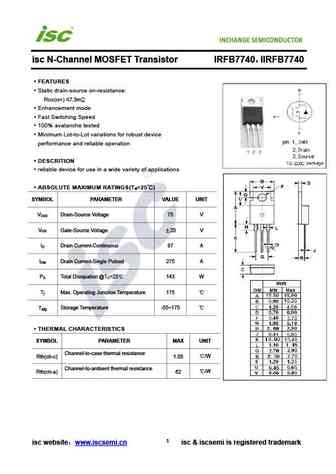
isc N-Channel MOSFET Transistor IRFB7740 IIRFB7740 FEATURES Static drain-source on-resistance RDS(on) 7.3m Enhancement mode Fast Switching Speed 100% avalanche tested Minimum Lot-to-Lot variations for robust device performance and reliable operation DESCRITION reliable device for use in a wide variety of applications ABSOLUTE MAXIMUM RATINGS(T =25 ) a
irfr7740.pdf
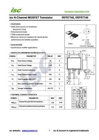
isc N-Channel MOSFET Transistor IRFR7740, IIRFR7740 FEATURES Static drain-source on-resistance RDS(on) 7.2m Enhancement mode 100% avalanche tested Minimum Lot-to-Lot variations for robust device performance and reliable operation DESCRITION Synchronous rectifier applications ABSOLUTE MAXIMUM RATINGS(T =25 ) a SYMBOL PARAMETER VALUE UNIT V Drain-Source Volta
2n6740.pdf
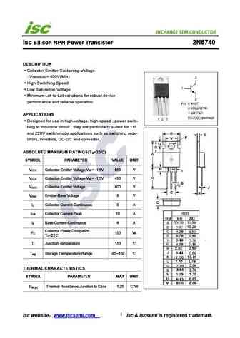
isc Silicon NPN Power Transistor 2N6740 DESCRIPTION Collector-Emitter Sustaining Voltage- V = 400V(Min) CEO(SUS) High Switching Speed Low Saturation Voltage Minimum Lot-to-Lot variations for robust device performance and reliable operation APPLICATIONS Designed for use in high-voltage, high-speed , power switc- hing in inductive circuit , they are particularly suited for
2n6738 2n6739 2n6740.pdf
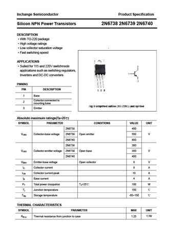
Inchange Semiconductor Product Specification Silicon NPN Power Transistors 2N6738 2N6739 2N6740 DESCRIPTION With TO-220 package High voltage ratings Low collector saturation voltage Fast switching speed APPLICATIONS Suited for 115 and 220V switchmode applications such as switching regulators, Inverters and DC-DC converters PINNING PIN DESCRIPTION 1 Base Co
2n3740a.pdf
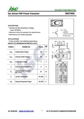
isc Silicon PNP Power Transistor 2N3740A DESCRIPTION Collector-Emitter Breakdown Voltage- V =-60V(Min) CEO Minimum Lot-to-Lot variations for robust device Performance and reliable operation APPLICATIONS Power amplifier and switching applications ABSOLUTE MAXIMUM RATINGS(Ta=25 ) UNI SYMBOL PARAMETER VALUE T V Collector-Base Voltage -60 V CBO V Collector-Emitter Voltage -
irf740a.pdf
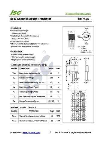
isc N-Channel Mosfet Transistor IRF740A FEATURES Drain Source Voltage- V = 400V(Min) DSS Static Drain-Source On-Resistance R = 0.55 (Max) DS(on) Fast Switching Speed Minimum Lot-to-Lot variations for robust device performance and reliable operation DESCRITION Switch mode power supply Uninterruptable power supply High speed power switching ABSOLUTE MAXIMUM
irf740fi.pdf
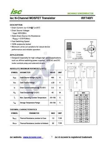
isc N-Channel MOSFET Transistor IRF740FI DESCRIPTION Drain Current I = 5.5A@ T =25 D C Drain Source Voltage- V = 400V(Min) DSS Static Drain-Source On-Resistance R = 0.55 (Max) DS(on) Fast Switching Speed 100% avalanche tested Minimum Lot-to-Lot variations for robust device performance and reliable operation APPLICATIONS Designed especially for high voltag
2sk3740.pdf
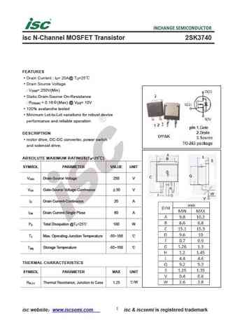
isc N-Channel MOSFET Transistor 2SK3740 FEATURES Drain Current I = 20A@ T =25 D C Drain Source Voltage V = 250V(Min) DSS Static Drain-Source On-Resistance R = 0.16 (Max) @ V = 10V DS(on) GS 100% avalanche tested Minimum Lot-to-Lot variations for robust device performance and reliable operation DESCRIPTION motor drive, DC-DC converter, power switch and soleno
2n3740 2n3741.pdf
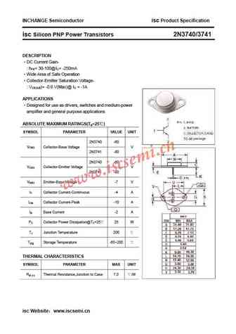
INCHANGE Semiconductor isc Product Specification isc Silicon PNP Power Transistors 2N3740/3741 DESCRIPTION DC Current Gain- hFE= 30-100@IC= -250mA Wide Area of Safe Operation Collector-Emitter Saturation Voltage- VCE(sat)= -0.6 V(Max)@ IC = -1A APPLICATIONS Designed for use as drivers, switches and medium-power amplifier and general purpose applications ABSOL
2sc2740.pdf
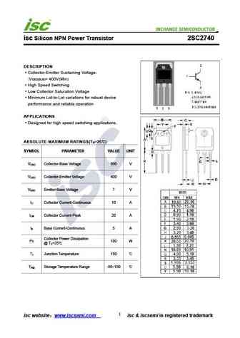
isc Silicon NPN Power Transistor 2SC2740 DESCRIPTION Collector-Emitter Sustaining Voltage- V = 400V(Min) CEO(SUS) High Speed Switching Low Collector Saturation Voltage Minimum Lot-to-Lot variations for robust device performance and reliable operation APPLICATIONS Designed for high speed switching applications. ABSOLUTE MAXIMUM RATINGS(T =25 ) a SYMBOL PARAMETER VALUE U
irf740.pdf
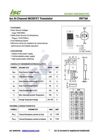
isc N-Channel MOSFET Transistor IRF740 FEATURES Drain Source Voltage- V = 400V(Min) DSS Static Drain-Source On-Resistance R = 0.55 (Max) DS(on) Fast Switching Speed Minimum Lot-to-Lot variations for robust device performance and reliable operation DESCRITION Switch mode power supply Uninterruptable power supply High speed power switching ABSOLUTE MAXIMUM
2n5740.pdf
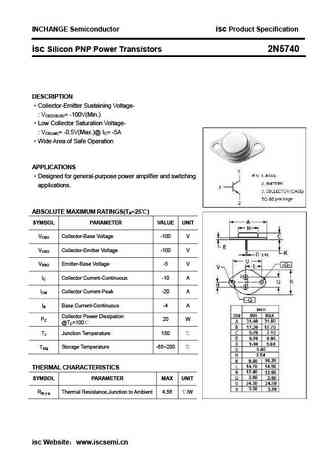
INCHANGE Semiconductor isc Product Specification isc Silicon PNP Power Transistors 2N5740 DESCRIPTION Collector-Emitter Sustaining Voltage- VCEO(SUS)= -100V(Min.) Low Collector Saturation Voltage- VCE(sat)= -0.5V(Max.)@ IC= -5A Wide Area of Safe Operation APPLICATIONS Designed for general-purpose power amplifier and switching applications. ABSOLUTE MAXIMUM RA
irfu7740.pdf
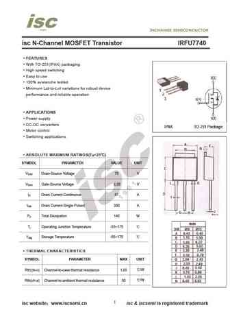
isc N-Channel MOSFET Transistor IRFU7740 FEATURES With TO-251(IPAK) packaging High speed switching Easy to use 100% avalanche tested Minimum Lot-to-Lot variations for robust device performance and reliable operation APPLICATIONS Power supply DC-DC converters Motor control Switching applications ABSOLUTE MAXIMUM RATINGS(T =25 ) a SYMBOL PARAMETER VALUE UN
Другие MOSFET... G3710 , 5N20A , 630A , 640 , 18N20 , 18N20A , 2N25 , 3N25 , IRF540 , 840 , 16N50F , 13N50F , 20N50 , 5N60F , 7N60F , 8N60A , 8N60AF .
History: R9521 | 840
🌐 : EN ES РУ

Список транзисторов
Обновления
MOSFET: ASD80R750E | ASD70R950E | ASD70R600E | ASD70R380E | ASD65R850E | ASD65R550E | ASD65R350E | ASD65R300E | ASD65R280E | ASD65R270E | ASD60R330E | ASD60R280E | ASB80R750E | ASB70R380E | ASB65R300E | ASB65R220E
Popular searches
bd139 | 2n4401 datasheet | irf640 | irf840 | irf740 | c945 transistor | irf640n | 2n3904