840. Аналоги и основные параметры
Наименование производителя: 840
Тип транзистора: MOSFET
Полярность: N
Предельные значения
Pd ⓘ - Максимальная рассеиваемая мощность: 139 W
|Vds|ⓘ - Максимально допустимое напряжение сток-исток: 500 V
|Vgs|ⓘ - Максимально допустимое напряжение затвор-исток: 30 V
|Id| ⓘ - Максимально допустимый постоянный ток стока: 9 A
Tj ⓘ - Максимальная температура канала: 150 °C
Электрические характеристики
tr ⓘ - Время нарастания: 70 ns
Cossⓘ - Выходная емкость: 130 pf
RDSonⓘ - Сопротивление сток-исток открытого транзистора: 0.85 Ohm
Тип корпуса: TO220
Аналог (замена) для 840
- подборⓘ MOSFET транзистора по параметрам
840 даташит
840.pdf
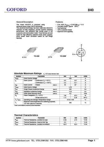
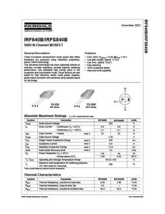
GOFORD 840 General Description Features This Power MOSFET is produced using 9.0A, 500V, RDS(on) = 0.85 @VGS = 10 V advanced planar stripe DMOS technology. Low gate charge ( typical 30nC) This advanced technology has been especially tailored to Fast switching minimize on-state resistance, provide superior switching 100% avalanche tested performance, and withstand high
ntmfd6h840nlt1g.pdf
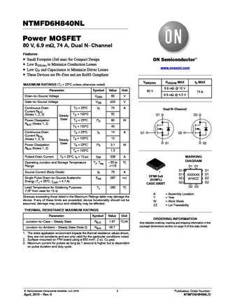
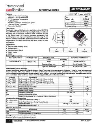
NTMFD6H840NL Power MOSFET 80 V, 6.9 mW, 74 A, Dual N-Channel Features Small Footprint (5x6 mm) for Compact Design Low RDS(on) to Minimize Conduction Losses www.onsemi.com Low QG and Capacitance to Minimize Driver Losses These Devices are Pb-Free and are RoHS Compliant V(BR)DSS RDS(ON) MAX ID MAX MAXIMUM RATINGS (TJ = 25 C unless otherwise noted) 6.9 mW @ 10 V Parame
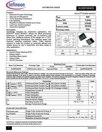
auirfn8405tr.pdf
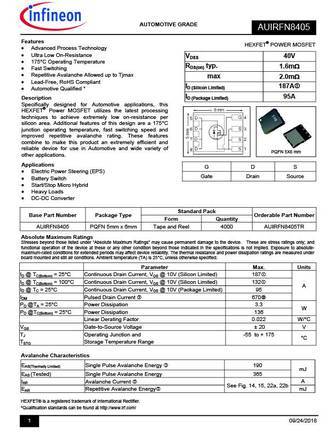
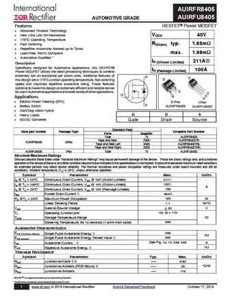
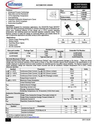
AUTOMOTIVE GRADE AUIRFN8405 Features HEXFET POWER MOSFET Advanced Process Technology Ultra Low On-Resistance VDSS 40V 175 C Operating Temperature RDS(on) typ. 1.6m Fast Switching Repetitive Avalanche Allowed up to Tjmax max 2.0m Lead-Free, RoHS Compliant ID (Silicon Limited) 187A Automotive Qualified *
irf840 irf841 irf840fi irf841fi.pdf

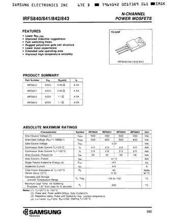
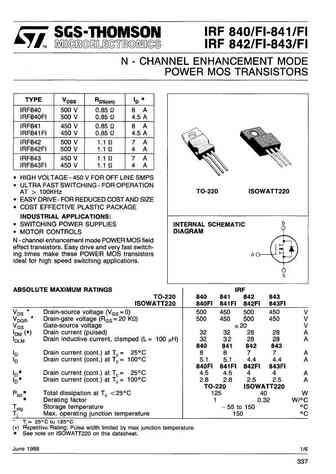
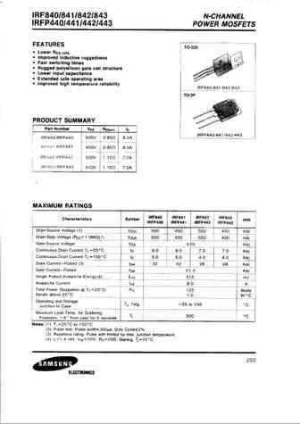
IRF840/FI IRF841/FI N - CHANNEL ENHANCEMENT MODE POWER MOS TRANSISTORS TYPE VDSS RDS(on) ID IRF840 500 V
mrf840.pdf
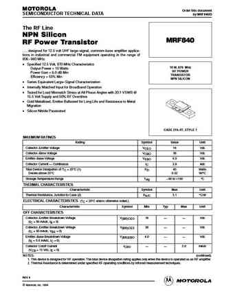
MOTOROLA Order this document SEMICONDUCTOR TECHNICAL DATA by MRF840/D The RF Line NPN Silicon MRF840 RF Power Transistor . . . designed for 12.5 volt UHF large signal, common base amplifier applica- tions in industrial and commercial FM equipment operating in the range of 806 960 MHz. Specified 12.5 Volt, 870 MHz Characteristics 10 W, 870 MHz Output Power = 10 Watts RF P
mrf840re.pdf

MOTOROLA Order this document SEMICONDUCTOR TECHNICAL DATA by MRF840/D The RF Line NPN Silicon MRF840 RF Power Transistor . . . designed for 12.5 volt UHF large signal, common base amplifier applica- tions in industrial and commercial FM equipment operating in the range of 806 960 MHz. Specified 12.5 Volt, 870 MHz Characteristics 10 W, 870 MHz Output Power = 10 Watts RF P
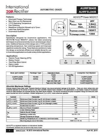
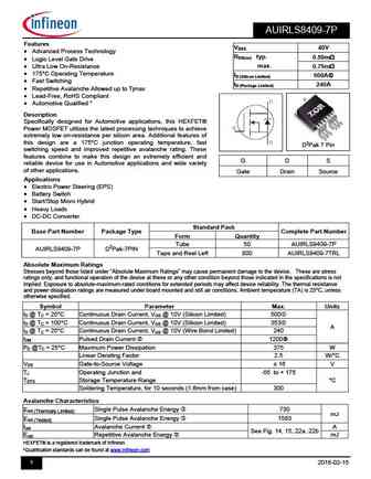
auirfs8403 auirfsl8403.pdf
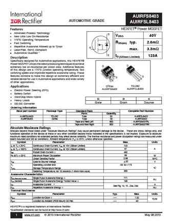
AUIRFS8403 AUTOMOTIVE GRADE AUIRFSL8403 HEXFET Power MOSFET Features l Advanced Process Technology D VDSS 40V l New Ultra Low On-Resistance l 175 C Operating Temperature RDS(on) typ. 2.6m l Fast Switching l Repetitive Avalanche Allowed up to Tjmax G max. 3.3m l Lead-Free, RoHS Compliant Automotive Qualified * S ID (Silicon Limited) 123A Description Specifically desi
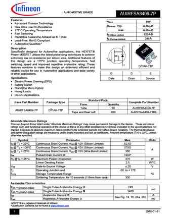
auirfs8409-7p.pdf
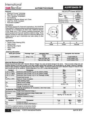
AUIRFS8409-7P AUTOMOTIVE GRADE Features HEXFET Power MOSFET l Advanced Process Technology 40V VDSS l New Ultra Low On-Resistance 0.55m RDS(on) typ. l 175 C Operating Temperature max. 0.75m l Fast Switching l Repetitive Avalanche Allowed up to Tjmax 522A ID (Silicon Limited) l Lead-Free, RoHS Compliant 240A ID (Package Limited) l Automotive Qualified * Description
irf840lcspbf irf840lclpbf.pdf
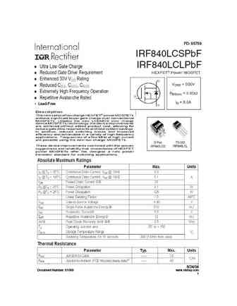
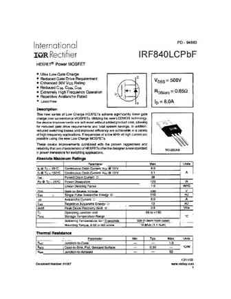
PD- 95759 IRF840LCSPbF IRF840LCLPbF Lead-Free 8/24/04 Document Number 91068 www.vishay.com 1 IRF840LCS/LPbF Document Number 91068 www.vishay.com 2 IRF840LCS/LPbF Document Number 91068 www.vishay.com 3 IRF840LCS/LPbF Document Number 91068 www.vishay.com 4 IRF840LCS/LPbF Document Number 91068 www.vishay.com 5 IRF840LCS/LPbF Document Number 91068 www.vishay.com
auirfb8409 auirfs8409 auirfsl8409.pdf
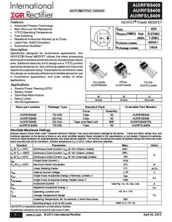
AUIRFB8409 AUTOMOTIVE GRADE AUIRFS8409 AUIRFSL8409 Features HEXFET Power MOSFET l Advanced Process Technology D l New Ultra Low On-Resistance VDSS 40V l 175 C Operating Temperature RDS(on) (SMD) typ. 0.97m l Fast Switching max. 1.2m l Repetitive Avalanche Allowed up to Tjmax G l Lead-Free, RoHS Compliant ID (Silicon Limited) 409A l Automotive Qualified * ID (Package Li
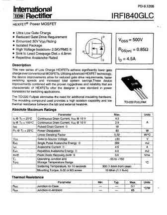
irfi840glcpbf.pdf
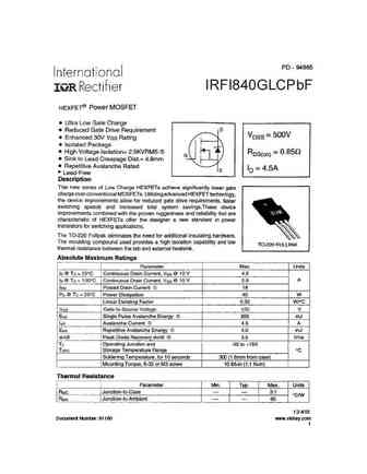
PD - 94865 IRFI840GLCPbF Lead-Free 12/4/03 Document Number 91160 www.vishay.com 1 IRFI840GLCPbF Document Number 91160 www.vishay.com 2 IRFI840GLCPbF Document Number 91160 www.vishay.com 3 IRFI840GLCPbF Document Number 91160 www.vishay.com 4 IRFI840GLCPbF Document Number 91160 www.vishay.com 5 IRFI840GLCPbF Document Number 91160 www.vishay.com 6 IRFI840GLCPbF
irfi840gpbf.pdf
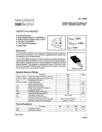
PD - 94864 IRFI840GPbF Lead-Free www.irf.com 1 12/03/03 IRFI840GPbF 2 www.irf.com IRFI840GPbF www.irf.com 3 IRFI840GPbF 4 www.irf.com IRFI840GPbF www.irf.com 5 IRFI840GPbF 6 www.irf.com IRFI840GPbF TO-220 Full-Pak Package Outline Dimensions are shown in millimeters (inches) TO-220 Full-Pak Part Marking Information E XAMP L E T H IS IS AN IR F I84 0G WIT H AS S E
auirfn8401.pdf
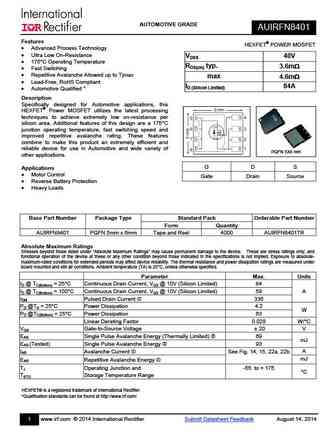
AUTOMOTIVE GRADE AUIRFN8401 Features HEXFET POWER MOSFET Advanced Process Technology Ultra Low On-Resistance VDSS 40V 175 C Operating Temperature RDS(on) typ. 3.6m Fast Switching Repetitive Avalanche Allowed up to Tjmax max 4.6m Lead-Free, RoHS Compliant ID (Silicon Limited) 84A Automotive Qualified * De
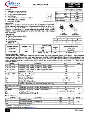
auirfr8401 auirfu8401.pdf
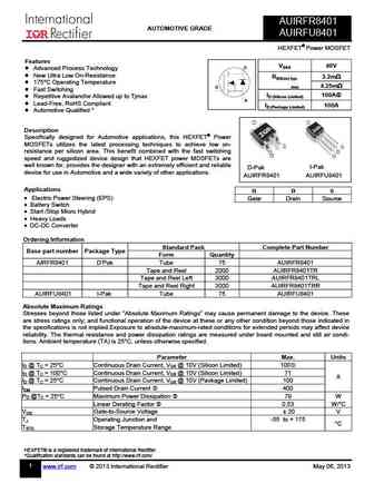
AUIRFR8401 AUTOMOTIVE GRADE AUIRFU8401 HEXFET Power MOSFET Features VDSS 40V D Advanced Process Technology New Ultra Low On-Resistance RDS(on) typ. 3.2m 175 C Operating Temperature 4.25m G max Fast Switching ID (Silicon Limited) 100A Repetitive Avalanche Allowed up to Tjmax S Lead-Free, RoHS Compliant ID
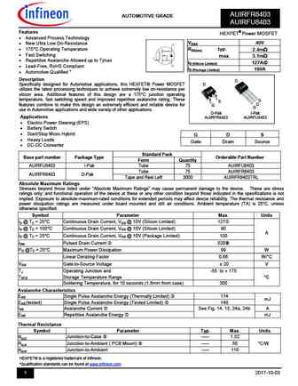
auirfr8403 auirfu8403.pdf
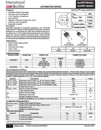
AUIRFR8403 AUIRFU8403 AUTOMOTIVE GRADE Features HEXFET Power MOSFET l Advanced Process Technology D VDSS 40V l New Ultra Low On-Resistance l 175 C Operating Temperature RDS(on) typ. 2.4m l Fast Switching l Repetitive Avalanche Allowed up to Tjmax max. 3.1m G l Lead-Free, RoHS Compliant ID (Silicon Limited) 127A l Automotive Qualified * Description S ID (Package L
auirfn8405.pdf
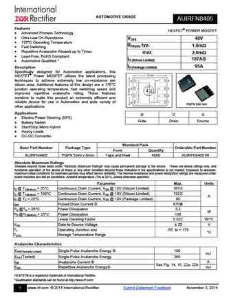
AUTOMOTIVE GRADE AUIRFN8405 Features HEXFET POWER MOSFET Advanced Process Technology Ultra Low On-Resistance VDSS 40V 175 C Operating Temperature RDS(on) typ. 1.6m Fast Switching Repetitive Avalanche Allowed up to Tjmax max 2.0m Lead-Free, RoHS Compliant ID (Silicon Limited) 187A Automotive Qualified *
irf840lcs.pdf
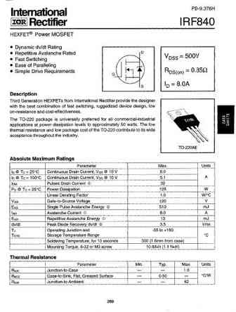
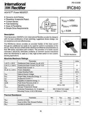
PD- 93766 IRF840LCS IRF840LCL HEXFET Power MOSFET Ultra Low Gate Charge D Reduced Gate Drive Requirement VDSS = 500V Enhanced 30V VGS Rating Reduced CISS, COSS, CRSS RDS(on) = 0.85 Extremely High Frequency Operation G Repetitive Avalanche Rated ID = 8.0A Description S This new series of low charge HEXFET power MOSFETs achieve significant lower gate charge over con
irf840lcpbf.pdf
PD - 94883 IRF840LCPbF Lead-Free 12/11/03 Document Number 91067 www.vishay.com 1 IRF840LCPbF Document Number 91067 www.vishay.com 2 IRF840LCPbF Document Number 91067 www.vishay.com 3 IRF840LCPbF Document Number 91067 www.vishay.com 4 IRF840LCPbF Document Number 91067 www.vishay.com 5 IRF840LCPbF Document Number 91067 www.vishay.com 6 IRF840LCPbF Document Nu
auirfn8403.pdf
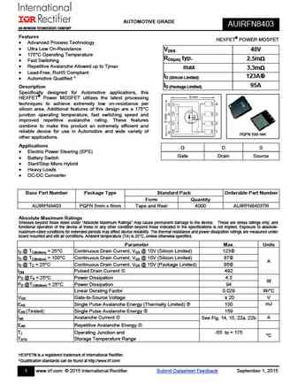
AUTOMOTIVE GRADE AUIRFN8403 Features HEXFET POWER MOSFET Advanced Process Technology Ultra Low On-Resistance VDSS 40V 175 C Operating Temperature RDS(on) typ. 2.5m Fast Switching Repetitive Avalanche Allowed up to Tjmax max 3.3m Lead-Free, RoHS Compliant ID (Silicon Limited) 123A Automotive Qualified *
auirfs8405 auirfsl8405.pdf
AUIRFS8405 AUTOMOTIVE GRADE AUIRFSL8405 Features HEXFET Power MOSFET l Advanced Process Technology D l New Ultra Low On-Resistance VDSS 40V l 175 C Operating Temperature RDS(on) typ.1.9m l Fast Switching max. 2.3m l Repetitive Avalanche Allowed up to Tjmax l Lead-Free, RoHS Compliant G ID (Silicon Limited) 193A l Automotive Qualified * ID (Package Limited) 120A S De
irf840apbf.pdf
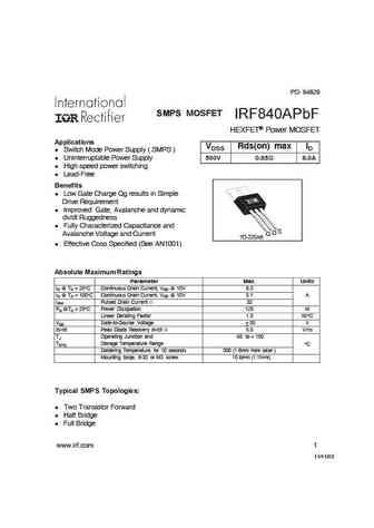
PD- 94829 SMPS MOSFET IRF840APbF HEXFET Power MOSFET Applications VDSS Rds(on) max ID l Switch Mode Power Supply ( SMPS ) l Uninterruptable Power Supply 500V 0.85 8.0A l High speed power switching l Lead-Free Benefits l Low Gate Charge Qg results in Simple Drive Requirement l Improved Gate, Avalanche and dynamic dv/dt Ruggedness l Fully Characterized Capacitance and S D A
irf840pbf.pdf
PD - 94882 IRF840PbF Lead-Free www.irf.com 1 12/10/03 IRF840PbF 2 www.irf.com IRF840PbF www.irf.com 3 IRF840PbF 4 www.irf.com IRF840PbF www.irf.com 5 IRF840PbF 6 www.irf.com IRF840PbF TO-220AB Package Outline Dimensions are shown in millimeters (inches) 10.54 (.415) - B - 3.78 (.149) 10.29 (.405) 2.87 (.113) 4.69 (.185) 3.54 (.139) 2.62 (.103) 4.20 (.165) - A -
auirfb8405.pdf
AUTOMOTIVE GRADE AUIRFB8405 Features HEXFET Power MOSFET Advanced Process Technology D New Ultra Low On-Resistance VDSS 40V 175 C Operating Temperature RDS(on) typ.2.1m Fast Switching Repetitive Avalanche Allowed up to Tjmax max. 2.5m Lead-Free, RoHS Compliant G ID (Silicon Limited) 185A Automotive Qualified * ID (Package Limited) 120A S
irf840aspbf irf840alpbf.pdf
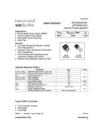
PD- 95143 IRF840ASPbF SMPS MOSFET IRF840ALPbF HEXFET Power MOSFET Applications VDSS RDS(on) max ID Switch Mode Power Supply (SMPS) Uninterruptible Power Supply 500V 0.85 8.0A High Speed Power Switching Lead-Free Benefits Low Gate Charge Qg Results in Simple Drive Requirement Improved Gate, Avalanche and Dynamic dv/dt Ruggedness Fully Characterized Capacitance and D
irf840spbf.pdf
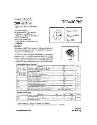
PD-95136 IRF840SPbF Lead-Free D2Pak 05/10/04 Document Number 91071 www.vishay.com 1 IRF840SPbF Document Number 91071 www.vishay.com 2 IRF840SPbF Document Number 91071 www.vishay.com 3 IRF840SPbF Document Number 91071 www.vishay.com 4 IRF840SPbF Document Number 91071 www.vishay.com 5 IRF840SPbF Document Number 91071 www.vishay.com 6 IRF840SPbF Document Numb
irf840a.pdf
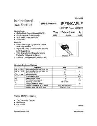
PD- 94829 SMPS MOSFET IRF840APbF HEXFET Power MOSFET Applications VDSS Rds(on) max ID l Switch Mode Power Supply ( SMPS ) l Uninterruptable Power Supply 500V 0.85 8.0A l High speed power switching l Lead-Free Benefits l Low Gate Charge Qg results in Simple Drive Requirement l Improved Gate, Avalanche and dynamic dv/dt Ruggedness l Fully Characterized Capacitance and S D A
auirfr8405 auirfu8405.pdf
AUIRFR8405 AUTOMOTIVE GRADE AUIRFU8405 Features HEXFET Power MOSFET l Advanced Process Technology l New Ultra Low On-Resistance VDSS 40V l 175 C Operating Temperature RDS(on) typ. 1.65m l Fast Switching l Repetitive Avalanche Allowed up to Tjmax max. 1.98m l Lead-Free, RoHS Compliant l Automotive Qualified * ID (Silicon Limited) 211A Description Specifically designed for A
auirfb8407 auirfs8407 auirfsl8407.pdf
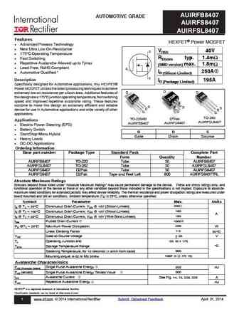
AUIRFB8407 AUTOMOTIVE GRADE AUIRFS8407 AUIRFSL8407 Features HEXFET Power MOSFET l Advanced Process Technology l New Ultra Low On-Resistance VDSS 40V D l 175 C Operating Temperature RDS(on) typ. 1.4m l Fast Switching l Repetitive Avalanche Allowed up to Tjmax (SMD version) max. 1.8m l Lead-Free, RoHS Compliant G 250A ID (Silicon Limited) Automotive Qualified * S
auirfs8407-7p.pdf
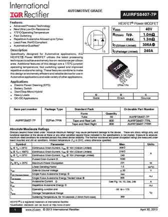
AUTOMOTIVE GRADE AUIRFS8407-7P Features HEXFET Power MOSFET Advanced Process Technology D New Ultra Low On-Resistance VDSS 40V 175 C Operating Temperature RDS(on) typ.1.0m Fast Switching Repetitive Avalanche Allowed up to Tjmax max. 1.3m Lead-Free, RoHS Compliant G ID (Silicon Limited) 306A Automotive Qualified * Description ID (Package L
auirfs8408 auirfsl8408.pdf
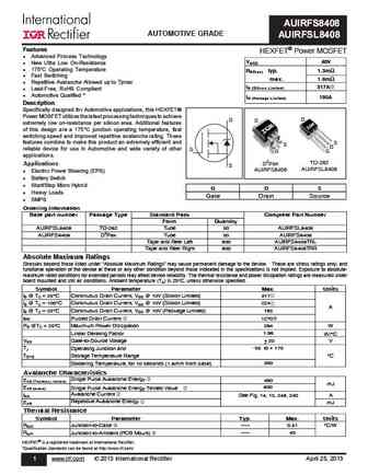
AUIRFS8408 AUTOMOTIVE GRADE AUIRFSL8408 Features HEXFET Power MOSFET l Advanced Process Technology VDSS 40V l New Ultra Low On-Resistance l 175 C Operating Temperature RDS(on) typ. 1.3m l Fast Switching max. 1.6m l Repetitive Avalanche Allowed up to Tjmax ID (Silicon Limited) 317A l Lead-Free, RoHS Compliant l Automotive Qualified * ID (Package Limited) 195A Descri
auirfs8408-7p.pdf
AUIRFS8408-7P AUTOMOTIVE GRADE Features HEXFET Power MOSFET l Advanced Process Technology 40V VDSS l New Ultra Low On-Resistance 0.70m RDS(on) typ. l 175 C Operating Temperature l Fast Switching max. 1.0m l Repetitive Avalanche Allowed up to Tjmax 397A ID (Silicon Limited) l Lead-Free, RoHS Compliant 240A ID (Package Limited) l Automotive Qualified * Description
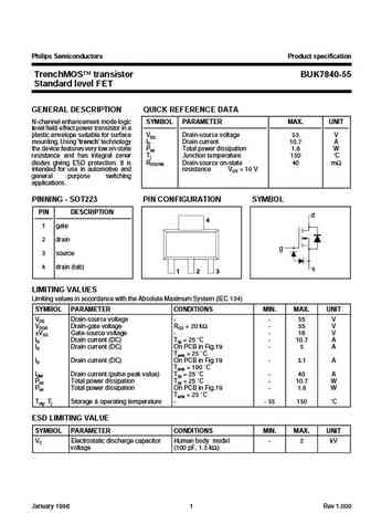
buk9840-55 2.pdf

Philips Semiconductors Product specification TrenchMOS transistor BUK9840-55 Logic level FET GENERAL DESCRIPTION QUICK REFERENCE DATA N-channel enhancement mode logic SYMBOL PARAMETER MAX. UNIT level field-effect power transistor in a plastic envelope suitable for surface VDS Drain-source voltage 55 V mounting. The device features very ID Drain current 10.7 A low on-state resistanc
bf840.pdf
DISCRETE SEMICONDUCTORS DATA SHEET BF840 NPN medium frequency transistor Product data sheet 2004 Jan 13 Supersedes data of 1999 Apr 12 NXP Semiconductors Product data sheet NPN medium frequency transistor BF840 FEATURES PINNING Low current (max. 25 mA) PIN DESCRIPTION Low voltage (max. 40 V). 1 base 2 emitter APPLICATIONS 3 collector AM mixers IF amplifiers i
lxe18400x 2.pdf
DISCRETE SEMICONDUCTORS DATA SHEET book, halfpage M3D039 LXE18400X NPN microwave power transistor 1999 Apr 22 Product specification Supersedes data of December 1994 Philips Semiconductors Product specification NPN microwave power transistor LXE18400X FEATURES QUICK REFERENCE DATA Microwave performance up to Tmb =25 C in a common emitter class AB Diffused emitter ballasting r
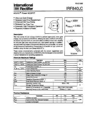
irf840 1.pdf
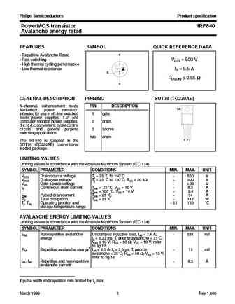
Philips Semiconductors Product specification PowerMOS transistor IRF840 Avalanche energy rated FEATURES SYMBOL QUICK REFERENCE DATA d Repetitive Avalanche Rated Fast switching VDSS = 500 V High thermal cycling performance Low thermal resistance ID = 8.5 A g RDS(ON) 0.85 s GENERAL DESCRIPTION PINNING SOT78 (TO220AB) N-channel, enhancement mode PIN DESCRIPT
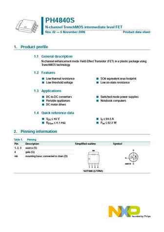
ph4840s.pdf

PH4840S N-channel TrenchMOS intermediate level FET Rev. 02 6 November 2006 Product data sheet 1. Product profile 1.1 General description N-channel enhancement mode Field-Effect Transistor (FET) in a plastic package using TrenchMOS technology. 1.2 Features Low thermal resistance SO8 equivalent area footprint Low threshold voltage Low on-state resistance 1.3 Applications DC-to-D
buk7840-55 1.pdf
Philips Semiconductors Product specification TrenchMOS transistor BUK7840-55 Standard level FET GENERAL DESCRIPTION QUICK REFERENCE DATA N-channel enhancement mode logic SYMBOL PARAMETER MAX. UNIT level field-effect power transistor in a plastic envelope suitable for surface VDS Drain-source voltage 55 V mounting. Using trench technology ID Drain current 10.7 A the device fea
irf840-fi irf841-fi.pdf
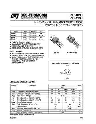
IRF840/FI IRF841/FI N - CHANNEL ENHANCEMENT MODE POWER MOS TRANSISTORS TYPE VDSS RDS(on) ID IRF840 500 V
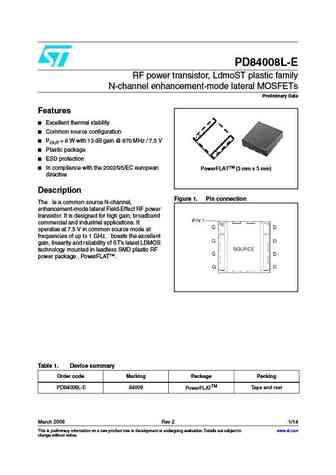
pd84006l-e.pdf
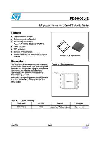
PD84006L-E RF power transistor, LDmoST plastic family Features Excellent thermal stability Common source configuration Broadband performances POUT = 6 W with 13 dB gain @ 870 MHz Plastic package ESD protection Supplied in tape and reel In compliance with the 2002/95/EC european PowerFLATTM (5mm x 5mm) directive Description Figure 1. Pin connection
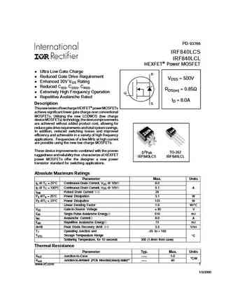
irf840.pdf
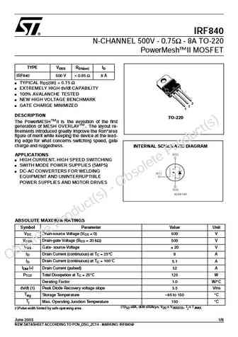
IRF840 N-CHANNEL 500V - 0.75 - 8ATO-220 PowerMesh II MOSFET TYPE VDSS RDS(on) ID IRF840 500 V
std840dn40.pdf
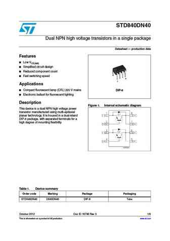
STD840DN40 Dual NPN high voltage transistors in a single package Datasheet production data Features Low VCE(sat) Simplified circuit design Reduced component count 8 Fast switching speed 4 1 Applications Compact fluorescent lamp (CFL) 220 V mains DIP-8 Electronic ballast for fluorescent lighting Description Figure 1. Internal schematic diagram This de
pd84002.pdf
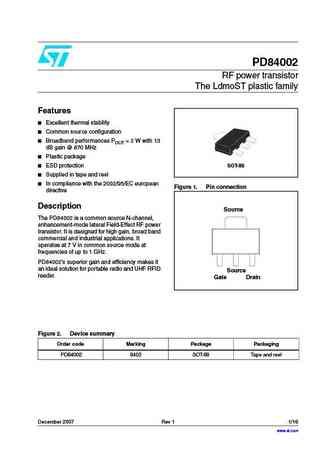
PD84002 RF power transistor The LdmoST plastic family Features Excellent thermal stability Common source configuration Broadband performances POUT = 2 W with 13 dB gain @ 870 MHz Plastic package SOT-89 ESD protection Supplied in tape and reel In compliance with the 2002/95/EC european Figure 1. Pin connection directive Description Source The PD840
irf840f.pdf

IRF840/FI IRF841/FI N - CHANNEL ENHANCEMENT MODE POWER MOS TRANSISTORS TYPE VDSS RDS(on) ID IRF840 500 V
pd84008l-e.pdf
PD84008L-E RF power transistor, LdmoST plastic family N-channel enhancement-mode lateral MOSFETs Preliminary Data Features Excellent thermal stability Common source configuration POUT = 8 W with 13 dB gain @ 870 MHz / 7.5 V Plastic package ESD protection In compliance with the 2002/95/EC european PowerFLATTM (5 mm x 5 mm) directive Description Figure 1. Pi
irf840a.pdf
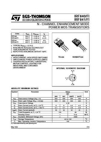
IRF840/FI IRF841/FI N - CHANNEL ENHANCEMENT MODE POWER MOS TRANSISTORS TYPE VDSS RDS(on) ID IRF840 500 V
pd84006-e.pdf
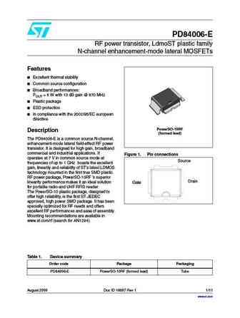
PD84006-E RF power transistor, LdmoST plastic family N-channel enhancement-mode lateral MOSFETs Features Excellent thermal stability Common source configuration Broadband performances POUT = 6 W with 13 dB gain @ 870 MHz Plastic package ESD protection In compliance with the 2002/95/EC european directive PowerSO-10RF Description (formed lead) The PD84
pd84010-e pd84010s-e.pdf
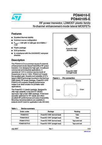
PD84010-E PD84010S-E RF power transistor, LDMOST plastic family N-channel enhancement-mode lateral MOSFETs Features Excellent thermal stability Common source configuration POUT = 10W with 14.3dB gain @ 870MHz / 7.5V Plastic package PowerSO-10RF (formed lead) ESD protection In compliance with the 2002/95/EC european directive Description The PD8401
pd84008-e pd84008s-e.pdf
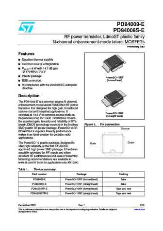
PD84008-E PD84008S-E RF power transistor, LdmoST plastic family N-channel enhancement-mode lateral MOSFETs Preliminary Data Features Excellent thermal stability Common source configuration POUT = 8 W with 14.7 dB gain @ 870 MHz / 7.5 V Plastic package PowerSO-10RF (formed lead) ESD protection In compliance with the 2002/95/EC european directive Descript
tpcp8404.pdf
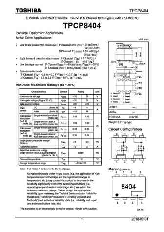
TPCP8404 TOSHIBA Field Effect Transistor Silicon P, N Channel MOS Type (U-MO /U-MOS ) TPCP8404 Portable Equipment Applications Motor Drive Applications Unit mm 0.33 0.05 Low drain-source ON-resistance P Channel RDS (ON) = 38 m (typ.) 0.05 M A 8 5 (VGS=-10V) N Channel RDS (ON) = 38 m (typ.) VGS=10V) High forward transfer admittance P Channel Yfs
2sc4840.pdf
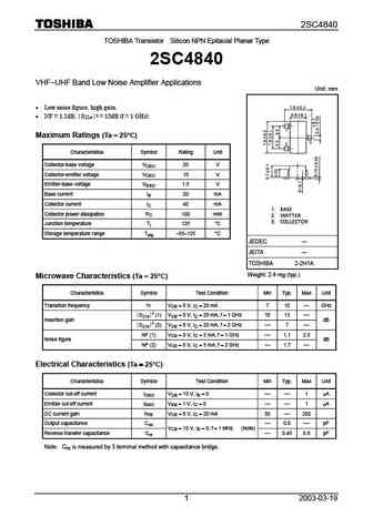
2SC4840 TOSHIBA Transistor Silicon NPN Epitaxial Planar Type 2SC4840 VHF UHF Band Low Noise Amplifier Applications Unit mm Low noise figure, high gain. NF = 1.1dB, S 2 = 13dB (f = 1 GHz) 21e Maximum Ratings (Ta = = 25 C) = = Characteristics Symbol Rating Unit Collector-base voltage VCBO 20 V Collector-emitter voltage VCEO 10 V Emitter-base voltage VEBO 1.5 V
tpc8407.pdf
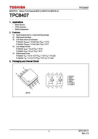
TPC8407 MOSFETs Silicon P-/N-Channel MOS (U-MOS /U-MOS -H) TPC8407 TPC8407 TPC8407 TPC8407 1. Applications 1. Applications 1. Applications 1. Applications Motor Drivers CCFL Inverters Mobile Equipments 2. Features 2. Features 2. Features 2. Features (1) Small footprint due to a small and thin package (2) High speed switching (3) Low drain-source on-resistance
tpc8406-h.pdf
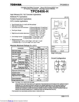
TPC8406-H TOSHIBA Field Effect Transistor Silicon P/N-Channel MOS Type (P-Channel N-Channel Ultra-High-Speed U-MOSIII) TPC8406-H High Efficiency DC DC Converter Applications Notebook PC Applications Unit mm Portable Equipment Applications CCFL Inverter Applications Small footprint due to a small and thin package High speed switching Low drain-source ON-resi
tpcp8405.pdf
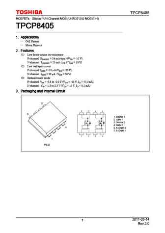
TPCP8405 MOSFETs Silicon P-/N-Channel MOS (U-MOS /U-MOS -H) TPCP8405 TPCP8405 TPCP8405 TPCP8405 1. Applications 1. Applications 1. Applications 1. Applications Cell Phones Motor Drivers 2. Features 2. Features 2. Features 2. Features (1) Low drain-source on-resistance P-channel RDS(ON) = 24 m (typ.) (VGS = -10 V), N-channel RDS(ON) = 20 m (typ.) (VGS = 10 V)
tpc8401.pdf
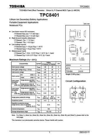
TPC8401 TOSHIBA Field Effect Transistor Silicon N, P Channel MOS Type (U-MOSII) TPC8401 Lithium Ion Secondary Battery Applications Portable Equipment Applications Unit mm Notebook PCs Low drain-source ON resistance P Channel RDS (ON) = 27 m (typ.) N Channel R = 14 m (typ.) DS (ON) High forward transfer admittance P Channel Yfs = 7 S (typ.) N Channel
tpcp8403.pdf
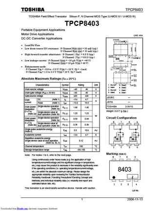
TPCP8403 TOSHIBA Field Effect Transistor Silicon P, N Channel MOS Type (U-MOS IV / U-MOS III) TPCP8403 Portable Equipment Applications Motor Drive Applications Unit mm DC-DC Converter Applications 0.33 0.05 0.05 M A 8 5 Lead(Pb)-Free Low drain-source ON resistance P Channel RDS (ON) = 55 m (typ.) N Channel RDS (ON) = 31 m (typ.) High forward trans
tpcp8407.pdf
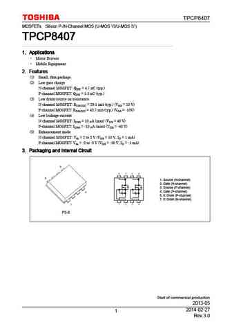
TPCP8407 MOSFETs Silicon P-/N-Channel MOS (U-MOS /U-MOS ) TPCP8407 TPCP8407 TPCP8407 TPCP8407 1. Applications 1. Applications 1. Applications 1. Applications Motor Drivers Mobile Equipment 2. Features 2. Features 2. Features 2. Features (1) Small, thin package (2) Low gate charge N-channel MOSFET QSW = 4.7 nC (typ.) P-channel MOSFET QSW = 5.5 nC (typ.) (3) Lo
tpc8404.pdf
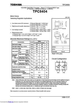
TPC8404 TOSHIBA Field Effect Transistor Silicon P, N Channel MOS Type (P Channel -MOSV/N Channel -MOSV) TPC8404 Motor Dreive Unit mm Switching Regulator Applications Low drain-source ON resistance P Channel RDS (ON) = 1.85 (typ.) N Channel RDS (ON) = 1.2 (typ.) High forward transfer admittance P Channel Yfs = 1.1 S (typ.) N Channel Yfs = 1.3 S (ty
tpcp8401.pdf
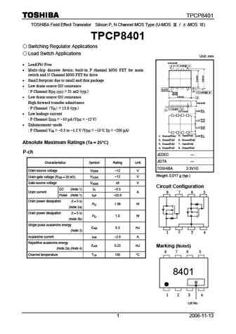
TPCP8401 TOSHIBA Field Effect Transistor Silicon P, N Channel MOS Type (U-MOS / -MOS ) TPCP8401 Switching Regulator Applications Load Switch Applications Unit mm 0.33 0.05 Lead(Pb)-Free 0.05 M A 8 5 Multi-chip discrete device; built-in P channel MOS FET for main switch and N Channel MOS FET for drive Small footprint due to small and thin pack
tpcp8406.pdf
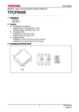
TPCP8406 MOSFETs Silicon P-/N-Channel MOS (U-MOS /U-MOS -H) TPCP8406 TPCP8406 TPCP8406 TPCP8406 1. Applications 1. Applications 1. Applications 1. Applications Cell Phones Motor Drivers 2. Features 2. Features 2. Features 2. Features (1) Low drain-source on-resistance P-channel RDS(ON) = 33 m (typ.) (VGS = -10 V), N-channel RDS(ON) = 24 m (typ.) (VGS = 10 V)
tpc8408.pdf
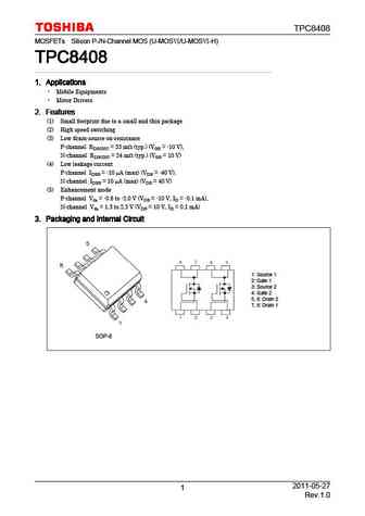
TPC8408 MOSFETs Silicon P-/N-Channel MOS (U-MOS /U-MOS -H) TPC8408 TPC8408 TPC8408 TPC8408 1. Applications 1. Applications 1. Applications 1. Applications Mobile Equipments Motor Drivers 2. Features 2. Features 2. Features 2. Features (1) Small footprint due to a small and thin package (2) High speed switching (3) Low drain-source on-resistance P-channel RDS(ON) =
tpc8405.pdf
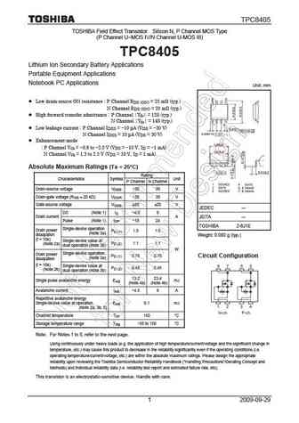
TPC8405 TOSHIBA Field Effect Transistor Silicon N, P Channel MOS Type (P Channel U-MOS IV/N Channel U-MOS III) TPC8405 Lithium Ion Secondary Battery Applications Portable Equipment Applications Notebook PC Applications Unit mm Low drain-source ON resistance P Channel RDS (ON) = 25 m (typ.) N Channel RDS (ON) = 20 m (typ.) High forward transfer admittance P Cha
tpcp8402.pdf
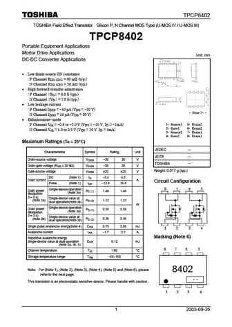
TPCP8402 TOSHIBA Field Effect Transistor Silicon P, N Channel MOS Type (U-MOS IV / U-MOS III) TPCP8402 Portable Equipment Applications Mortor Drive Applications Unit mm DC-DC Converter Applications Low drain-source ON resistance P Channel R = 60 m (typ.) DS (ON) N Channel R = 38 m (typ.) DS (ON) High forward transfer admittance P Channel Y = 6.0
tpcf8402.pdf
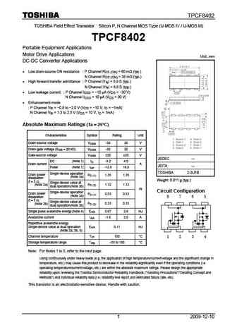
TPCF8402 TOSHIBA Field Effect Transistor Silicon P, N Channel MOS Type (U-MOS IV / U-MOS III) TPCF8402 Portable Equipment Applications Motor Drive Applications Unit mm DC-DC Converter Applications Low drain-source ON resistance P Channel RDS (ON) = 60 m (typ.) N Channel RDS (ON) = 38 m (typ.) High forward transfer admittance P Channel Yfs = 5.9 S (typ.)
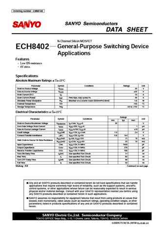
ech8402.pdf
Ordering number ENN8148 ECH8402 N-Channel Silicon MOSFET General-Purpose Switching Device ECH8402 Applications Features Low ON-resistance. 4V drive. Specifications Absolute Maximum Ratings at Ta=25 C Parameter Symbol Conditions Ratings Unit Drain-to-Source Voltage VDSS 30 V Gate-to-Source Voltage VGSS 20 V Drain Current (DC) ID 10 A Drain Current (Pulse) IDP PW 10
2sk1840.pdf
Ordering number EN4635 N-Channel Enhancement Silicon MOSFET 2SK1840 Analog Switch Applications Features Package Dimensions Large yfs . unit mm Enhancement type. 2024B Low ON resistance. [2SK1840] 0.4 0.16 3 0 to 0.1 1 0.95 2 0.95 1.9 2.9 1 Gate 2 Drain 3 Source SANYO CP Specifications Absolute Maximum Ratings at Ta = 25 C Parameter Symbol Condi
2sd1840.pdf
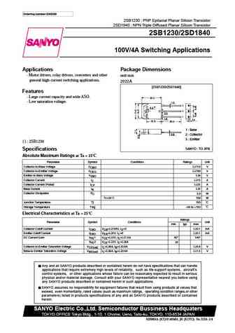
Ordering number EN3259 2SB1230 PNP Epitaxial Planar Silicon Transistor 2SD1840 NPN Triple Diffused Planar Silicon Transistor 2SB1230/2SD1840 100V/4A Switching Applications Applications Package Dimensions Motor drivers, relay drivers, converters and other unit mm general high-current switching applications. 2022A [2SB1230/2SD1840] Features Large current capacity and wide
fdmq8403.pdf
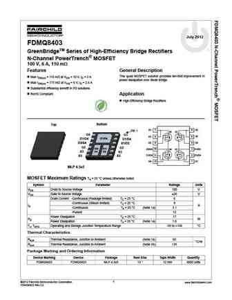
July 2012 FDMQ8403 GreenBridgeTM Series of High-Efficiency Bridge Rectifiers N-Channel PowerTrench MOSFET 100 V, 6 A, 110 m Features General Description This quad MOSFET solution provides ten-fold improvement in Max rDS(on) = 110 m at VGS = 10 V, ID = 3 A power dissipation over diode bridge. Max rDS(on) = 175 m at VGS = 6 V, ID = 2.4 A Substantial efficiency benefit in PD
fds8840nz.pdf
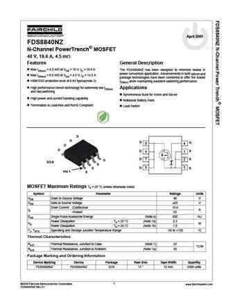
April 2009 FDS8840NZ N-Channel PowerTrench MOSFET 40 V, 18.6 A, 4.5 m Features General Description Max rDS(on) = 4.5 m at VGS = 10 V, ID = 18.6 A The FDS8840NZ has been designed to minimize losses in power conversion application. Advancements in both silicon and Max rDS(on) = 6.0 m at VGS = 4.5 V, ID = 14.9 A package technologies have been combined to offer the lowest
2sa1840.pdf
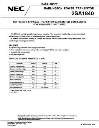
DATA SHEET DARLINGTON POWER TRANSISTOR 2SA1840 PNP SILICON EPITAXIAL TRANSISTOR (DARLINGTON CONNECTION) FOR HIGH-SPEED SWITCHING The 2SA1840 is a high-speed Darlington power transistor. This transistor is ideal for high-precision control such as PWM control for pulse motors or brushless motors in OA and FA equipment. In addition, this transistor features a package that can be auto-mounte
bf840.pdf
Important notice Dear Customer, On 7 February 2017 the former NXP Standard Product business became a new company with the tradename Nexperia. Nexperia is an industry leading supplier of Discrete, Logic and PowerMOS semiconductors with its focus on the automotive, industrial, computing, consumer and wearable application markets In data sheets and application notes which still contain
ph4840s.pdf
PH4840S N-channel TrenchMOS intermediate level FET Rev. 02 6 November 2006 Product data sheet 1. Product profile 1.1 General description N-channel enhancement mode Field-Effect Transistor (FET) in a plastic package using TrenchMOS technology. 1.2 Features Low thermal resistance SO8 equivalent area footprint Low threshold voltage Low on-state resistance 1.3 Applications DC-to-D
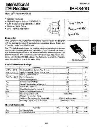
irfs840a.pdf
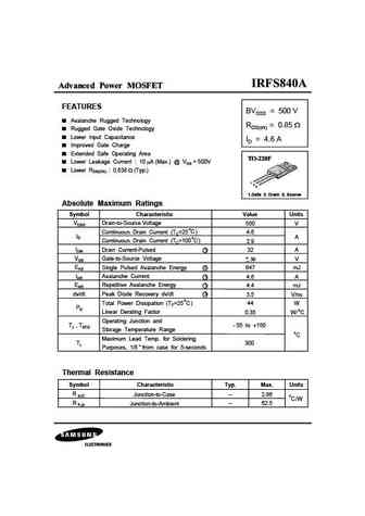
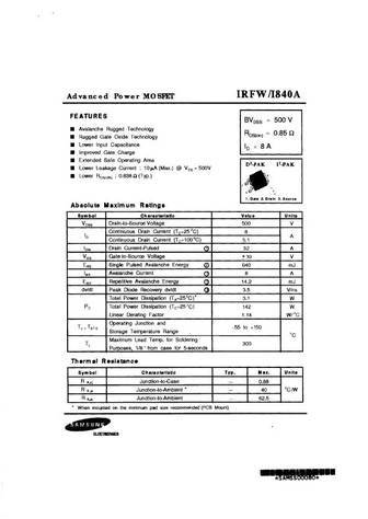
Advanced Power MOSFET FEATURES BVDSS = 500 V Avalanche Rugged Technology RDS(on) = 0.85 Rugged Gate Oxide Technology Lower Input Capacitance ID = 4.6 A Improved Gate Charge Extended Safe Operating Area Lower Leakage Current 10 A (Max.) @ VDS = 500V Lower RDS(ON) 0.638 (Typ.) 1 2 3 1.Gate 2. Drain 3. Source Absolute Maximum Ratings Symbol Characteristic V
irfw840a.pdf
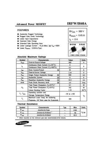
Advanced Power MOSFET FEATURES BVDSS = 500 V Avalanche Rugged Technology RDS(on) = 0.85 Rugged Gate Oxide Technology Lower Input Capacitance ID = 8 A Improved Gate Charge Extended Safe Operating Area Lower Leakage Current 10 A (Max.) @ VDS = 500V 2 Lower RDS(ON) 0.638 (Typ.) 1 1 2 3 3 1. Gate 2. Drain 3. Source Absolute Maximum Ratings Symbol Char
irf840a.pdf
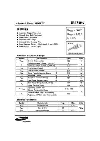
Advanced Power MOSFET FEATURES BVDSS = 500 V Avalanche Rugged Technology RDS(on) = 0.85 Rugged Gate Oxide Technology Lower Input Capacitance ID = 8 A Improved Gate Charge Extended Safe Operating Area Lower Leakage Current 10 A (Max.) @ VDS = 500V Lower RDS(ON) 0.638 (Typ.) 1 2 3 1.Gate 2. Drain 3. Source Absolute Maximum Ratings Symbol Characteristic Val
bf840.pdf
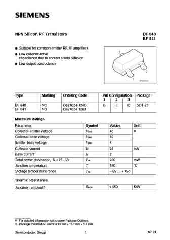
NPN Silicon RF Transistors BF 840 BF 841 Suitable for common emitter RF, IF amplifiers Low collector-base capacitance due to contact shield diffusion Low output conductance Type Marking Ordering Code Pin Configuration Package1) 1 2 3 BF 840 NC Q62702-F1240 B E C SOT-23 BF 841 ND Q62702-F1287 Maximum Ratings Parameter Symbol Values Unit Collector-emitter voltage VCE0 40 V Collect
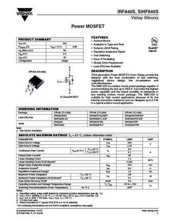
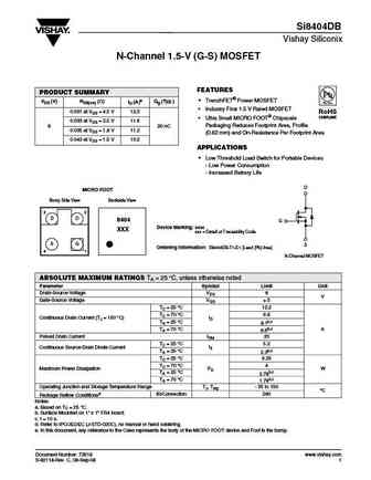
sihf840a.pdf
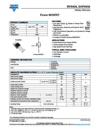
IRF840A, SiHF840A Vishay Siliconix Power MOSFET FEATURES PRODUCT SUMMARY Low Gate Charge Qg Results in Simple Drive VDS (V) 500 Requirement Available RDS(on) ( )VGS = 10 V 0.85 Improved Gate, Avalanche and Dynamic dV/dt RoHS* Qg (Max.) (nC) 38 COMPLIANT Ruggedness Qgs (nC) 9.0 Fully Characterized Capacitance and Avalanche Voltage Qgd (nC) 18 and Current Configura
irf840a sihf840a.pdf

IRF840A, SiHF840A Vishay Siliconix Power MOSFET FEATURES PRODUCT SUMMARY Low Gate Charge Qg Results in Simple Drive VDS (V) 500 Requirement Available RDS(on) ( )VGS = 10 V 0.85 Improved Gate, Avalanche and Dynamic dV/dt RoHS* Qg (Max.) (nC) 38 COMPLIANT Ruggedness Qgs (nC) 9.0 Fully Characterized Capacitance and Avalanche Voltage Qgd (nC) 18 and Current Configura
irfi840glcpbf sihfi840glc.pdf
IRFI840GLC, SiHFI840GLC Vishay Siliconix Power MOSFET FEATURES PRODUCT SUMMARY Ultra Low Gate Charge VDS (V) 500 Reduced Gate Drive Requirement Available RDS(on) ( )VGS = 10 V 0.85 Enhanced 30 V VGS Rating RoHS* Qg (Max.) (nC) 39 COMPLIANT Isolated Package Qgs (nC) 10 High Voltage Isolation = 2.5 kVRMS (t = 60 s; f = 60 Hz) Qgd (nC) 19 Sink to Lead Cr
irf840b.pdf
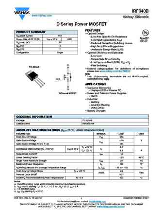
IRF840B www.vishay.com Vishay Siliconix D Series Power MOSFET FEATURES PRODUCT SUMMARY Optimal Design VDS (V) at TJ max. 550 - Low Area Specific On-Resistance RDS(on) max. at 25 C ( ) VGS = 10 V 0.85 - Low Input Capacitance (Ciss) Qg (max.) (nC) 30 - Reduced Capacitive Switching Losses Qgs (nC) 4 - High Body Diode Ruggedness Qgd (nC) 7 - Avalanche Energy Rated (UIS) Con
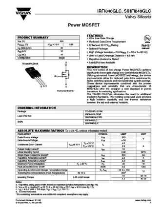
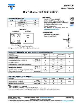
irf840lc irf840lcpbf sihf840lc.pdf
IRF840LC, SiHF840LC Vishay Siliconix Power MOSFET FEATURES PRODUCT SUMMARY Ultra Low Gate Charge VDS (V) 500 Reduced Gate Drive Requirement Available RDS(on) ( )VGS = 10 V 0.85 Enhanced 30 V VGS Rating RoHS* COMPLIANT Reduced Ciss, Coss, Crss Qg (Max.) (nC) 39 Extremely High Frequency Operation Qgs (nC) 10 Repetitive Avalanche Rated Qgd (nC) 19 Com
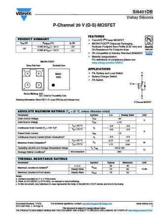
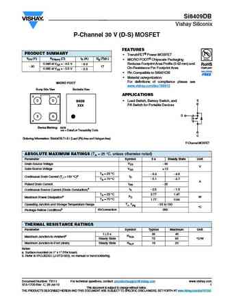
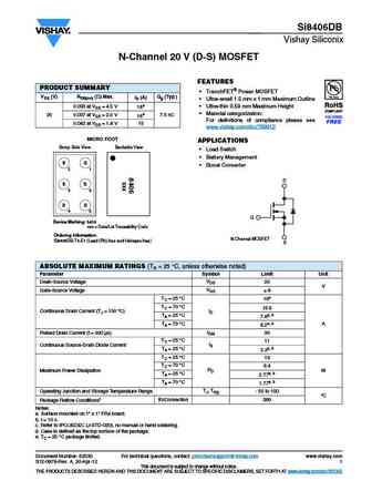
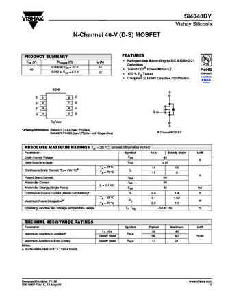
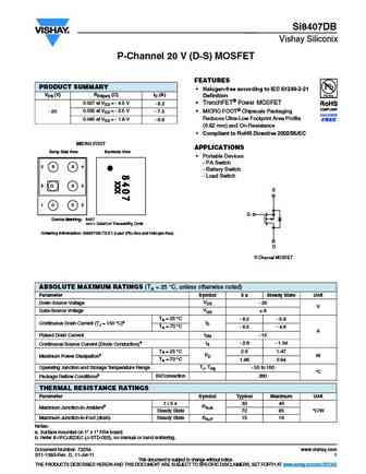
si4840bdy.pdf
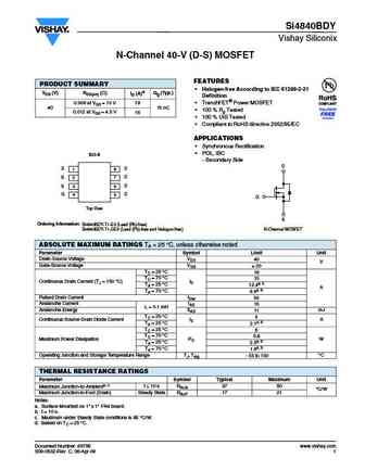
Si4840BDY Vishay Siliconix N-Channel 40-V (D-S) MOSFET FEATURES PRODUCT SUMMARY Halogen-free According to IEC 61249-2-21 VDS (V) RDS(on) ( ) ID (A)d Qg (Typ.) Definition 0.009 at VGS = 10 V TrenchFET Power MOSFET 19 40 15 nC 100 % Rg Tested 0.012 at VGS = 4.5 V 16 100 % UIS Tested Compliant to RoHS directive 2002/95/EC APPLICATIONS Synchronou
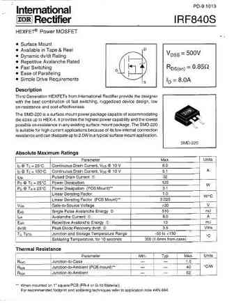
irf840s sihf840s.pdf
IRF840S, SiHF840S Vishay Siliconix Power MOSFET FEATURES PRODUCT SUMMARY Surface Mount VDS (V) 500 Available in Tape and Reel Available RDS(on) ( )VGS = 10 V 0.85 Dynamic dV/dt Rating RoHS* Qg (Max.) (nC) 63 COMPLIANT Repetitive Avalanche Rated Qgs (nC) 9.3 Fast Switching Qgd (nC) 32 Ease of Paralleling Configuration Single Simple Drive Requireme
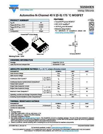
sq4840ey.pdf
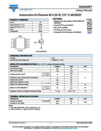
SQ4840EY www.vishay.com Vishay Siliconix Automotive N-Channel 40 V (D-S) 175 C MOSFET FEATURES PRODUCT SUMMARY Halogen-free According to IEC 61249-2-21 VDS (V) 40 Definition RDS(on) ( ) at VGS = 10 V 0.009 TrenchFET Power MOSFET RDS(on) ( ) at VGS = 4.5 V 0.012 AEC-Q101 Qualified ID (A) 20.7 100 % Rg and UIS Tested Configuration Single Compliant to Ro
irf840as sihf840as irf840al sihf840al.pdf
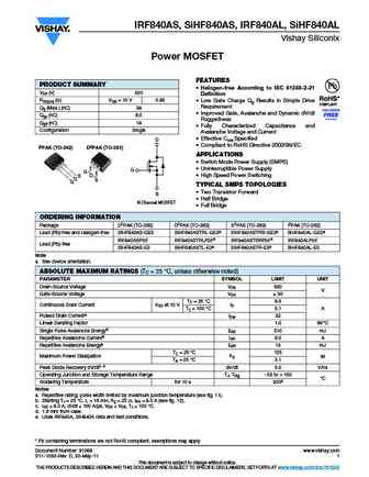
IRF840AS, SiHF840AS, IRF840AL, SiHF840AL Vishay Siliconix Power MOSFET FEATURES PRODUCT SUMMARY Halogen-free According to IEC 61249-2-21 VDS (V) 500 Definition RDS(on) ( )VGS = 10 V 0.85 Low Gate Charge Qg Results in Simple Drive Requirement Qg (Max.) (nC) 38 Improved Gate, Avalanche and Dynamic dV/dt Qgs (nC) 9.0 Ruggedness Qgd (nC) 18 Fully Characterized Capa
sihfi840g.pdf

IRFI840G, SiHFI840G Vishay Siliconix Power MOSFET FEATURES PRODUCT SUMMARY Isolated Package VDS (V) 500 Available High Voltage Isolation = 2.5 kVRMS (t = 60 s, RDS(on) ( )VGS = 10 V 0.85 f = 60 Hz) RoHS* COMPLIANT Qg (Max.) (nC) 67 Sink to Lead Creepage Distance = 4.8 mm Qgs (nC) 10 Dynamic dV/dt Rating Qgd (nC) 34 Low Thermal Resistance Configuration Si
irfi840glc sihfi840glc.pdf

IRFI840GLC, SiHFI840GLC Vishay Siliconix Power MOSFET FEATURES PRODUCT SUMMARY Ultra Low Gate Charge VDS (V) 500 Reduced Gate Drive Requirement Available RDS(on) ( )VGS = 10 V 0.85 Enhanced 30 V VGS Rating RoHS* Qg (Max.) (nC) 39 COMPLIANT Isolated Package Qgs (nC) 10 High Voltage Isolation = 2.5 kVRMS (t = 60 s; f = 60 Hz) Qgd (nC) 19 Sink to Lead Cr
irf840lclpbf irf840lcspbf sihf840lcl sihf840lcs.pdf
IRF840LCS, IRF840LCL, SiHF840LCS, SiHF840LCL Vishay Siliconix Power MOSFET FEATURES PRODUCT SUMMARY Halogen-free According to IEC 61249-2-21 Definition VDS (V) 500 Ultra Low Gate Charge RDS(on) ( )VGS = 10 V 0.85 Reduced Gate Drive Requirement Qg (Max.) (nC) 39 Enhanced 30 V VGS Rating Reduced Ciss, Coss, Crss Qgs (nC) 10 Extremely High Frequency Operatio
irfi840g sihfi840g.pdf
IRFI840G, SiHFI840G Vishay Siliconix Power MOSFET FEATURES PRODUCT SUMMARY Isolated Package VDS (V) 500 Available High Voltage Isolation = 2.5 kVRMS (t = 60 s, RDS(on) ( )VGS = 10 V 0.85 f = 60 Hz) RoHS* COMPLIANT Qg (Max.) (nC) 67 Sink to Lead Creepage Distance = 4.8 mm Qgs (nC) 10 Dynamic dV/dt Rating Qgd (nC) 34 Low Thermal Resistance Configuration Si
irf840alpbf irf840aspbf sihf840al sihf840as.pdf

IRF840AS, SiHF840AS, IRF840AL, SiHF840AL Vishay Siliconix Power MOSFET FEATURES PRODUCT SUMMARY Halogen-free According to IEC 61249-2-21 VDS (V) 500 Definition RDS(on) ( )VGS = 10 V 0.85 Low Gate Charge Qg Results in Simple Drive Requirement Qg (Max.) (nC) 38 Improved Gate, Avalanche and Dynamic dV/dt Qgs (nC) 9.0 Ruggedness Qgd (nC) 18 Fully Characterized Capa
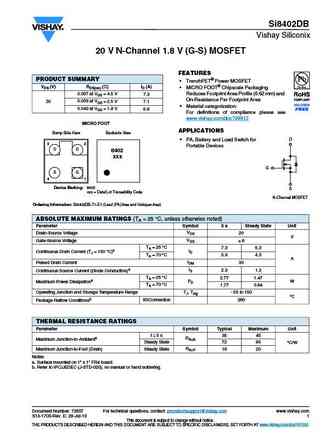
si4840dy.pdf
Si4840DY Vishay Siliconix N-Channel 40-V (D-S) MOSFET FEATURES PRODUCT SUMMARY Halogen-free According to IEC 61249-2-21 VDS (V) RDS(on) ( )ID (A) Definition 0.009 at VGS = 10 V 14 TrenchFET Power MOSFET 40 0.012 at VGS = 4.5 V 12 100 % Rg Tested Compliant to RoHS Directive 2002/95/EC SO-8 D S D 1 8 2 7 S D S 3 6 D G 4 5 G D Top View S Order
irf840spbf sihf840s.pdf
IRF840S, SiHF840S Vishay Siliconix Power MOSFET FEATURES PRODUCT SUMMARY Halogen-free According to IEC 61249-2-21 VDS (V) 500 Definition Surface Mount RDS(on) ( )VGS = 10 V 0.85 Available in Tape and Reel Qg (Max.) (nC) 63 Dynamic dV/dt Rating Qgs (nC) 9.3 Repetitive Avalanche Rated Qgd (nC) 32 Fast Switching Ease of Paralleling Configuration Sin
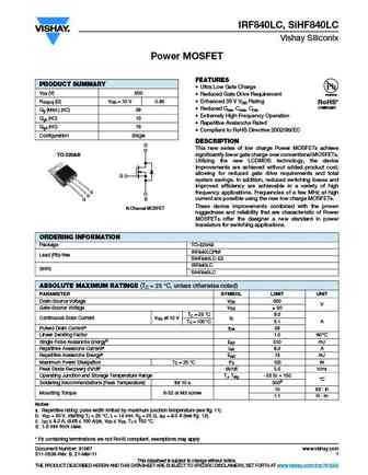
irf840 sihf840.pdf

IRF840, SiHF840 Vishay Siliconix Power MOSFET FEATURES PRODUCT SUMMARY Dynamic dV/dt Rating VDS (V) 500 Available Repetitive Avalanche Rated RDS(on) ( )VGS = 10 V 0.85 RoHS* Fast Switching Qg (Max.) (nC) 63 COMPLIANT Ease of Paralleling Qgs (nC) 9.3 Qgd (nC) 32 Simple Drive Requirements Configuration Single Compliant to RoHS Directive 2002/95/EC D DE
irf840lpbf sihf840l.pdf

IRF840L, SiHF840L Vishay Siliconix Power MOSFET FEATURES PRODUCT SUMMARY Halogen-free According to IEC 61249-2-21 VDS (V) 500 Definition Dynamic dV/dt Rating RDS(on) ( )VGS = 10 V 0.85 Repetitive Avalanche Rated Qg (Max.) (nC) 63 Fast Switching Qgs (nC) 9.3 Ease of Paralleling Qgd (nC) 32 Simple Drive Requirements Configuration Single Compliant to
irf840lc sihf840lc.pdf

IRF840LC, SiHF840LC Vishay Siliconix Power MOSFET FEATURES PRODUCT SUMMARY Ultra Low Gate Charge VDS (V) 500 Reduced Gate Drive Requirement Available RDS(on) ( )VGS = 10 V 0.85 Enhanced 30 V VGS Rating RoHS* COMPLIANT Reduced Ciss, Coss, Crss Qg (Max.) (nC) 39 Extremely High Frequency Operation Qgs (nC) 10 Repetitive Avalanche Rated Qgd (nC) 19 Com
si4840bd.pdf

Si4840BDY Vishay Siliconix N-Channel 40-V (D-S) MOSFET FEATURES PRODUCT SUMMARY Halogen-free According to IEC 61249-2-21 VDS (V) RDS(on) ( ) ID (A)d Qg (Typ.) Definition 0.009 at VGS = 10 V TrenchFET Power MOSFET 19 40 15 nC 100 % Rg Tested 0.012 at VGS = 4.5 V 16 100 % UIS Tested Compliant to RoHS directive 2002/95/EC APPLICATIONS Synchronou
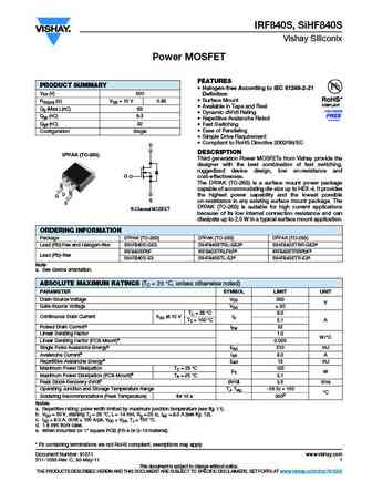
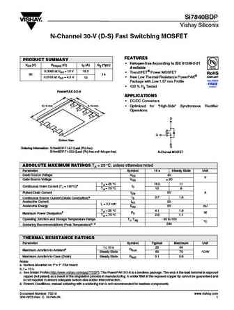
si7840dp.pdf
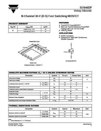
Si7840DP Vishay Siliconix N-Channel 30-V (D-S) Fast Switching MOSFET FEATURES PRODUCT SUMMARY D TrenchFETr Power MOSFET VDS (V) rDS(on) (W) ID (A) D New Low Thermal Resistance PowerPAKr Package with Low 1.07-mm Profile 0.0095 @ VGS = 10 V 18 30 30 D 100% Rg Tested 0.014 @ VGS = 4.5 V 15 APPLICATIONS D DC/DC Converters D Optimized for High-Side Synchronous Rectifier Operat
sqs840en.pdf
SQS840EN www.vishay.com Vishay Siliconix Automotive N-Channel 40 V (D-S) 175 C MOSFET FEATURES PRODUCT SUMMARY TrenchFET power MOSFET VDS (V) 40 AEC-Q101 qualified d RDS(on) ( ) at VGS = 10 V 0.0200 100 % Rg and UIS tested RDS(on) ( ) at VGS = 4.5 V 0.0300 Material categorization ID (A) 12 For definitions of compliance please see Configuration Single www.v
si7840bdp.pdf
Si7840BDP Vishay Siliconix N-Channel 30-V (D-S) Fast Switching MOSFET FEATURES PRODUCT SUMMARY Halogen-free According to IEC 61249-2-21 VDS (V) RDS(on) ( )ID (A) Qg (Typ.) Available 0.0085 at VGS = 10 V 16.5 TrenchFET Power MOSFET 30 14 0.0105 at VGS = 4.5 V New Low Thermal Resistance PowerPAK 13 Package with Low 1.07 mm Profile 100 % Rg Tested PowerP
sihf840.pdf
IRF840, SiHF840 Vishay Siliconix Power MOSFET FEATURES PRODUCT SUMMARY Dynamic dV/dt Rating VDS (V) 500 Available Repetitive Avalanche Rated RDS(on) ( )VGS = 10 V 0.85 RoHS* Fast Switching Qg (Max.) (nC) 63 COMPLIANT Ease of Paralleling Qgs (nC) 9.3 Qgd (nC) 32 Simple Drive Requirements Configuration Single Compliant to RoHS Directive 2002/95/EC D DE
irf840l sihf840l.pdf
IRF840L, SiHF840L Vishay Siliconix Power MOSFET FEATURES PRODUCT SUMMARY Halogen-free According to IEC 61249-2-21 VDS (V) 500 Definition Dynamic dV/dt Rating RDS(on) ( )VGS = 10 V 0.85 Repetitive Avalanche Rated Qg (Max.) (nC) 63 Fast Switching Qgs (nC) 9.3 Ease of Paralleling Qgd (nC) 32 Simple Drive Requirements Configuration Single Compliant to
sqj840ep.pdf
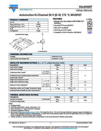
SQJ840EP www.vishay.com Vishay Siliconix Automotive N-Channel 30 V (D-S) 175 C MOSFET FEATURES PRODUCT SUMMARY Halogen-free According to IEC 61249-2-21 VDS (V) 30 Definition RDS(on) ( ) at VGS = 10 V 0.0093 TrenchFET Power MOSFET RDS(on) ( ) at VGS = 4.5 V 0.0138 AEC-Q101 Qualifiedd ID (A) 30 100 % Rg and UIS Tested Configuration Single Compliant to RoH
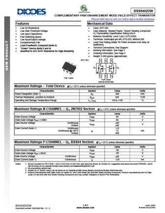
zxtn08400bff.pdf
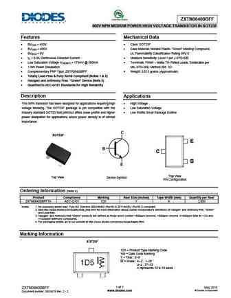
ZXTN08400BFF 400V NPN MEDIUM POWER HIGH VOLTAGE TRANSISTOR IN SOT23F Features Mechanical Data BVCEX > 450V Case SOT23F BVCEO > 400V Case Material Molded Plastic. Green Molding Compound. BVECO > 6V UL Flammability Classification Rating 94V-0 IC = 0.5A Continuous Collector Current Moisture Sensitivity Level 1 per J-STD-020 Low Saturation Volt
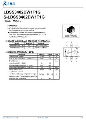
bss8402dw.pdf
BSS8402DW COMPLEMENTARY PAIR ENHANCEMENT MODE FIELD EFFECT TRANSISTOR Please click here to visit our online spice models database. Features Mechanical Data Low On-Resistance Case SOT-363 Low Gate Threshold Voltage Case Material Molded Plastic. Green Molding Compound. UL Flammability Classification Rating 94V-0 Low Input Capacitance Moisture Sensitiv
zxtp08400bff.pdf
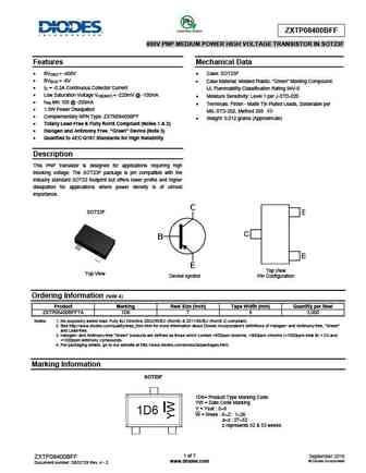
ZXTP08400BFF 400V PNP MEDIUM POWER HIGH VOLTAGE TRANSISTOR IN SOT23F Features Mechanical Data BVCEO > -400V Case SOT23F BVECO > -6V Case Material Molded Plastic. Green Molding Compound. IC = -0.2A Continuous Collector Current UL Flammability Classification Rating 94V-0 Low Saturation Voltage VCE(SAT)
buk9840-55 2.pdf
Philips Semiconductors Product specification TrenchMOS transistor BUK9840-55 Logic level FET GENERAL DESCRIPTION QUICK REFERENCE DATA N-channel enhancement mode logic SYMBOL PARAMETER MAX. UNIT level field-effect power transistor in a plastic envelope suitable for surface VDS Drain-source voltage 55 V mounting. The device features very ID Drain current 10.7 A low on-state resistanc
bts840s2.pdf
Preliminary Data PROFET BTS 840S2 Smart High-Side Power Switch Two Channels 2 x 30m Current Sense Product Summary Package Operating Voltage Vbb(on) 5.0...34V P-DSO-20-12 (Power SO 20) Active channels one two parallel On-state Resistance RON 30m 15m Load Current (ISO) IL(ISO) 12A 24A Current Limitation IL(SCr) 24A 24A General Description N channel vertical power MO
auirfsa8409-7p.pdf
AUTOMOTIVE GRADE AUIRFSA8409-7P Features VDSS 40V Advanced Process Technology RDS(on) typ. 0.50m New Ultra Low On-Resistance max. 175 C Operating Temperature 0.69m Fast Switching ID (Silicon Limited) 523A Repetitive Avalanche Allowed up to Tjmax ID (Package Limited) 360A Lead-Free, RoHS Compliant Automotive Qualified * Descr
auirfr8401 auirfu8401.pdf
AUIRFR8401 AUTOMOTIVE GRADE AUIRFU8401 Features HEXFET Power MOSFET Advanced Process Technology VDSS 40V New Ultra Low On-Resistance 175 C Operating Temperature RDS(on) typ. 3.2m Fast Switching max. 4.25m Repetitive Avalanche Allowed up to Tjmax ID (Silicon Limited) 100A Lead-Free, RoHS Compliant ID (Package Limited) 100A
auirfr8403 auirfu8403.pdf
AUIRFR8403 AUTOMOTIVE GRADE AUIRFU8403 Features HEXFET Power MOSFET Advanced Process Technology VDSS 40V New Ultra Low On-Resistance 175 C Operating Temperature RDS(on) typ. 2.4m Fast Switching max. 3.1m Repetitive Avalanche Allowed up to Tjmax ID (Silicon Limited) 127A Lead-Free, RoHS Compliant ID (Package Limited) 100A
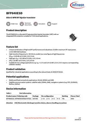
bfr840l3rhesd.pdf
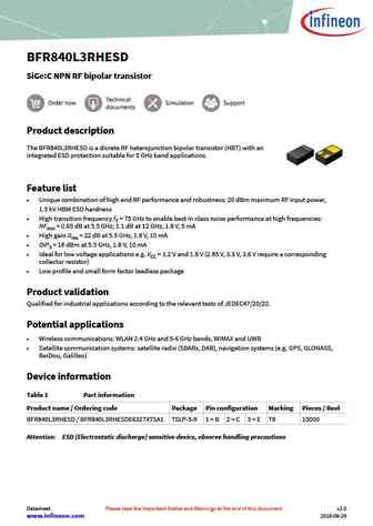
BFR840L3RHESD SiGe C NPN RF bipolar transistor Product description The BFR840L3RHESD is a dicrete RF heterojunction bipolar transistor (HBT) with an integrated ESD protection suitable for 5 GHz band applications. Feature list Unique combination of high end RF performance and robustness 20 dBm maximum RF input power, 1.5 kV HBM ESD hardness High transition frequency fT = 75 GHz
auirfn8405.pdf
AUTOMOTIVE GRADE AUIRFN8405 Features HEXFET POWER MOSFET Advanced Process Technology Ultra Low On-Resistance VDSS 40V 175 C Operating Temperature RDS(on) typ. 1.6m Fast Switching Repetitive Avalanche Allowed up to Tjmax max 2.0m Lead-Free, RoHS Compliant ID (Silicon Limited) 187A Automotive Qualified *
bfp840esd.pdf
BFP840ESD SiGe C NPN RF bipolar transistor Product description The BFP840ESD is a discrete RF heterojunction bipolar transistor (HBT) with an integrated ESD protection suitable for 5 GHz band applications. Feature list Unique combination of high end RF performance and robustness 20 dBm maximum RF input power, 1.5 kV HBM ESD hardness High transition frequency fT = 80 GHz to enab
auirls8409-7p.pdf
AUIRLS8409-7P Features VDSS 40V Advanced Process Technology RDS(on) typ. 0.50m Logic Level Gate Drive max. Ultra Low On-Resistance 0.75m 175 C Operating Temperature ID (Silicon Limited) 500A Fast Switching ID (Package Limited) 240A Repetitive Avalanche Allowed up to Tjmax Lead-Free, RoHS Compliant Automotive Qualified *
bsd840n.pdf
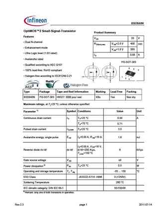
BSD840N OptiMOS 2 Small-Signal-Transistor Product Summary Features V 20 V DS Dual N-channel R V =2.5 V 400 m DS(on),max GS Enhancement mode V =1.8 V 560 GS Ultra Logic level (1.8V rated) I 0.88 A D Avalanche rated PG-SOT-363 Qualified according to AEC Q101 6 5 4 100% lead-free; RoHS compliant Halogen-free according to IEC61249-2-21 1 2 3
auirfr8405 auirfu8405.pdf
AUIRFR8405 AUTOMOTIVE GRADE AUIRFU8405 Features VDSS 40V Advanced Process Technology RDS(on) typ. 1.65m New Ultra Low On-Resistance max. 1.98m 175 C Operating Temperature ID (Silicon Limited) 211A Fast Switching ID (Package Limited) 100A Repetitive Avalanche Allowed up to Tjmax Lead-Free, RoHS Compliant D Automotive
bfp840fesd.pdf
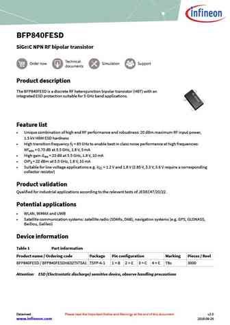
BFP840FESD SiGe C NPN RF bipolar transistor Product description The BFP840FESD is a discrete RF heterojunction bipolar transistor (HBT) with an integrated ESD protection suitable for 5 GHz band applications. Feature list Unique combination of high end RF performance and robustness 20 dBm maximum RF input power, 1.5 kV HBM ESD hardness High transition frequency fT = 85 GHz to en
ncv8401.pdf
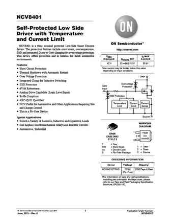
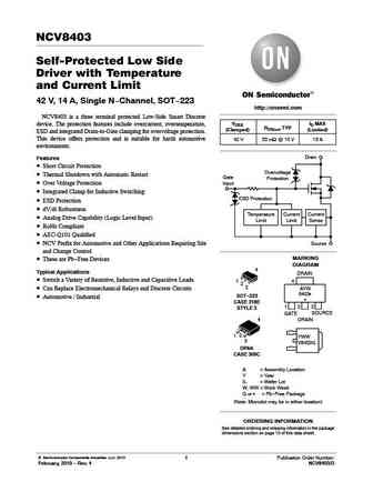
NCV8401 Self-Protected Low Side Driver with Temperature and Current Limit NCV8401 is a three terminal protected Low-Side Smart Discrete device. The protection features include overcurrent, overtemperature, http //onsemi.com ESD and integrated Drain-to-Gate clamping for overvoltage protection. This device offers protection and is suitable for harsh automotive VDSS ID MAX (Clamped) RDS(
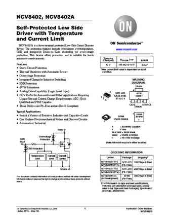
ncv8402.pdf
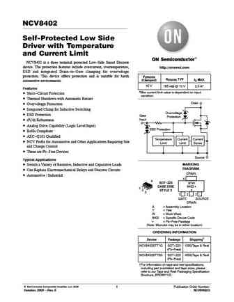
NCV8402 Self-Protected Low Side Driver with Temperature and Current Limit NCV8402 is a three terminal protected Low-Side Smart Discrete device. The protection features include overcurrent, overtemperature, http //onsemi.com ESD and integrated Drain-to-Gate clamping for overvoltage protection. This device offers protection and is suitable for harsh V(BR)DSS RDS(ON) TYP ID MAX (Clampe
ntmfd6h840nl.pdf
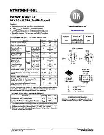
NTMFD6H840NL Power MOSFET 80 V, 6.9 mW, 74 A, Dual N-Channel Features Small Footprint (5x6 mm) for Compact Design Low RDS(on) to Minimize Conduction Losses www.onsemi.com Low QG and Capacitance to Minimize Driver Losses These Devices are Pb-Free and are RoHS Compliant V(BR)DSS RDS(ON) MAX ID MAX MAXIMUM RATINGS (TJ = 25 C unless otherwise noted) 6.9 mW @ 10 V Parame
ncv8402a ncv8402astt1g.pdf
NCV8402, NCV8402A Self-Protected Low Side Driver with Temperature and Current Limit NCV8402/A is a three terminal protected Low-Side Smart Discrete device. The protection features include overcurrent, overtemperature, www.onsemi.com ESD and integrated Drain-to-Gate clamping for overvoltage protection. This device offers protection and is suitable for harsh V(BR)DSS automotive environm
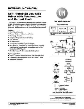
ncv8406.pdf
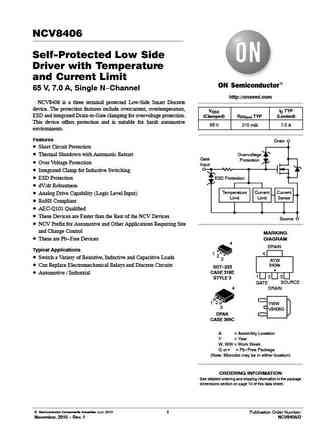
NCV8406 Self-Protected Low Side Driver with Temperature and Current Limit 65 V, 7.0 A, Single N-Channel http //onsemi.com NCV8406 is a three terminal protected Low-Side Smart Discrete device. The protection features include overcurrent, overtemperature, VDSS ID TYP ESD and integrated Drain-to-Gate clamping for overvoltage protection. (Clamped) RDS(on) TYP (Limited) This device offers
ncv8408.pdf
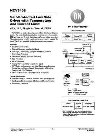
NCV8408 Self-Protected Low Side Driver with Temperature and Current Limit 42 V, 10 A, Single N-Channel, DPAK http //onsemi.com NCV8408 is a single channel protected Low-Side Smart Discrete VDSS ID MAX device. The protection features include overcurrent, overtemperature, RDS(on) TYP (Clamped) (Limited) ESD and integrated Drain-to-Gate clamping for overvoltage protection. Thermal prot
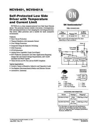
ncv8403a.pdf
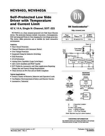
NCV8403, NCV8403A Self-Protected Low Side Driver with Temperature and Current Limit 42 V, 14 A, Single N-Channel, SOT-223 http //onsemi.com NCV8403/A is a three terminal protected Low-Side Smart Discrete VDSS ID MAX device. The protection features include overcurrent, overtemperature, RDS(on) TYP (Clamped) (Limited) ESD and integrated Drain-to-Gate clamping for overvoltage protection
ncv8406a.pdf
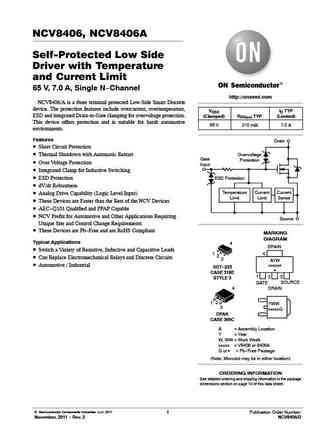
NCV8406, NCV8406A Self-Protected Low Side Driver with Temperature and Current Limit 65 V, 7.0 A, Single N-Channel http //onsemi.com NCV8406/A is a three terminal protected Low-Side Smart Discrete device. The protection features include overcurrent, overtemperature, VDSS ID TYP ESD and integrated Drain-to-Gate clamping for overvoltage protection. (Clamped) RDS(on) TYP (Limited) This d
ncv8401a ncv8401adtrkg ncv8401dtrkg.pdf
NCV8401, NCV8401A Self-Protected Low Side Driver with Temperature and Current Limit NCV8401/A is a three terminal protected Low-Side Smart Discrete device. The protection features include overcurrent, overtemperature, http //onsemi.com ESD and integrated Drain-to-Gate clamping for overvoltage protection. This device offers protection and is suitable for harsh automotive VDSS ID MAX (C
nvmfd6h840nl.pdf
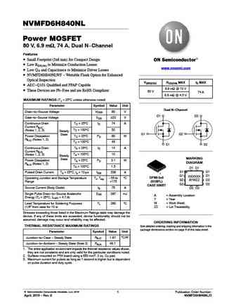
NVMFD6H840NL Power MOSFET 80 V, 6.9 mW, 74 A, Dual N-Channel Features Small Footprint (5x6 mm) for Compact Design Low RDS(on) to Minimize Conduction Losses www.onsemi.com Low QG and Capacitance to Minimize Driver Losses NVMFD6H840NLWF - Wettable Flank Option for Enhanced Optical Inspection V(BR)DSS RDS(ON) MAX ID MAX AEC-Q101 Qualified and PPAP Capable 6.9 mW @ 1
ncv8403.pdf
NCV8403 Self-Protected Low Side Driver with Temperature and Current Limit 42 V, 14 A, Single N-Channel, SOT-223 http //onsemi.com NCV8403 is a three terminal protected Low-Side Smart Discrete VDSS ID MAX device. The protection features include overcurrent, overtemperature, RDS(on) TYP (Clamped) (Limited) ESD and integrated Drain-to-Gate clamping for overvoltage protection. This devi
ncv8402ad.pdf
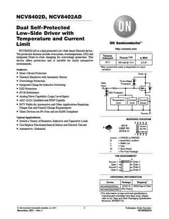
NCV8402D, NCV8402AD Dual Self-Protected Low-Side Driver with Temperature and Current Limit http //onsemi.com NCV8402D/AD is a dual protected Low-Side Smart Discrete device. The protection features include overcurrent, overtemperature, ESD and V(BR)DSS integrated Drain-to-Gate clamping for overvoltage protection. This RDS(ON) TYP ID MAX (Clamped) device offers protection and is suita
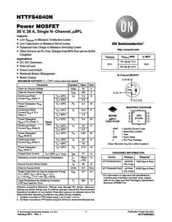
nttfs4840n.pdf
NTTFS4840N Power MOSFET 30 V, 26 A, Single N-Channel, m8FL Features Low RDS(on) to Minimize Conduction Losses Low Capacitance to Minimize Driver Losses Optimized Gate Charge to Minimize Switching Losses http //onsemi.com These Devices are Pb-Free, Halogen Free/BFR Free and are RoHS Compliant V(BR)DSS RDS(on) MAX ID MAX Applications 24 mW @ 10 V DC-DC Converters
ntmd4840n.pdf
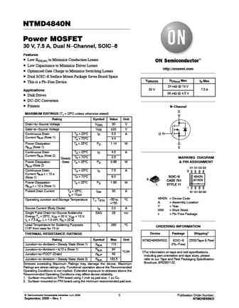
NTMD4840N Power MOSFET 30 V, 7.5 A, Dual N-Channel, SOIC-8 Features Low RDS(on) to Minimize Conduction Losses Low Capacitance to Minimize Driver Losses http //onsemi.com Optimized Gate Charge to Minimize Switching Losses Dual SOIC-8 Surface Mount Package Saves Board Space V(BR)DSS RDS(on) Max ID Max This is a Pb-Free Device 24 mW @ 10 V 30 V 7.5 A Applications
ncv8402d.pdf
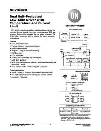
NCV8402D Dual Self-Protected Low-Side Driver with Temperature and Current Limit http //onsemi.com NCV8402D is a dual protected Low-Side Smart Discrete device. The protection features include overcurrent, overtemperature, ESD and V(BR)DSS integrated Drain-to-Gate clamping for overvoltage protection. This RDS(ON) TYP ID MAX (Clamped) device offers protection and is suitable for harsh
ncv8405a.pdf
NCV8405, NCV8405A Self-Protected Low Side Driver with Temperature and Current Limit NCV8405/A is a three terminal protected Low-Side Smart Discrete device. The protection features include overcurrent, overtemperature, http //onsemi.com ESD and integrated Drain-to-Gate clamping for overvoltage protection. This device is suitable for harsh automotive environments. V(BR)DSS RDS(ON) TYP
ncv8405.pdf

NCV8405 Self-Protected Low Side Driver with Temperature and Current Limit NCV8405 is a three terminal protected Low-Side Smart Discrete device. The protection features include overcurrent, overtemperature, http //onsemi.com ESD and integrated Drain-to-Gate clamping for overvoltage protection. This device is suitable for harsh automotive environments. V(BR)DSS RDS(ON) TYP ID MAX (Cla
ncv8403a ncv8403b.pdf
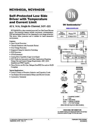
NCV8403A, NCV8403B Self-Protected Low Side Driver with Temperature and Current Limit 42 V, 14 A, Single N-Channel, SOT-223 www.onsemi.com NCV8403A/B is a three terminal protected Low-Side Smart Discrete VDSS ID MAX device. The protection features include overcurrent, overtemperature, RDS(on) TYP (Clamped) (Limited) ESD and integrated Drain-to-Gate clamping for overvoltage protection.
sk840303.pdf
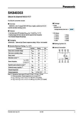
This product complies with the RoHS Directive (EU 2002/95/EC). SK840303 Silicon N-channel MOS FET For DC-DC converter circuits Package Overview Code SK840303 is the N-channel MOS FET that is highly suitable for DC-DC HSSO8-F1-B converter and other switching circuits. Package dimension clicks here. Click! Features Low drain-source ON resistance RDS(on) typ
sk840317.pdf

Doc No. TT4-EA-14209 Revision. 5 Product Standards MOS FET SK8403170L SK8403170L Silicon N-channel MOS FET Unit mm 3.25 For Load-switching / For DC-DC Converter 3.05 0.22 8 7 6 5 Features Low Drain-source On-state Resistance RDS(on) typ = 3.9 m (VGS = 4.5 V) Halogen-free / RoHS compliant (EU RoHS / UL-94 V-0 / MSL Level 1 compliant) 1 2 3 4 0.3 1.0
sk840320.pdf
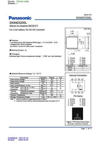
Doc No. TT4-EA-14682 Revision. 1 Product Standard MOS FET SK8403200L SK8403200L Silicon N-channel MOSFET Unit mm For Li-ion battery / for DC-DC converter 3.25 3.05 0.22 8 7 6 5 Features Low drain-source ON resistance RDS(on)typ. = 3.7 m (VGS = 10 V) Halogen-free / RoHS compliant (EU RoHS / UL-94 V-0 / MSL Level 1 compliant) 1 2 3 4 Marking Symbol 1A 0.3
2sc5840.pdf
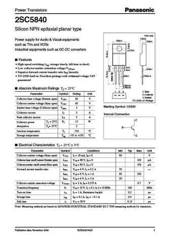
Power Transistors 2SC5840 Silicon NPN epitaxial planar type Unit mm 4.6 0.2 Power supply for Audio & Visual equipments 9.9 0.3 2.9 0.2 such as TVs and VCRs Industrial equipments such as DC-DC converters 3.2 0.1 Features High-speed switching (tstg storage time/tf fall time is short) 1.4 0.2 Low collector-emitter saturation voltage VCE(sat) 2.6 0.1 1.6 0.2
sk840318.pdf
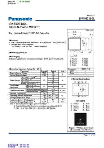
Doc No. TT4-EA-14486 Revision. 2 Product Standards MOS FET SK8403180L SK8403180L Silicon N-channel MOS FET Unit mm 3.25 For Load-switching / For DC-DC Converter 3.05 0.22 8 7 6 5 Features Low Drain-source On-state Resistance RDS(on) typ = 6.7 m (VGS = 4.5 V) Halogen-free / RoHS compliant (EU RoHS / UL-94 V-0 / MSL Level 1 compliant) 1 2 3 4 0.3 1.0
sk840319.pdf

Doc No. TT4-EA-14210 Revision. 6 Product Standards MOS FET SK8403190L SK8403190L Silicon N-channel MOS FET Unit mm 3.25 For Load-switching / For DC-DC Converter 3.05 0.22 8 7 6 5 Features Low Drain-source On-state Resistance RDS(on) typ = 10 m (VGS = 4.5 V) Halogen-free / RoHS compliant (EU RoHS / UL-94 V-0 / MSL Level 1 compliant) 1 2 3 4 0.3 1.0 Ma
sk840316.pdf

Doc No. TT4-EA-14485 Revision. 2 Product Standards MOS FET SK8403160L SK8403160L Silicon N-channel MOS FET Unit mm 3.25 For Load-switching / For DC-DC Converter 3.05 0.22 8 7 6 5 Features Low Drain-source On-state Resistance RDS(on) typ = 3.2 m (VGS = 4.5 V) Halogen-free / RoHS compliant (EU RoHS / UL-94 V-0 / MSL Level 1 compliant) 1 2 3 4 0.3 1.0
uf840kl-ta3-r uf840kg-ta3-r uf840kl-tf3-r uf840kg-tf3-r uf840kl-tf1-t uf840kg-tf1-t uf840kl-tn3-r uf840kg-tn3-r uf840kl-tq2-t uf840kg-tq2-t uf840kl-tq2-r uf840kg-tq2-r.pdf
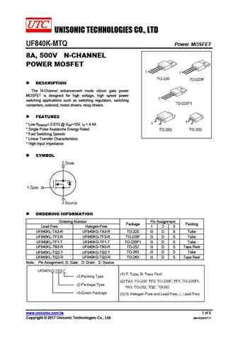
UNISONIC TECHNOLOGIES CO., LTD UF840K-MTQ Power MOSFET 8A, 500V N-CHANNEL POWER MOSFET DESCRIPTION The N-Channel enhancement mode silicon gate power MOSFET is designed for high voltage, high speed power switching applications such as switching regulators, switching converters, solenoid, motor drivers, relay drivers. FEATURES * Low RDS(ON)
uf840.pdf
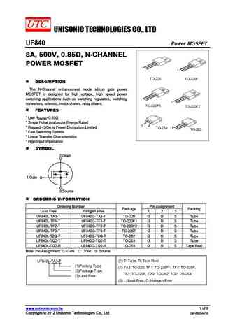
UNISONIC TECHNOLOGIES CO., LTD UF840 Power MOSFET 8A, 500V, 0.85 , N-CHANNEL POWER MOSFET DESCRIPTION The N-Channel enhancement mode silicon gate power MOSFET is designed for high voltage, high speed power switching applications such as switching regulators, switching converters, solenoid, motor drivers, relay drivers. FEATURES * Low RDS(ON)=0.85 * Single Pulse Ava
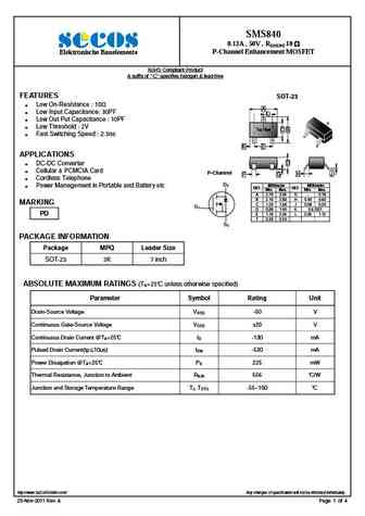
sms840.pdf
SMS840 0.13A , 50V , RDS(ON) 10 P-Channel Enhancement MOSFET Elektronische Bauelemente RoHS Compliant Product A suffix of -C specifies halogen & lead-free FEATURES SOT-23 Low On-Resistance 10 A Low Input Capacitance 30PF L 3 Low Out Put Capacitance 10PF 3 Low Threshold 2V Top View C B Fast Switching Speed 2.5ns 1 1 2 2
bf840 bf841.pdf
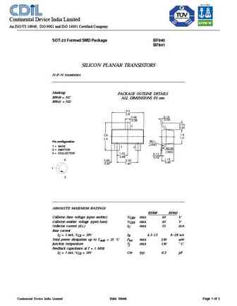
Continental Device India Limited An ISO/TS 16949, ISO 9001 and ISO 14001 Certified Company SOT-23 Formed SMD Package BF840 BF841 SILICON PLANAR TRANSISTORS N P N transistors Marking PACKAGE OUTLINE DETAILS BF840 = NC ALL DIMENSIONS IN mm BF841 = ND Pin configuration 1 = BASE 2 = EMITTER 3 = COLLECTOR 3 1 2 ABSOLUTE MAXIMUM RATINGS BF840 BF841 Collector base voltage (op
dg840.pdf
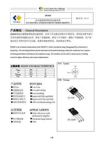
DG840 V1.0 N N-CHANNE ENHANCEMENT MODE MOSFET General Description DG840 N
cjde8404.pdf
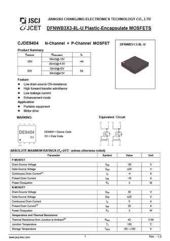
JIANGSU CHANGJING ELECTRONICS TECHNOLOGY CO., LTD DFNWB3X3-8L-U Plastic-Encapsulate MOSFETS CJDE8404 N-Channel + P-Channel MOSFET DFNWB3 3-8L-U Product Summary V R I (BR)DSS DS(on)MAX D 50m @-10V -30V -4A 80m @-4.5V 50m @10V 30V 5A 80m @4.5V Feature Low drain-source ON-resistance High forward transfer admittance Low leakage current Enhancement mo
2n5838 2n5839 2n5840.pdf
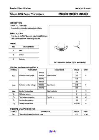
Product Specification www.jmnic.com Silicon NPN Power Transistors 2N5838 2N5839 2N5840 DESCRIPTION With TO-3 package Low collector-emitter saturation voltage APPLICATIONS For use in switching power supply applications and other inductive switching circuits. PINNING PIN DESCRIPTION 1 Base 2 Emitter 3 Collector Fig.1 simplified outline (TO-3) and symbol Absolute max
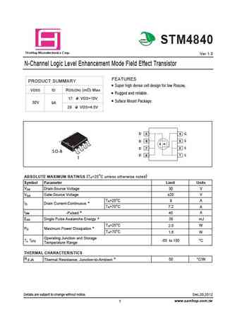
cep840a ceb840a cef840a.pdf
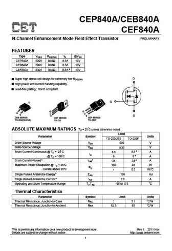
CEP840A/CEB840A CEF840A PRELIMINARY N-Channel Enhancement Mode Field Effect Transistor FEATURES Type VDSS RDS(ON) ID @VGS CEP840A 500V 0.85 8.5A 10V CEB840A 500V 0.85 8.5A 10V CEF840A 500V 0.85 8.5A d 10V D Super high dense cell design for extremely low RDS(ON). High power and current handing capability. Lead-free plating ; RoHS compliant. G S CEB SERIES CEP SERIES CEF
cep840l ceb840l cef840l.pdf
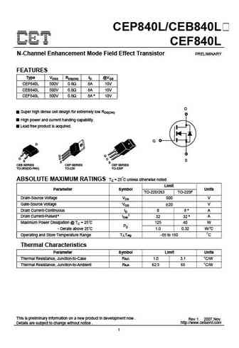
CEP840L/CEB840L CEF840L N-Channel Enhancement Mode Field Effect Transistor PRELIMINARY FEATURES Type VDSS RDS(ON) ID @VGS CEP840L 500V 0.8 8A 10V CEB840L 500V 0.8 8A 10V CEF840L 500V 0.8 8A e 10V D Super high dense cell design for extremely low RDS(ON). High power and current handing capability. Lead free product is acquired. G S CEB SERIES CEP SERIES CEF SERIES TO-263(
cep840g ceb840g cef840g.pdf
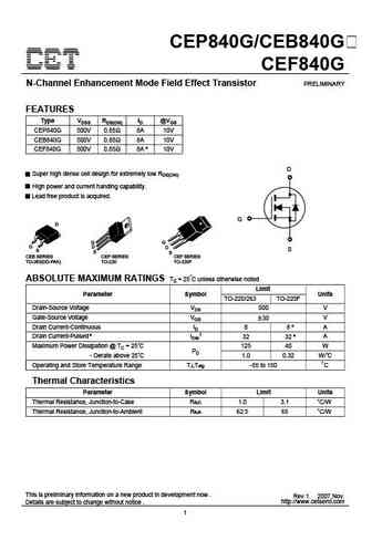
CEP840G/CEB840G CEF840G N-Channel Enhancement Mode Field Effect Transistor PRELIMINARY FEATURES Type VDSS RDS(ON) ID @VGS CEP840G 500V 0.85 8A 10V CEB840G 500V 0.85 8A 10V CEF840G 500V 0.85 8A e 10V D Super high dense cell design for extremely low RDS(ON). High power and current handing capability. Lead free product is acquired. G S CEB SERIES CEP SERIES CEF SERIES TO-2
ceu840a ced840a.pdf
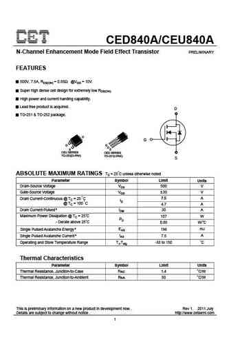
CED840A/CEU840A N-Channel Enhancement Mode Field Effect Transistor PRELIMINARY FEATURES 500V, 7.5A, RDS(ON) = 0.85 @VGS = 10V. Super high dense cell design for extremely low RDS(ON). High power and current handing capability. Lead free product is acquired. D TO-251 & TO-252 package. D G G S CEU SERIES CED SERIES TO-252(D-PAK) TO-251(I-PAK) S ABSOLUTE MAXIMUM RATINGS Tc = 25
hirf840.pdf
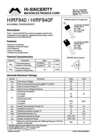
Spec. No. MOS200505 HI-SINCERITY Issued Date 2005.06.01 Revised Date 2005.06.08 MICROELECTRONICS CORP. Page No. 1/4 HIRF840 Series Pin Assignment HIRF840 / HIRF840F Tab N-CHANNEL POWER MOSFET 3-Lead Plastic TO-220AB Package Code E Pin 1 Gate Pin 2 & Tab Drain Description Pin 3 Source This N - Channel MOSFETs provide the designer with the best combination of fast swi
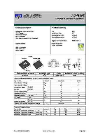
ao4840.pdf
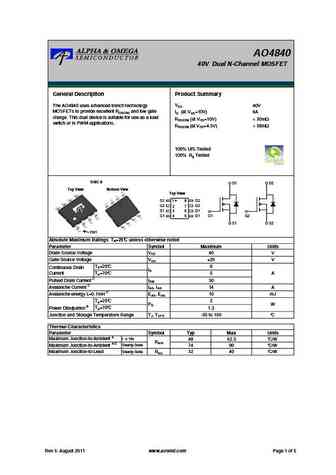
AO4840 40V Dual N-Channel MOSFET General Description Product Summary VDS 40V The AO4840 uses advanced trench technology MOSFETs to provide excellent RDS(ON) and low gate ID (at VGS=10V) 6A charge. This dual device is suitable for use as a load RDS(ON) (at VGS=10V)
ao4840e.pdf
AO4840E 40V Dual N-Channel AlphaMOS General Description Product Summary VDS Advanced trench technology 40V Low RDS(ON) ID (at VGS=10V) 6A Low Gate Charge RDS(ON) (at VGS=10V)
irf840.pdf
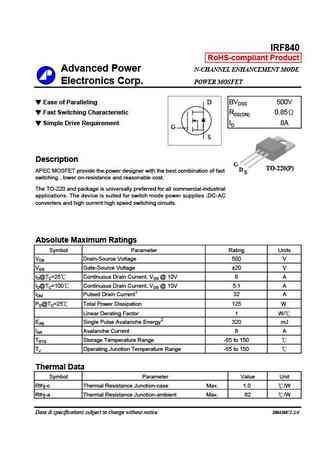
IRF840 RoHS-compliant Product Advanced Power N-CHANNEL ENHANCEMENT MODE Electronics Corp. POWER MOSFET Ease of Paralleling D BVDSS 500V Fast Switching Characteristic RDS(ON) 0.85 Simple Drive Requirement ID 8A G S Description G TO-220(P) D APEC MOSFET provide the power designer with the best combination of fast S switching , lower on-resistance and reasonable cost.
irf840s.pdf
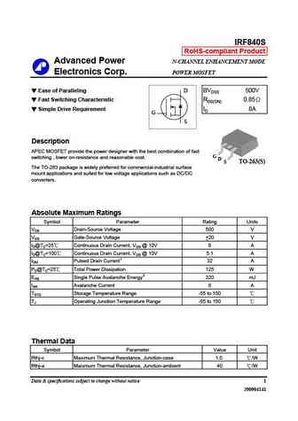
IRF840S RoHS-compliant Product Advanced Power N-CHANNEL ENHANCEMENT MODE Electronics Corp. POWER MOSFET Ease of Paralleling D BVDSS 500V Fast Switching Characteristic RDS(ON) 0.85 Simple Drive Requirement ID 8A G S Description APEC MOSFET provide the power designer with the best combination of fast G switching , lower on-resistance and reasonable cost. D S TO-263(S)
irf840i.pdf
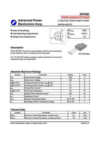
IRF840I RoHS-compliant Product Advanced Power N-CHANNEL ENHANCEMENT MODE Electronics Corp. POWER MOSFET Ease of Paralleling D BVDSS 500V Fast Switching Characteristic RDS(ON) 0.85 Simple Drive Requirement ID 8A G S Description APEC MOSFET provide the power designer with the best combination G of fast switching , lower on-resistance and reasonable D TO-220CFM(I) S T
am4840n.pdf
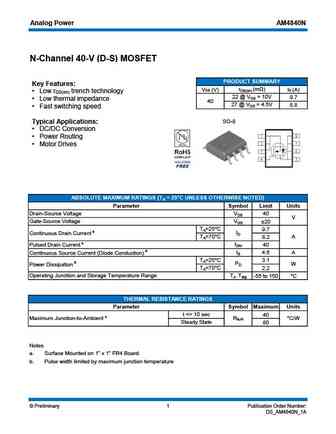
Analog Power AM4840N N-Channel 40-V (D-S) MOSFET PRODUCT SUMMARY Key Features rDS(on) (m ) VDS (V) ID (A) Low r trench technology DS(on) 22 @ VGS = 10V 9.7 Low thermal impedance 40 27 @ VGS = 4.5V 8.8 Fast switching speed Typical Applications SO-8 DC/DC Conversion Power Routing Motor Drives ABSOLUTE MAXIMUM RATINGS (TA = 25 C UNLESS OTHERWI
mtc8402s6r.pdf
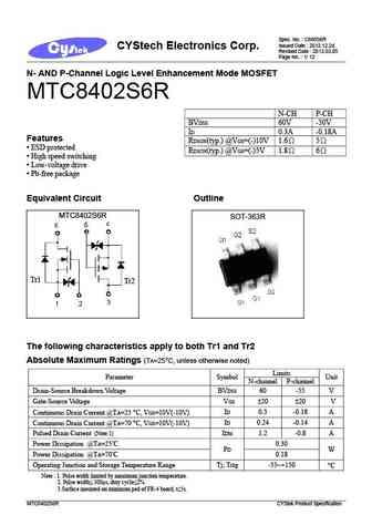
Spec. No. C888S6R Issued Date 2012.12.24 CYStech Electronics Corp. Revised Date 2013.03.05 Page No. 1/ 12 N- AND P-Channel Logic Level Enhancement Mode MOSFET MTC8402S6R N-CH P-CH BVDSS 60V -50V ID 0.3A -0.18A Features RDSON(typ.) @VGS=(-)10V 1.6 5 ESD protected RDSON(typ.) @VGS=(-)5V 1.8 6 High speed switching Low-voltage drive Pb-fr
mtc8404v8.pdf
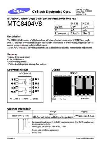
Spec. No. C914V8 Issued Date 2013.09.30 CYStech Electronics Corp. Revised Date Page No. 1/12 N- AND P-Channel Logic Level Enhancement Mode MOSFET N-CH P-CH MTC8404V8 BVDSS 30V -30V ID 6A -6A RDSON(MAX.) 23m 28m Description The MTC8404V8 consists of a N-channel and a P-channel enhancement-mode MOSFET in a single DFN3 3 package, providing the designer with t
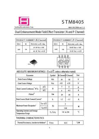
stm8405.pdf
S TM8405 S amHop Microelectronics C orp. MAY .04,2006 ver 1.5 Dual Enhancement Mode Field Effect Transistor ( N and P Channel) (N-C hannel) (P PR ODUC T S UMMAR Y PR ODUC T S UMMAR Y -C hannel) VDS S ID R DS (ON) ( m ) Max VDS S ID R DS (ON) ( m ) Max 25 @ VGS =10V 50 @ VGS =-10V -30V -5A 30V 7A 40 @ VGS =4.5V 70 @ VGS =-4.5V D1 D1 D2 D2 8 7 6 5 SO-8 1 1 2 3 4 S 1 G 1 S
stm8401.pdf
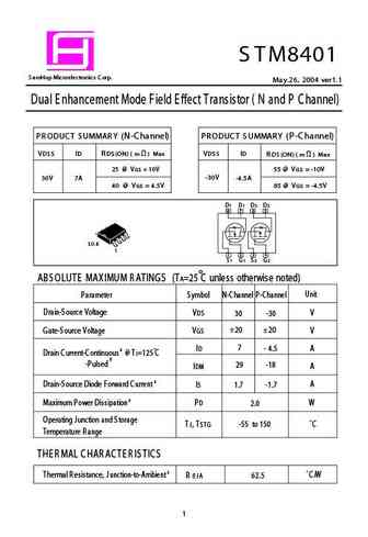
S T M8401 S amHop Microelectronics C orp. May.26, 2004 ver1.1 Dual E nhancement Mode Field E ffect Transistor ( N and P Channel) (N-C hannel) (P P R ODUC T S UMMAR Y P R ODUC T S UMMAR Y -C hannel) V DS S ID R DS (ON) ( m W ) Max V DS S ID R DS (ON) ( m W ) Max 25 @ VG S = 10V 55 @ V G S = -10V -30V -4.5A 7A 30V 40 @ V G S = 4.5V 85 @ V G S = -4.5V D1 D1 D2 D2 8 7 6 5 S O-8 1
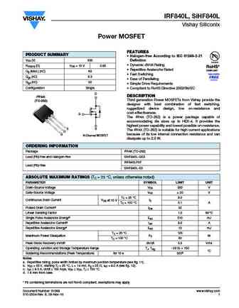
irfs840.pdf
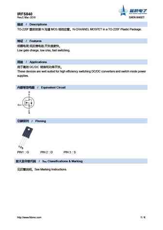
IRFS840 Rev.E Mar.-2016 DATA SHEET / Descriptions TO-220F N MOS N-CHANNEL MOSFET in a TO-220F Plastic Package. / Features , , Low gate charge, low crss, fast switching. / Applications DC/DC These devices are well suited for high efficiency
brd840.pdf
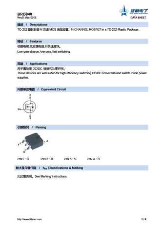
BRD840 Rev.D May.-2016 DATA SHEET / Descriptions TO-252 N MOS N-CHANNEL MOSFET in a TO-252 Plastic Package. / Features , , Low gate charge, low crss, fast switching. / Applications DC/DC These devices are well suited for high efficiency
irf840.pdf
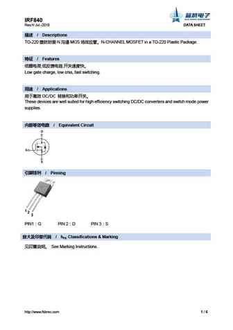
IRF840 Rev.H Jul.-2018 DATA SHEET / Descriptions TO-220 N MOS N-CHANNEL MOSFET in a TO-220 Plastic Package. / Features , , Low gate charge, low crss, fast switching. / Applications DC/DC These devices are well suited for high efficiency swi
brb840.pdf
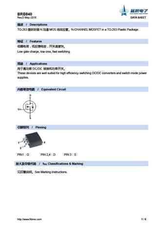
BRB840 Rev.D May.-2016 DATA SHEET / Descriptions TO-263 N MOS N-CHANNEL MOSFET in a TO-263 Plastic Package. / Features Low gate charge, low crss, fast switching. / Applications DC/DC These devices are well suited for high efficie
hfp840.pdf
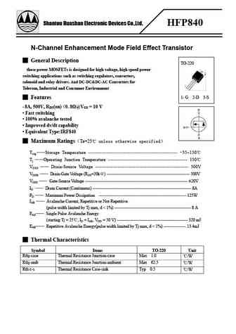
Shantou Huashan Electronic Devices Co.,Ltd. HFP840 N-Channel Enhancement Mode Field Effect Transistor General Description TO-220 these power MOSFETs is designed for high voltage, high speed power switching applications such as switching regulators, converters, solenoid and relay drivers. And DC-DC&DC-AC Converters for Telecom, Industrial and Consumer Environment 1- G 2-D
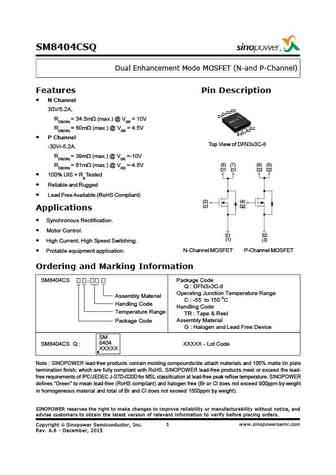
sm8401csq.pdf
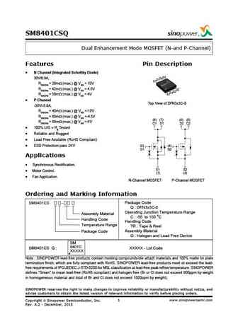
SM8401CSQ Dual Enhancement Mode MOSFET (N-and P-Channel) Features Pin Description N Channel (Integrated Schottky Diode) D2 30V/6.9A, D1D2 D1 RDS(ON) = 29m (max.) @ VGS = 10V RDS(ON) = 42m (max.) @ VGS = 4.5V G2 S2 S1G1 RDS(ON) = 50m (max.) @ VGS = 4V P Channel Top View of DFN3x3C-8 -30V/-5.9A, RDS(ON) = 40m (max.) @ VGS =-10V RDS(ON) = 60m (max.) @ VGS =-4.5V (8) (7) (
sm8403csq.pdf
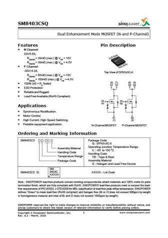
SM8403CSQ Dual Enhancement Mode MOSFET (N-and P-Channel) Features Pin Description N Channel 30V/5.6A, D2 D1D2 RDS(ON) = 29m (max.) @ VGS = 10V D1 RDS(ON) = 39m (max.) @ VGS = 4.5V G2 S2 P Channel S1G1 -30V/-4.2A, Top View of DFN3x3C-8 RDS(ON) = 63m (max.) @ VGS =-10V RDS(ON) = 100m (max.) @ VGS =-4.5V (8) (7) (6) (5) 100% UIS + Rg Tested D1 D1 D2 D2 ESD Protection
sm4840nsk.pdf
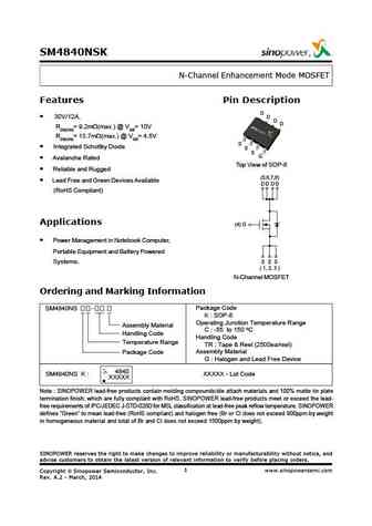
SM4840NSK N-Channel Enhancement Mode MOSFET Features Pin Description D D 30V/12A, D D RDS(ON)= 9.2m (max.) @ VGS= 10V RDS(ON)= 13.7m (max.) @ VGS= 4.5V S Integrated Schottky Diode S S G Avalanche Rated Top View of SOP-8 Reliable and Rugged (5,6,7,8) Lead Free and Green Devices Available D D DD (RoHS Compliant) Applications (4) G Power Management in Notebook
sm8404csqa.pdf
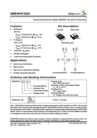
SM8404CSQA Dual Enhancement Mode MOSFET (N-and P-Channel) Features Pin Description N Channel Top View Bottom View 30V/11A, D2 D1D2 RDS(ON) = 34.5m (max.) @ VGS = 10V D1 RDS(ON) = 60m (max.) @ VGS = 4.5V G2 Pin 1 S2 P Channel S1G1 -30V/-13.3A, DFN3x3B-8_EP2 RDS(ON) = 39m (max.) @ VGS =-10V RDS(ON) = 61m (max.) @ VGS =-4.5V (8) (7) (6) (5) D1 D1 D2 D2 100% UIS + Rg T
sm8404csq.pdf
SM8404CSQ Dual Enhancement Mode MOSFET (N-and P-Channel) Features Pin Description N Channel 30V/5.2A, D2 D1D2 D1 RDS(ON) = 34.5m (max.) @ VGS = 10V RDS(ON) = 60m (max.) @ VGS = 4.5V G2 S2 S1G1 P Channel Top View of DFN3x3C-8 -30V/-5.2A, RDS(ON) = 39m (max.) @ VGS =-10V (8) (7) (6) (5) RDS(ON) = 61m (max.) @ VGS =-4.5V D1 D1 D2 D2 100% UIS + Rg Tested Reliable and Ru
cs840f a9h.pdf
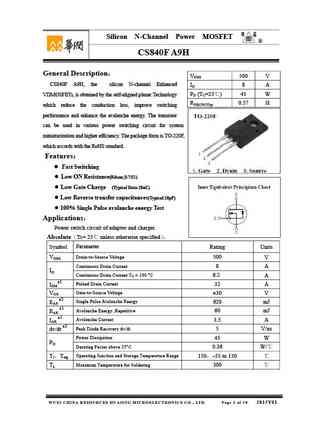
Silicon N-Channel Power MOSFET R CS840F A9H General Description VDSS 500 V CS840F A9H, the silicon N-channel Enhanced ID 8 A PD (TC=25 ) 45 W VDMOSFETs, is obtained by the self-aligned planar Technology RDS(ON)Typ 0.57 which reduce the conduction loss, improve switching performance and enhance the avalanche energy. The transistor can be used in various pow
cs840 a8h.pdf

Silicon N-Channel Power MOSFET R CS840 A8H General Description VDSS 500 V CS840 A8H, the silicon N-channel Enhanced VDMOSFETs, ID 8 A PD (TC=25 ) 110 W is obtained by the self-aligned planar Technology which reduce RDS(ON)Typ 0.57 the conduction loss, improve switching performance and enhance the avalanche energy. The transistor can be used in various power s
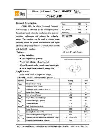
cs840 a8d.pdf
Silicon N-Channel Power MOSFET R CS840 A8D General Description VDSS 500 V CS840 A8D, the silicon N-channel Enhanced ID 7 A PD(TC=25 ) 100 W VDMOSFETs, is obtained by the self-aligned planar RDS(ON)Typ 0.68 Technology which reduce the conduction loss, improve switching performance and enhance the avalanche energy. The transistor can be used in various power
cs840f a9d.pdf

Silicon N-Channel Power MOSFET R CS840F A9D General Description VDSS 500 V CS840F A9D, the silicon N-channel Enhanced ID 7 A PD(TC=25 ) 35 W VDMOSFETs, is obtained by the self-aligned planar Technology RDS(ON)Typ 0.68 which reduce the conduction loss, improve switching performance and enhance the avalanche energy. The transistor can be used in various powe
bu8403.pdf
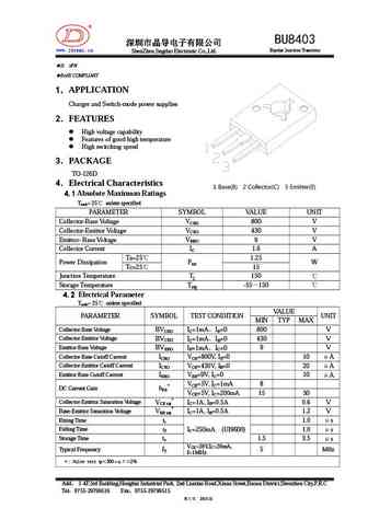
R BU8403 www.jdsemi.cn Bipolar Junction Transistor ShenZhen Jingdao Electronic Co.,Ltd. Si NPN RoHS COMPLIANT 1 1 1 APPLICATION 1 Charger and Switch-mode power supplies 2 2 2 FEATURES 2 High voltage capab
ftk840 ftk840p f.pdf
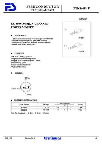
SEMICONDUCTOR FTK840P / F TECHNICAL DATA MOSFET 8A, 500V, 0.85 , N-CHANNEL POWER MOSFET P 1 DESCRIPTION TO-220 The N-Channel enhancement mode silicon gate power MOSFET is designed for high voltage, high speed power switching applications such as switching regulators, switching converters, solenoid, motor drivers, relay drivers. F 1 TO-220F FEATURES * 8A, 500V, Low RDS(ON
tpcp8404.pdf
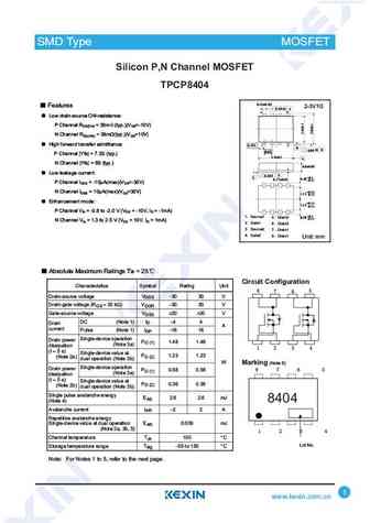
SMD Type MOSFET Transistors Silicon P,N Channel MOSFET TPCP8404 0.33 0.05 Features 2-3V1G 0.05 M A 8 5 Low drain-source ON-resistance P Channel RDS(ON) = 38m (typ.)(VGS=-10V) N Channel RDS(ON) = 38m (typ.)(VGS=10V) High forward transfer admittance 0.475 1 4 B 0.05 M B 0.65 P Channel Yfs = 7.3S (typ.) 2.9 0.1 A N Channel Yfs = 8S (typ.) 0.8 0.05 Low leakage curr
kpcf8402.pdf
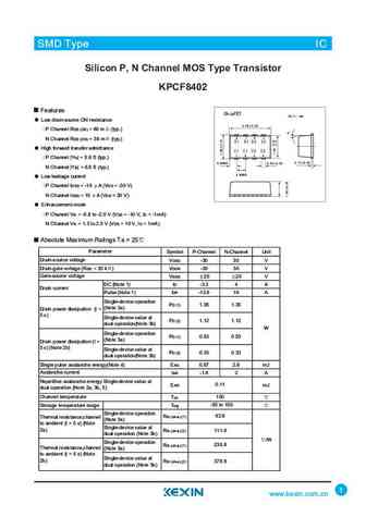
SMD Type IC SMD Type IC Silicon P, N Channel MOS Type Transistor KPCF8402 Features Low drain-source ON resistance P Channel RDS (ON) =60m (typ.) N Channel RDS (ON) =38 m (typ.) High forward transfer admittance P Channel Yfs =5.9S(typ.) N Channel Yfs =6.8S(typ.) Low leakage current P Channel IDSS =-10 A(VDS =-30 V) N Channel IDSS =10 A(VDS =30 V) Enhancement-mode P Cha
irf840s.pdf
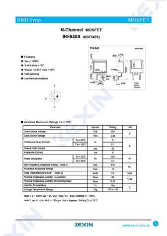
SMD Type MOSFET N-Channel MOSFET IRF840S (KRF840S) Features VDS (V) =500V ID =8 A (VGS = 10V) RDS(ON) 0.85 (VGS = 10V) Fast switching Low thermal resistance d g s Absolute Maximum Ratings Ta = 25 Parameter Symbol Rating Unit Drain-Source Voltage VDS 500 V Gate-Source Voltage VGS 20 Ta = 25 8 Continuous Drain Current ID Ta = 1
ao4840.pdf
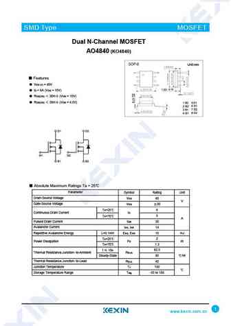
SMD Type MOSFET Dual N-Channel MOSFET AO4840 (KO4840) SOP-8 Unit mm Features VDS (V) = 40V 1.50 0.15 ID = 6A (VGS = 10V) RDS(ON) 30m (VGS = 10V) RDS(ON) 38m (VGS = 4.5V) 1 S2 5 D1 6 D1 2 G2 7 D2 3 S1 8 D2 4 G1 D1 D2 G1 G2 S1 S2 Absolute Maximum Ratings Ta = 25 Parameter Symbol Rating Unit Drain-Source Voltage VDS 40 V Gate-So
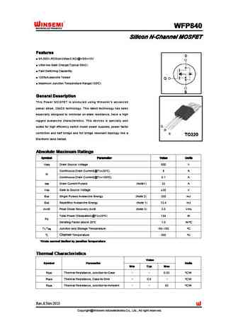
wff840.pdf
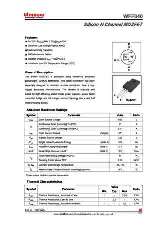
WFF840 WFF840 WFF840 WFF840 Silicon N-Channel MOSFET Silicon N-Channel MOSFET Silicon N-Channel MOSFET Silicon N-Channel MOSFET Features Features Features Features 8A,500V,RDS(on)(Max 0.8 )@VGS=10V Ultra-low Gate Charge(Typical 48nC) Fast Switching Capability 100%Avalanche Tested Isolation Voltage ( VISO = 4000V AC ) Maximum Junction Temperature Range(15
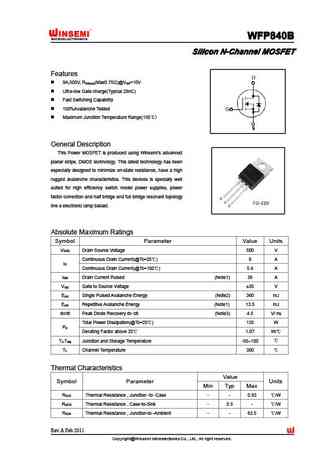
wff840b.pdf
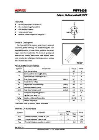
WFF840B WFF840B WFF840B WFF840B Silicon N-Channel MOSFET Silicon N-Channel MOSFET Silicon N-Channel MOSFET Silicon N-Channel MOSFET Features 9A,500V, R (Max0.75 )@V =10V DS(on) GS Ultra-low Gate charge(Typical 28nC) Fast Switching Capability 100%Avalanche Tested Maximum Junction Temperature Range(150 ) General Description This Power MOSFET is produced usi
wfp840.pdf
WFP840 WFP840 WFP840 WFP840 Silicon N-Channel MOSFET Silicon N-Channel MOSFET Silicon N-Channel MOSFET Silicon N-Channel MOSFET Features Features Features Features 8A,500V,RDS(on)(Max 0.8 )@VGS=10V Ultra-low Gate Charge(Typical 59nC) Fast Switching Capability 100%Avalanche Tested Maximum Junction Temperature Range(150 ) General Description General Descri
wfp840b.pdf
WFP840B WFP840B WFP840B WFP840B Silicon N-Channel MOSFET Silicon N-Channel MOSFET Silicon N-Channel MOSFET Silicon N-Channel MOSFET Features 9A,500V, R (Max0.75 )@V =10V DS(on) GS Ultra-low Gate charge(Typical 28nC) Fast Switching Capability 100%Avalanche Tested Maximum Junction Temperature Range(150 ) General Description This Power MOSFET is produced usi
pje8404.pdf
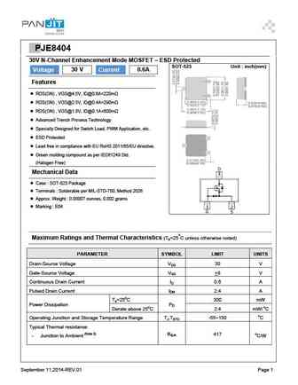
PPJE8404 30V N-Channel Enhancement Mode MOSFET ESD Protected SOT-523 Unit inch(mm) 30 V 0.6A Voltage Current Features RDS(ON) , VGS@4,5V, ID@0.6A
bss8402dw.pdf
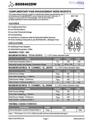
BSS8402DW COMPLIMENTARY PAIR ENHANCEMENT MODE MOSFETS This space-efficient device contains an electrically-isolated complimentary pair of enhancement-mode MOSFETs (one N-channel and one P-channel). It SOT- 363 comes in a very small SOT-363 package. This device is ideal for portable applications where board space is at a premium. 4 4 FEATURES 5 5 Complimentary Pairs 6 6 3 3 Low O
pje8402.pdf

PPJE8402 20V N-Channel Enhancement Mode MOSFET ESD Protected SOT-523 Unit inch(mm) 20 V 0.7A Voltage Current Features RDS(ON) , VGS@4,5V, ID@0.7A
pje8406.pdf
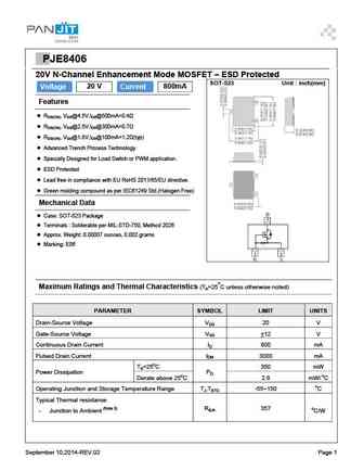
PPJE8406 20V N-Channel Enhancement Mode MOSFET ESD Protected SOT-523 Unit inch(mm) 20 V 800mA Voltage Current Features RDS(ON), VGS@4.5V,IDS@500mA=0.4 RDS(ON), VGS@2.5V,IDS@300mA=0.7 RDS(ON), VGS@1.8V,IDS@100mA=1.2 (typ) Advanced Trench Process Technology Specially Designed for Load Switch or PWM application. ESD Protected Lead f
pje8400.pdf
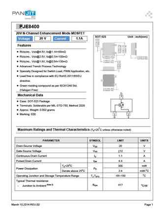
PPJE8400 20V N-Channel Enhancement Mode MOSFET SOT-523 Unit inch(mm) 20 V 1.1A Voltage Current Features RDS(ON) , VGS@4.5V, ID@1.1A
pje8401.pdf
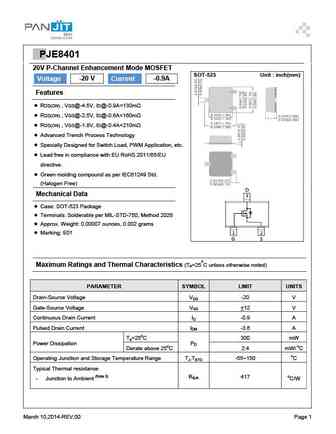
PPJE8401 20V P-Channel Enhancement Mode MOSFET SOT-523 Unit inch(mm) Voltage -20 V Current -0.9A Features RDS(ON) , VGS@-4.5V, ID@-0.9A

blv840.pdf
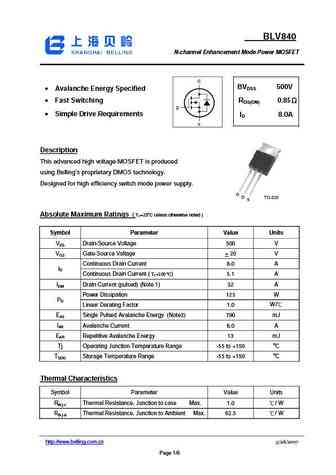
BLV840 N-channel Enhancement Mode Power MOSFET 500V DSS Avalanche Energy Specified BV Fast Switching RDS(ON) 0.85 Simple Drive Requirements ID 8.0A Description This advanced high voltage MOSFET is produced using Belling s proprietary DMOS technology. Designed for high efficiency switch mode power supply. Absolute Maximum Ratings ( TC=25oC unle
chm8401jgp.pdf
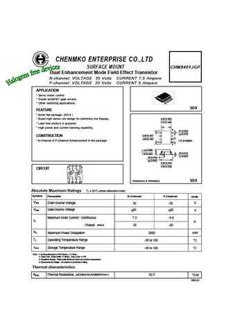
CHENMKO ENTERPRISE CO.,LTD SURFACE MOUNT CHM8401JGP Dual Enhancement Mode Field Effect Transistor N-channel VOLTAGE 30 Volts CURRENT 7.5 Ampere P-channel VOLTAGE 30 Volts CURRENT 5 Ampere APPLICATION * Servo motor control. * Power MOSFET gate drivers. * Other switching applications. SO-8 FEATURE * Small flat package. (SO-8 ) ( ) * Super high dense cell design for extremely low R
fhp840b.pdf
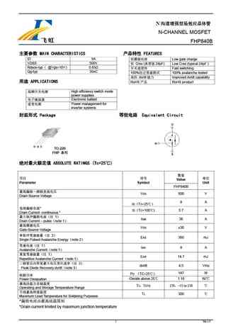
N N-CHANNEL MOSFET FHP840B MAIN CHARACTERISTICS FEATURES ID 9A Low gate charge VDSS 500V Crss ( 24pF) Low Crss (typical 24pF ) Rdson-typ @Vgs=10V 0.65 Fast switching Qg-typ 35nC 100% 100% avalanche tested dv/dt Improved dv/dt c
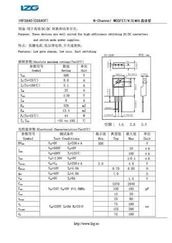
cs840.pdf
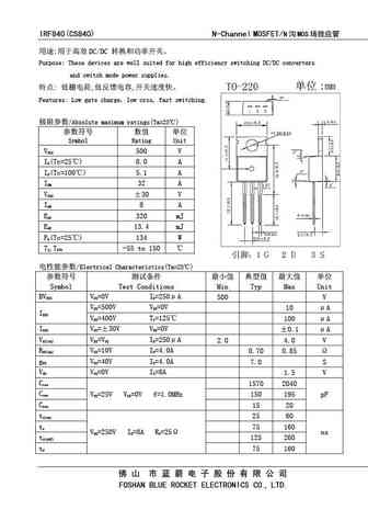
IRF840(CS840) N-Channel MOSFET/N MOS DC/DC Purpose These devices are well suited for high efficiency switching DC/DC converters and switch mode power supplies. , , Features Low gate charge, low crss, fast switching. /Absolute maximum ratings(Ta=25 )
kia840s.pdf
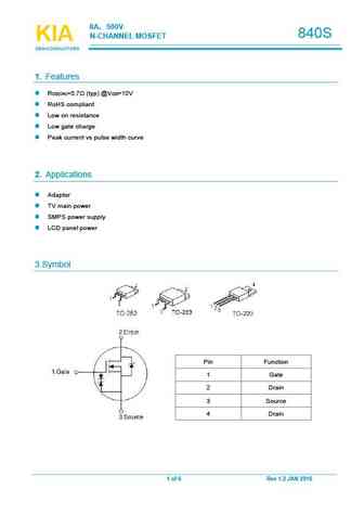
8A 500V 840S N-CHANNELMOSFET KIA KIA KIA SEMICONDUCTORS SEMICONDUCTORS SEMICONDUCTORS 1. Features R =0.7 (typ) @V =10V DS(ON) GS RoHS compliant Low on resistance Low gate charge Peak current vs pulse width curve 2. Applications Adaptor TVmain power SMPSpower supply LCDpanel power 3.Symbol Pin Function 1 Gate 2 Drain 3 Source 4 Drain 1 of 6 Rev 1.2 JAN2016
hfs840.pdf
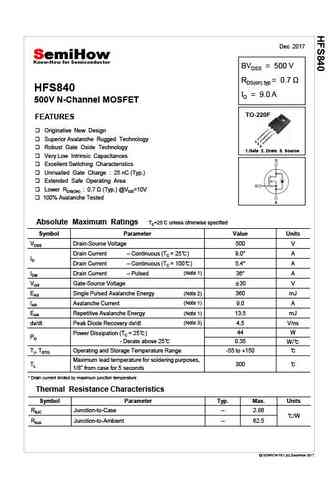
Dec 2017 BVDSS = 500 V RDS(on) typ = 0.7 HFS840 ID = 9.0 A 500V N-Channel MOSFET TO-220F FEATURES Originative New Design Superior Avalanche Rugged Technology 1 2 3 Robust Gate Oxide Technology 1.Gate 2. Drain 3. Source Very Low Intrinsic Capacitances Excellent Switching Characteristics Unrivalled Gate Charge 25 nC (Typ.) Ex
hfp840.pdf
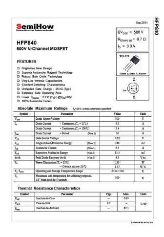
Sep 2011 BVDSS = 500 V RDS(on) typ HFP840 ID = 9.0 A 500V N-Channel MOSFET TO-220 FEATURES Originative New Design 1 2 3 Superior Avalanche Rugged Technology 1.Gate 2. Drain 3. Source Robust Gate Oxide Technology Very Low Intrinsic Capacitances Excellent Switching Characteristics Unrivalled Gate Charge 25 nC (Typ.) Extended Safe Operating Area Lower
hfw840.pdf
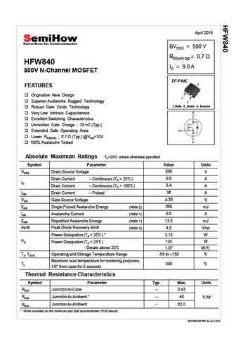
April 2016 BVDSS = 500 V RDS(on) typ HFW840 ID = 9.0 A 500V N-Channel MOSFET D2-PAK 2 FEATURES Originative New Design 1 Superior Avalanche Rugged Technology 3 1.Gate 2. Drain 3. Source Robust Gate Oxide Technology Very Low Intrinsic Capacitances Excellent Switching Characteristics Unrivalled Gate Charge 25 nC (Typ.) Extended Safe Operating Area Lo
sff840 sfp840.pdf
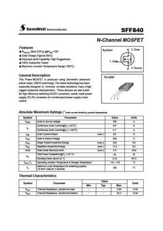
SemiWell Semiconductor SFF840 N-Channel MOSFET Features 2. Drain Symbol RDS(on) (Max 0.85 )@VGS=10V Gate Charge (Typical 38nC) Improved dv/dt Capability, High Ruggedness 1. Gate 100% Avalanche Tested Maximum Junction Temperature Range (150 C) 3. Source General Description TO-220F This Powe
shd218409b.pdf
SENSITRON SHD218409 SHD218409A SEMICONDUCTOR SHD218409B TECHNICAL DATA DATA SHEET 349, REV - HERMETIC POWER MOSFET P-CHANNEL FEATURES -100 Volt, 0.2 Ohm, -18A MOSFET Electrically Isolated Hermetically Sealed Low RDS (on) Equivalent to IRF9140 Series MAXIMUM RATINGS ALL RATINGS ARE AT TA = 25 C UNLESS OTHERWISE SPECIFIED. RATING SYMBOL MIN. TYP. M
tsf840mr.pdf
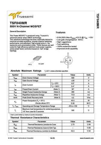
TSF840MR 500V N-Channel MOSFET General Description Features This Power MOSFET is produced using Truesemi s 9.0A,500V,Max.RDS(on)=0.8 @ VGS =10V advanced planar stripe DMOS technology. This advanced technology has been especially tailored to Low gate charge(typical 30nC) minimize on-state resistance, provide superior switching High ruggedness performance, and
tsp840mr tsf840mr.pdf
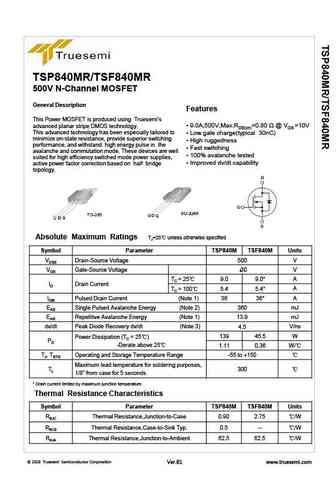
TSP840MR/TSF840MR 500V N-Channel MOSFET General Description Features This Power MOSFET is produced using Truesemi s 9.0A,500V,Max.RDS(on)=0.80 @ VGS =10V advanced planar stripe DMOS technology. This advanced technology has been especially tailored to Low gate charge(typical 30nC) minimize on-state resistance, provide superior switching High ruggedness perfor
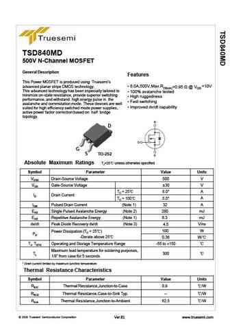
tsf840md.pdf

TSF840MD 500V N-Channel MOSFET General Description Features This Power MOSFET is produced using Truesemi s 8.0A,500V,Max.RDS(on)=0.95 @ VGS =10V advanced planar stripe DMOS technology. This advanced technology has been especially tailored to Low gate charge(typical 30nC) minimize on-state resistance, provide superior switching High ruggedness performance, and
tsd840md.pdf
TSD840MD 500V N-Channel MOSFET General Description Features This Power MOSFET is produced using Truesemi s 8.0A,500V,Max.RDS(on)=0.95 @ VGS =10V advanced planar stripe DMOS technology. This advanced technology has been especially tailored to 100% avalanche tested minimize on-state resistance, provide superior switching High ruggedness performance, and withsta
cs840a8h.pdf
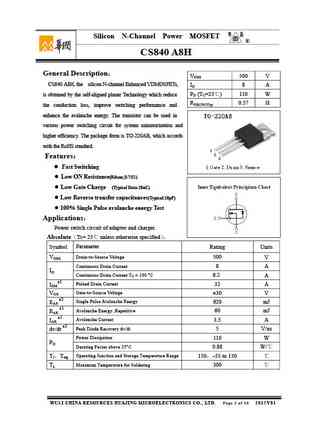
Silicon N-Channel Power MOSFET R CS840 A8H General Description VDSS 500 V CS840 A8H, the silicon N-channel Enhanced VDMOSFETs, ID 8 A PD (TC=25 ) 110 W is obtained by the self-aligned planar Technology which reduce RDS(ON)Typ 0.57 the conduction loss, improve switching performance and enhance the avalanche energy. The transistor can be used in various power s
cs840fa9d.pdf
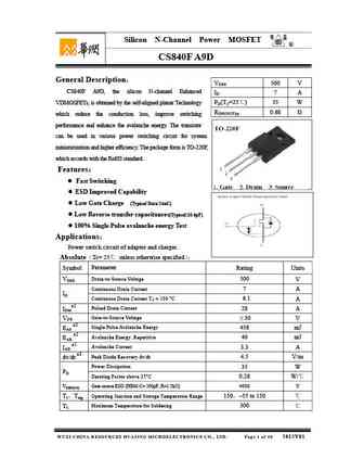
Silicon N-Channel Power MOSFET R CS840F A9D General Description VDSS 500 V CS840F A9D, the silicon N-channel Enhanced ID 7 A PD(TC=25 ) 35 W VDMOSFETs, is obtained by the self-aligned planar Technology RDS(ON)Typ 0.68 which reduce the conduction loss, improve switching performance and enhance the avalanche energy. The transistor can be used in various powe
cs840a8d.pdf

Silicon N-Channel Power MOSFET R CS840 A8D General Description VDSS 500 V CS840 A8D, the silicon N-channel Enhanced ID 7 A PD(TC=25 ) 100 W VDMOSFETs, is obtained by the self-aligned planar RDS(ON)Typ 0.68 Technology which reduce the conduction loss, improve switching performance and enhance the avalanche energy. The transistor can be used in various power
cs840fa9h.pdf

Silicon N-Channel Power MOSFET R CS840F A9H General Description VDSS 500 V CS840F A9H, the silicon N-channel Enhanced ID 8 A PD (TC=25 ) 45 W VDMOSFETs, is obtained by the self-aligned planar Technology RDS(ON)Typ 0.57 which reduce the conduction loss, improve switching performance and enhance the avalanche energy. The transistor can be used in various pow
hd840u hu840u.pdf
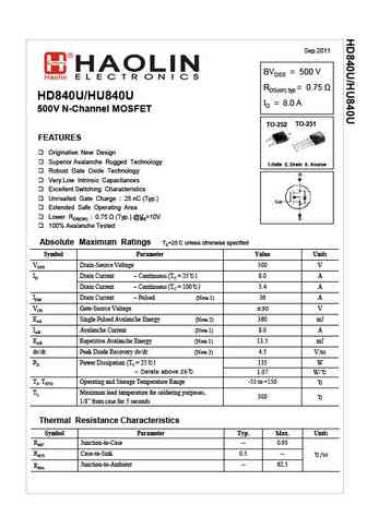
Sep 2011 BVDSS = 500 V RDS(on) typ = 0.75 HD840U/HU840U ID = 8.0 A 500V N-Channel MOSFET TO-251 TO-252 FEATURES Originative New Design Superior Avalanche Rugged Technology 1.Gate 2. Drain 3. Source Robust Gate Oxide Technology Very Low Intrinsic Capacitances Excellent Switching Characteristics Unrivalled Gate Charge 25 nC (Typ.) Ex
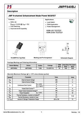
jmpf840bj.pdf
JMPF840BJ Description JMP N-channel Enhancement Mode Power MOSFET Features Applications 500V, 9A Load Switch RDS(ON)
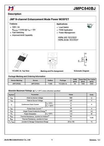
jmpc840bj.pdf
JMPC840BJ Description JMP N-channel Enhancement Mode Power MOSFET Features Applications 500V, 9A Load Switch RDS(ON)
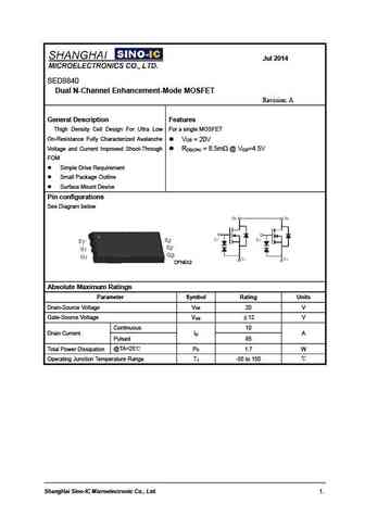
sed8840.pdf
Jul 2014 SED8840 Dual N-Channel Enhancement-Mode MOSFET Revision A General Description Features Thigh Density Cell Design For Ultra Low For a single MOSFET On-Resistance Fully Characterized Avalanche V =20V DS Voltage and Current Improved Shoot-Through R =8.5m @V =4.5V DS(ON) GS FOM Simple Drive Requirement Small Package Outline Surface Mount Device Pin c
sm4840prl.pdf
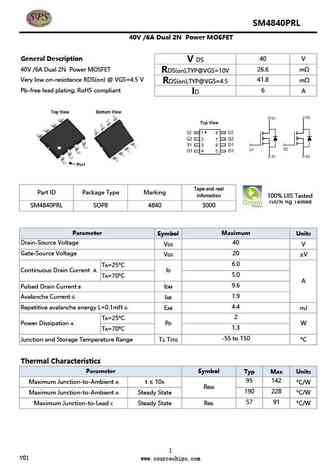
SM4840PRL 40V /6A Dual 2N Power MOSFET C B04C B 40V /6A Dual 2N Power MOSFET 6B04C General Description 40 V V DS 40V /6A Dual 2N Power MOSFET 26.6 m RDS(on),TYP@VGS=10V Very low on-resistance RDS(on) @ VGS=4.5 V 41.8 m RDS(on),TYP@VGS=4.5 Pb-free lead plating; RoHS compliant 6 A ID Tape and reel Part ID Package Type Marking infomation 100% UIS Tested 100% Rg Tested SM4840PR
irfi840gpbf.pdf
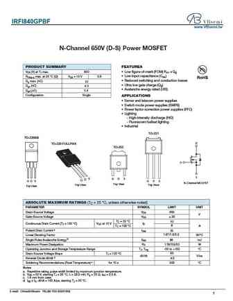
IRFI840GPBF www.VBsemi.tw N hannel 650 D S Power MOSFET FEATURES PRODUCT SUMMARY VDS (V) at TJ max. 650 Low figure-of-merit (FOM) Ron x Qg Low input capacitance (Ciss) RDS(on) max. at 25 C ( ) VGS = 10 V 0.9 Reduced switching and conduction losses Qg max. (nC) 57 Ultra low gate charge (Qg) Qgs (nC) 4.0 Avalanche energy rated (UIS) Qgd (nC) 5.4 Configur
buk9840-55.pdf
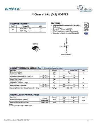
BUK9840-55 www.VBsemi.tw N-Channel 60-V (D-S) MOSFET FEATURES PRODUCT SUMMARY Halogen-free According to IEC 61249-2-21 VDS (V) RDS(on) ( )ID (A) Definition 0.029 at VGS = 10 V 7.0 TrenchFET Power MOSFETs 60 0.033 at VGS = 4.5 V 5.6 175 C Maximum Junction Temperature Compliant to RoHS Directive 2002/95/EC D SOT-223 D G S D G S N-Channel MOSFET
ao4840.pdf
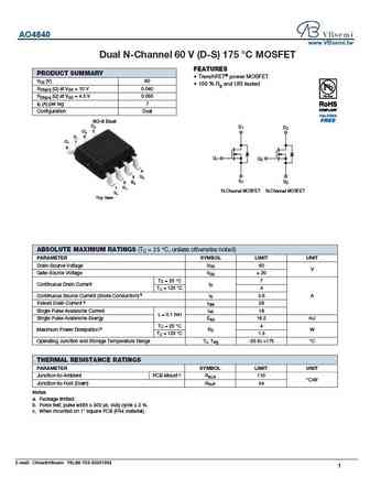
AO4840 www.VBsemi.tw Dual N-Channel 60 V (D-S) 175 C MOSFET FEATURES PRODUCT SUMMARY TrenchFET power MOSFET VDS (V) 60 100 % Rg and UIS tested RDS(on) ( ) at VGS = 10 V 0.040 RDS(on) ( ) at VGS = 4.5 V 0.055 ID (A) per leg 7 Configuration Dual SO-8 Dual D2 D1 D2 D2 5 D1 6 D1 7 8 G1 G2 4 G2 3 3 S1 S2 S2 S2 2 2 G G1 1 1 N-Channel MOSFET N-Channel M
si4840dy-t1-e3.pdf
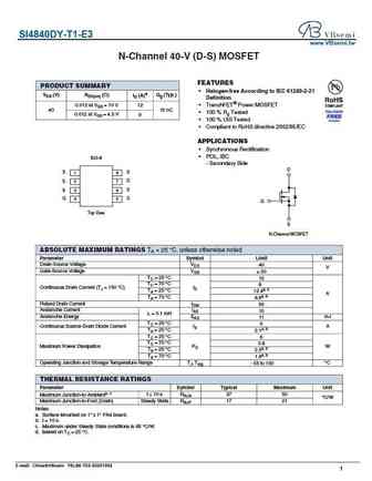
SI4840DY-T1-E3 www.VBsemi.tw N-Channel 40-V (D-S) MOSFET FEATURES PRODUCT SUMMARY Halogen-free According to IEC 61249-2-21 VDS (V) RDS(on) ( ) ID (A)d Qg (Typ.) Definition 0.012 at VGS = 10 V TrenchFET Power MOSFET 12 40 15 nC 100 % Rg Tested 0.012 at VGS = 4.5 V 9 100 % UIS Tested Compliant to RoHS directive 2002/95/EC APPLICATIONS Synchron
tpp60r840c tpa60r840c tpu60r840c tpd60r840c tpc60r840c tpb60r840c.pdf
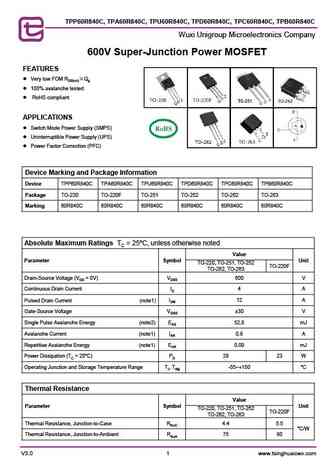
TPP60R840C, TPA60R840C, TPU60R840C, TPD60R840C, TPC60R840C, TPB60R840C Wuxi Unigroup Microelectronics Company 600V Super-Junction Power MOSFET FEATURES Very low FOM RDS(on) Qg 100% avalanche tested RoHS compliant APPLICATIONS Switch Mode Power Supply (SMPS) Uninterruptible Power Supply (UPS) Power Factor Correction (PFC) Device Marking and Package
hm4840.pdf
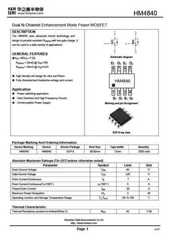
HM4840 Dual N-Channel Enhancement Mode Power MOSFET DESCRIPTION The HM4840 uses advanced trench technology and design to provide excellent RDS(ON) with low gate charge. It can be used in a wide variety of applications. GENERAL FEATURES Schematic diagram VDS =40V,ID =7.0A RDS(ON)
bss8402dw.pdf
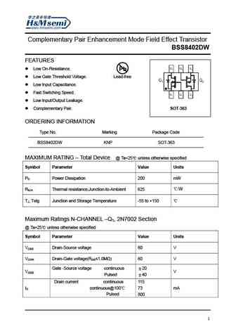
Complementary Pair Enhancement Mode Field Effect Transistor BSS8402DW FEATURES Low On-Resistance. Pb Low Gate Threshold Voltage. Lead-free Low Input Capacitance. Fast Switching Speed. Low Input/Output Leakage. Complementary Pair. SOT-363 ORDERING INFORMATION Type No. Marking Package Code BSS8402DW KNP SOT-363 MAXIMUM RATING Total Device @ Ta
hm840 hm840f.pdf
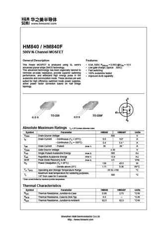
840 / 840F 500V N-Channel MOSFET General Description Features This Power MOSFET is produced using SL semi s 9.0A, 500V, RDS(on) = 0.85 @VGS = 10 V advanced planar stripe DMOS technology. Low gate charge ( typical 30nC) This advanced technology has been especially tailored to Fast switching minimize on-state resistance, provide superior switching 100% avalanche
irf840.pdf
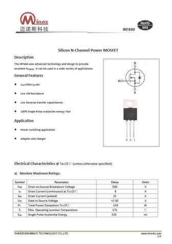
IRF840 SiliconN-Channel Power MOSFET Description The IRF840 uses advanced technology and design to provide excellent R . It can be used in a wide variety of applications. DS(ON) General Features V =500V,I =8A DS D Low ON Resistance Low Reverse transfer capacitances 100% Single Pulse avalanche energy Test Application Power switching application Adapter and charger Electrical
ytf840.pdf
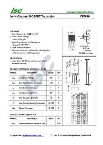
isc N-Channel MOSFET Transistor YTF840 FEATURES Drain Current I = 8A@ T =25 D C Drain Source Voltage V = 500V(Min) DSS Static Drain-Source On-Resistance R =0.85 (Max) DS(on) 100% avalanche tested Minimum Lot-to-Lot variations for robust device performance and reliable operation DESCRIPTION motor drive, DC-DC converter, power switch and solenoid drive. ABSOL
irf840.pdf
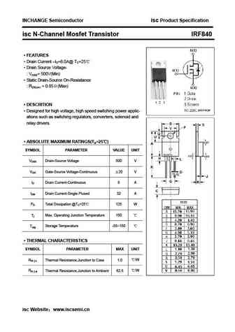
INCHANGE Semiconductor isc Product Specification isc N-Channel Mosfet Transistor IRF840 FEATURES Drain Current ID=8.0A@ TC=25 Drain Source Voltage- VDSS= 500V(Min) Static Drain-Source On-Resistance RDS(on) = 0.85 (Max) DESCRITION Designed for high voltage, high speed switching power applic- ations such as switching regulators, converters, solenoid an
bd840.pdf
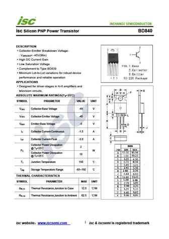
INCHANGE Semiconductor isc Silicon PNP Power Transistor BD840 DESCRIPTION Collector-Emitter Breakdown Voltage- V = -45V(Min) (BR)CEO High DC Current Gain Low Saturation Voltage Complement to Type BD839 Minimum Lot-to-Lot variations for robust device performance and reliable operation APPLICATIONS Designed for driver-stages in hi-fi amplifiers and television circuits.
2n5838 2n5839 2n5840.pdf
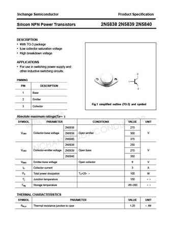
Inchange Semiconductor Product Specification Silicon NPN Power Transistors 2N5838 2N5839 2N5840 DESCRIPTION With TO-3 package Low collector saturation voltage High breakdown voltage APPLICATIONS For use in switching power supply and other inductive switching circuits. PINNING PIN DESCRIPTION 1 Base 2 Emitter Fig.1 simplified outline (TO-3) and symbol 3 Collecto
irf840lc.pdf
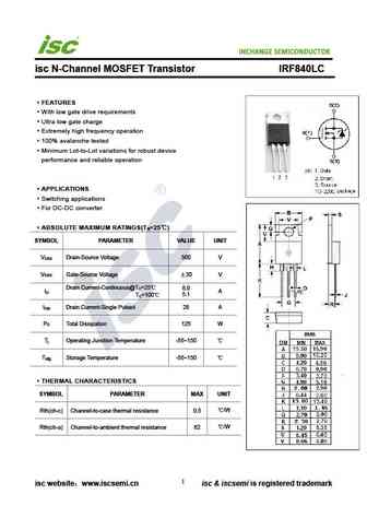
INCHANGE Semiconductor isc N-Channel MOSFET Transistor IRF840LC FEATURES With low gate drive requirements Ultra low gate charge Extremely high frequency operation 100% avalanche tested Minimum Lot-to-Lot variations for robust device performance and reliable operation APPLICATIONS Switching applications For DC-DC converter ABSOLUTE MAXIMUM RATINGS(T =25 ) a SY
irf840a.pdf
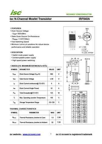
isc N-Channel Mosfet Transistor IRF840A FEATURES Drain Source Voltage- V = 500V(Min) DSS Static Drain-Source On-Resistance R = 0.85 (Max) DS(on) Fast Switching Speed Minimum Lot-to-Lot variations for robust device performance and reliable operation DESCRITION Switch mode power supply Uninterruptable power supply High speed power switching ABSOLUTE MAXIMUM
2sd1840.pdf
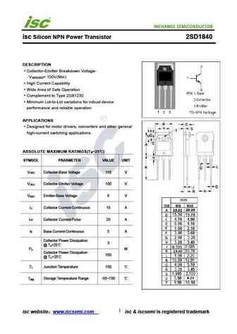
isc Silicon NPN Power Transistor 2SD1840 DESCRIPTION Collector-Emitter Breakdown Voltage- V = 100V(Min) (BR)CEO High Current Capability Wide Area of Safe Operation Complement to Type 2SB1230 Minimum Lot-to-Lot variations for robust device performance and reliable operation APPLICATIONS Designed for motor drivers, converters and other general high-current switching appl
Другие MOSFET... 5N20A , 630A , 640 , 18N20 , 18N20A , 2N25 , 3N25 , 740 , 50N06 , 16N50F , 13N50F , 20N50 , 5N60F , 7N60F , 8N60A , 8N60AF , 10N60F .
🌐 : EN ES РУ

Список транзисторов
Обновления
MOSFET: ASD80R750E | ASD70R950E | ASD70R600E | ASD70R380E | ASD65R850E | ASD65R550E | ASD65R350E | ASD65R300E | ASD65R280E | ASD65R270E | ASD60R330E | ASD60R280E | ASB80R750E | ASB70R380E | ASB65R300E | ASB65R220E
Popular searches
2n4401 datasheet | irf640 | irf840 | irf740 | c945 transistor | irf640n | 2n3904 | bc547 datasheet