AO3405. Аналоги и основные параметры
Наименование производителя: AO3405
Тип транзистора: MOSFET
Полярность: P
Предельные значения
Pd ⓘ - Максимальная рассеиваемая мощность: 1.4 W
|Vds|ⓘ - Максимально допустимое напряжение сток-исток: 30 V
|Vgs|ⓘ - Максимально допустимое напряжение затвор-исток: 12 V
|Id| ⓘ - Максимально допустимый постоянный ток стока: 2.6 A
Tj ⓘ - Максимальная температура канала: 150 °C
Электрические характеристики
tr ⓘ - Время нарастания: 8.8 ns
Cossⓘ - Выходная емкость: 54 pf
RDSonⓘ - Сопротивление сток-исток открытого транзистора: 0.13 Ohm
Тип корпуса: SOT23
Аналог (замена) для AO3405
- подборⓘ MOSFET транзистора по параметрам
AO3405 даташит
ao3405.pdf
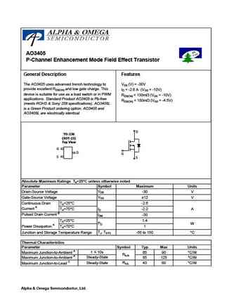
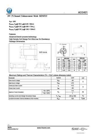
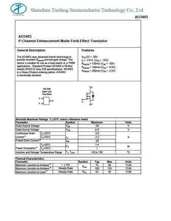
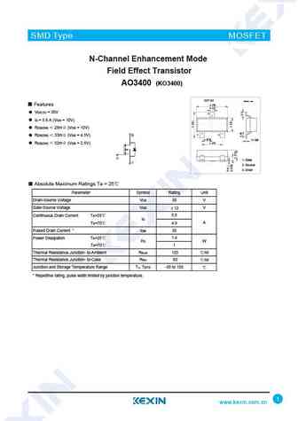
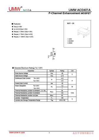
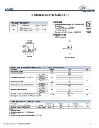
AO3405 P-Channel Enhancement Mode Field Effect Transistor General Description Features The AO3405 uses advanced trench technology to VDS (V) = -30V provide excellent RDS(ON) and low gate charge. This ID = -2.6 A (VGS = -10V) device is suitable for use as a load switch or in PWM RDS(ON)
ao3409 ao3409l.pdf
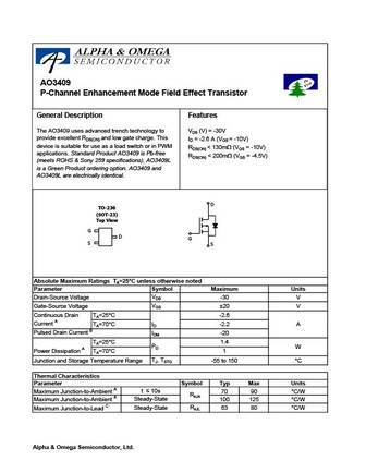
AO3409 P-Channel Enhancement Mode Field Effect Transistor General Description Features The AO3409 uses advanced trench technology to VDS (V) = -30V provide excellent RDS(ON) and low gate charge. This ID = -2.6 A (VGS = -10V) device is suitable for use as a load switch or in PWM RDS(ON)
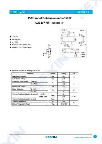
ao3407 a7 a79t x7kv code psot23.pdf
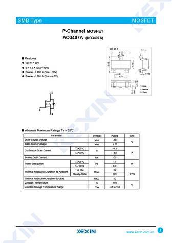
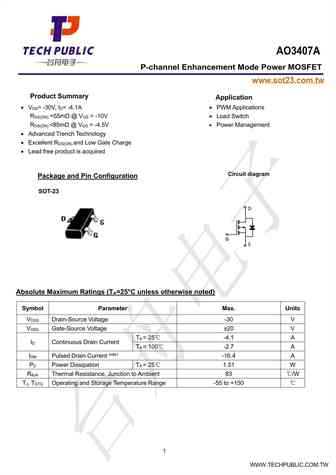
SMD Type MOSFET P-Channel MOSFET AO3407A (KO3407A) SOT-23-3 Unit mm +0.2 2.9 -0.1 +0.1 0.4 -0.1 3 Features VDS (V) =-30V ID =-4.3 A (VGS =-10V) 1 2 RDS(ON) 48m (VGS =-10V) +0.02 +0.1 0.15 -0.02 0.95-0.1 +0.1 1.9-0.2 RDS(ON) 78m (VGS =-4.5V) 1. Gate 2. Source 3. Drain D D G G S S Absolute Maximum Ratings Ta = 25 Paramete
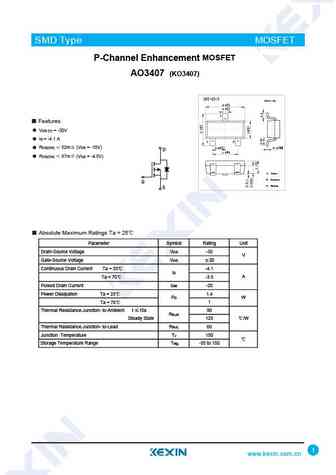
ao3407.pdf
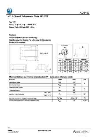
AO3407 30V P-Channel Enhancement Mode MOSFET V = -30V DS R , V DS(ON) gs@-10V, I 4.1A
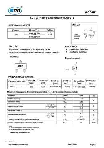
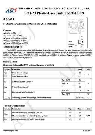
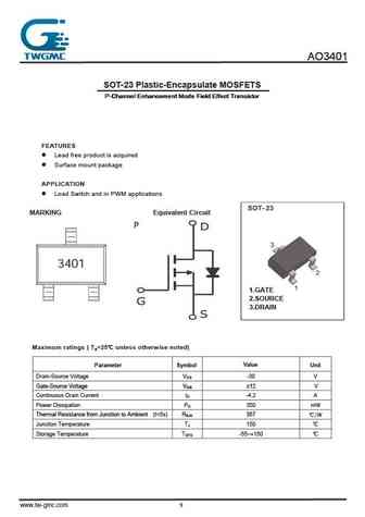
ao3401.pdf
AO3401 30V P-Channel Enhancement Mode MOSFET V = -30V DS R , V DS(ON) gs@-10V, I ds@-4.2A
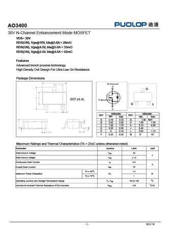
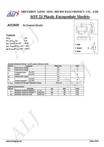
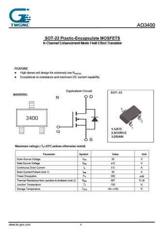
ao3400.pdf
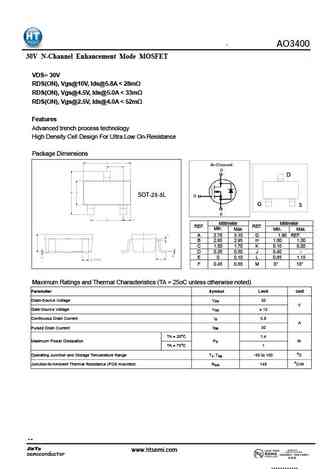
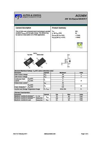
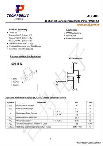
AO3400 30V N-Channel Enhancement Mode MOSFET VDS= 30V RDS(ON), Vgs@10V, Ids@5.8A
ao3401.pdf
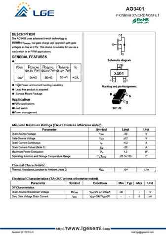
AO3401 P-Channel 30V(D-S) MOSFET DESCRIPTION D The AO3401 uses advanced trench technology to provide excellent RDS(ON), low gate charge and operation with gate G voltages as low as 2.5V. This device is suitable for use as a load switch or in PWM applications. S GENERAL FEATURES Schematic diagram VDSS RDS(ON) RDS(ON) RDS(ON) ID @ 4.5V (Typ) @ 2.5V (Typ) @ 10V (Typ)
ao3400.pdf
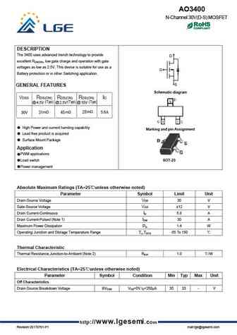
AO3400 N-Channel 30V(D-S) MOSFET DESCRIPTION The 3400 uses advanced trench technology to provide D excellent RDS(ON), low gate charge and operation with gate voltages as low as 2.5V. This device is suitable for use as a G Battery protection or in other Switching application. S GENERAL FEATURES Schematic diagram VDSS RDS(ON) RDS(ON) RDS(ON) ID @ 4.5V (Typ) @ 2.5V (Typ) @ 1
ao3409.pdf

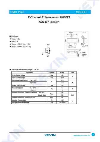
AO3409 30V P-Channel MOSFET General Description Product Summary VDS -30V The AO3409 uses advanced trench technology to provide excellent RDS(ON) and low gate charge. This device is ID (at VGS=-10V) -2.6A suitable for use as a load switch or in PWM applications. RDS(ON) (at VGS=-10V)
ao3407.pdf
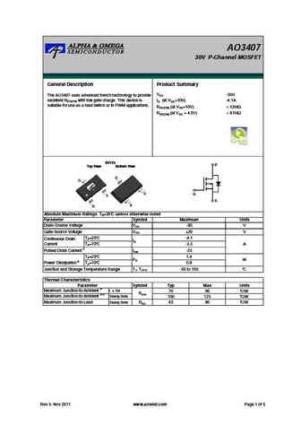
AO3407 30V P-Channel MOSFET General Description Product Summary VDS -30V The AO3407 uses advanced trench technology to provide excellent RDS(ON) with low gate charge. This device is ID (at VGS=10V) -4.1A suitable for use as a load switch or in PWM applications. RDS(ON) (at VGS=10V)
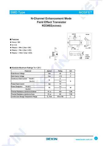
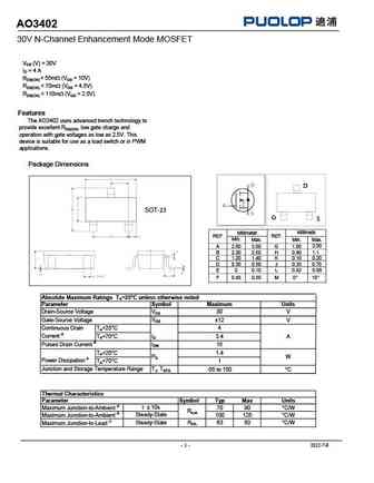
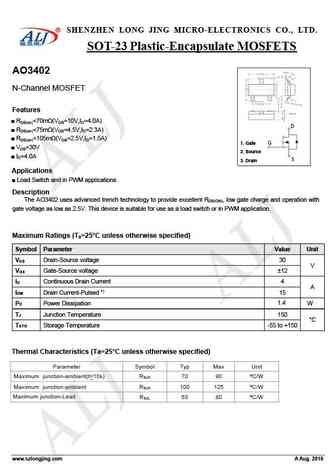
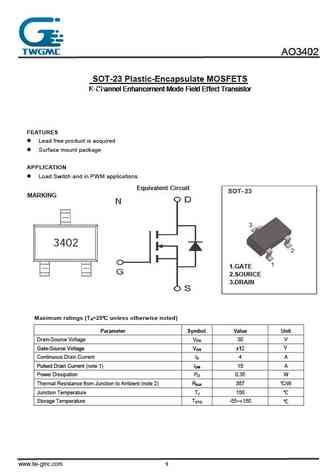
ao3402.pdf

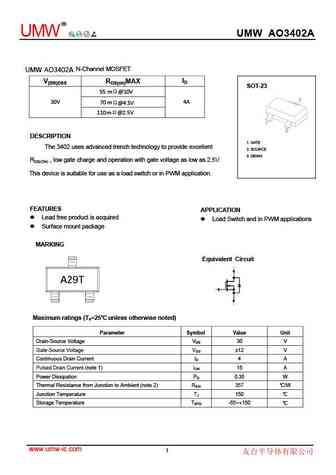
AO3402 30V N-Channel MOSFET General Description Product Summary VDS 30V The AO3402 uses advanced trench technology to provide excellent RDS(ON), low gate charge and operation with gate ID (at VGS=10V) 4A voltages as low as 2.5V. This device is suitable for use as RDS(ON) (at VGS=10V)
ao3406.pdf

AO3406 30V N-Channel MOSFET General Description Product Summary VDS 30V The AO3406 uses advanced trench technology to provide excellent RDS(ON) and low gate charge. This device is ID (at VGS=10V) 3.6A suitable for use as a load switch or in PWM applications. RDS(ON) (at VGS=10V)
ao3403.pdf
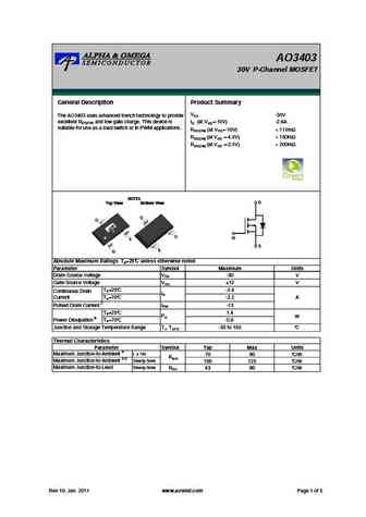
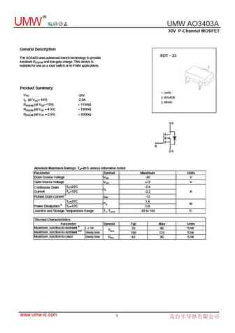
AO3403 30V P-Channel MOSFET General Description Product Summary VDS The AO3403 uses advanced trench technology to provide -30V excellent RDS(ON) and low gate charge. This device is ID (at VGS=-10V) -2.6A suitable for use as a load switch or in PWM applications. RDS(ON) (at VGS=-10V)

ao3401.pdf
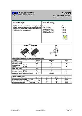
AO3401 30V P-Channel MOSFET General Description Product Summary VDS -30V The AO3401 uses advanced trench technology to provide excellent RDS(ON), low gate charge and operation with gate ID (at VGS=-10V) -4.0A voltages as low as 2.5V. This device is suitable for use as RDS(ON) (at VGS=-10V)
ao3400c.pdf
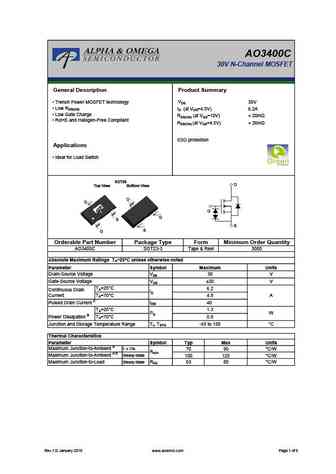
AO3400C 30V N-Channel MOSFET General Description Product Summary VDS Trench Power MOSFET technology 30V Low RDS(ON) ID (at VGS=4.5V) 6.2A Low Gate Charge RDS(ON) (at VGS=10V)
ao3401a.pdf
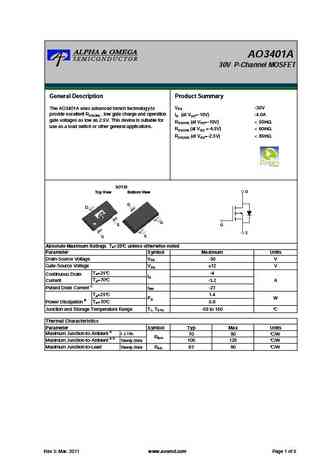
AO3401A 30V P-Channel MOSFET General Description Product Summary VDS -30V The AO3401A uses advanced trench technology to provide excellent RDS(ON) , low gate charge and operation ID (at VGS=-10V) -4.0A gate voltages as low as 2.5V. This device is suitable for RDS(ON) (at VGS=-10V)
ao3407a.pdf
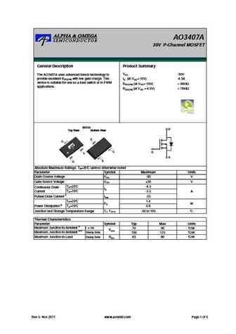
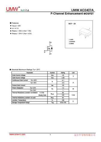
AO3407A 30V P-Channel MOSFET General Description Product Summary VDS -30V The AO3407A uses advanced trench technology to provide excellent RDS(ON) with low gate charge. This ID (at VGS=-10V) -4.3A device is suitable for use as a load switch or in PWM RDS(ON) (at VGS=-10V)
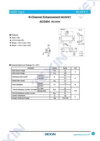
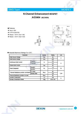
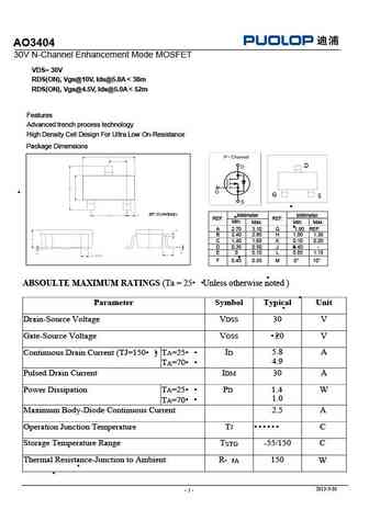
ao3404.pdf
AO3404 30V N-Channel MOSFET General Description Product Summary VDS 30V The AO3404 uses advanced trench technology to provide excellent RDS(ON) and low gate charge. This device may ID (at VGS=10V) 5A be used as a load switch or in PWM applications. RDS(ON) (at VGS=10V)
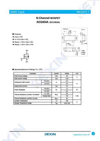
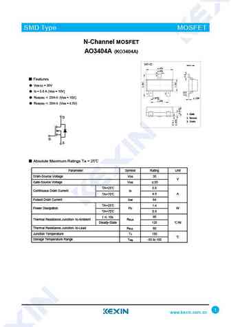
ao3404a.pdf
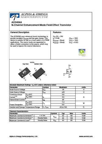
AO3404A N-Channel Enhancement Mode Field Effect Transistor General Description Features The AO3404A uses advanced trench technology to VDS (V) = 30V provide excellent RDS(ON) and low gate charge. This ID = 5.8A (VGS = 10V) device is suitable for use as a load switch or in PWM RDS(ON)
ao3400.pdf
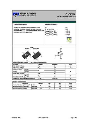
AO3400 30V N-Channel MOSFET General Description Product Summary VDS 30V The AO3400 combines advanced trench MOSFET technology with a low resistance package to provide ID (at VGS=10V) 5.8A extremely low RDS(ON). This device is suitable for use as a RDS(ON) (at VGS=10V)
ao3409.pdf
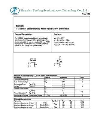
Shenzhen Tuofeng Semiconductor Technology Co., Ltd AO3409 AO3409 P-Channel Enhancement Mode Field Effect Transistor General Description Features The AO3409 uses advanced trench technology to VDS (V) = -30V provide excellent RDS(ON) and low gate charge. This ID = -2.6 A (VGS = -10V) device is suitable for use as a load switch or in PWM RDS(ON)
ao3407.pdf
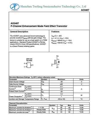
Shenzhen Tuofeng Semiconductor Technology Co., Ltd AO3407 AO3407 P-Channel Enhancement Mode Field Effect Transistor General Description Features The AO3407 uses advanced trench technology to VDS (V) = -30V provide excellent RDS(ON) with low gate charge. This ID = -4.1 A (VGS = -10V) device is suitable for use as a load switch or in PWM RDS(ON)
ao3402.pdf

Shenzhen Tuofeng Semiconductor Technology Co., Ltd AO3402 AO3402 N-Channel Enhancement Mode Field Effect Transistor General Description Features The AO3402 uses advanced trench technology to VDS (V) = 30V provide excellent RDS(ON), low gate charge and ID = 4 A operation with gate voltages as low as 2.5V. This RDS(ON)
ao3406.pdf
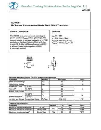
Shenzhen Tuofeng Semiconductor Technology Co., Ltd AO3406 AO3406 N-Channel Enhancement Mode Field Effect Transistor General Description Features The AO3406 uses advanced trench technology to VDS (V) = 30V provide excellent RDS(ON) and low gate charge. This ID = 3.6A (VGS = 10V) device is suitable for use as a load switch or in PWM RDS(ON)
ao3403.pdf
Shenzhen Tuofeng Semiconductor Technology Co., Ltd AO3403 AO3403 P-Channel Enhancement Mode Field Effect Transistor General Description Features The AO3403 uses advanced trench technology to VDS (V) = -30V provide excellent RDS(ON) and low gate charge. This ID = -2.6 A (VGS = -10V) device is suitable for use as a load switch or in PWM RDS(ON)
ao3401.pdf
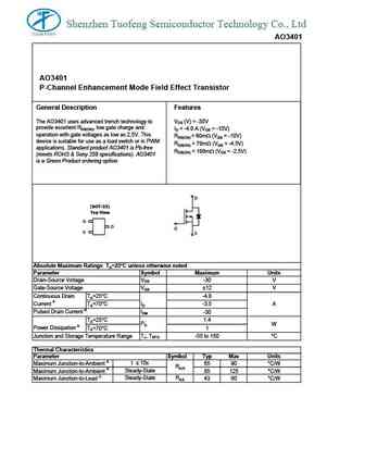
Shenzhen Tuofeng Semiconductor Technology Co., Ltd AO3401 AO3401 P-Channel Enhancement Mode Field Effect Transistor General Description Features The AO3401 uses advanced trench technology to VDS (V) = -30V provide excellent RDS(ON), low gate charge and ID = -4.0 A (VGS = -10V) operation with gate voltages as low as 2.5V. This RDS(ON)
ao3404.pdf
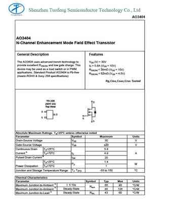
Shenzhen Tuofeng Semiconductor Technology Co., Ltd AO3404 AO3404 N-Channel Enhancement Mode Field Effect Transistor General Description Features The AO3404 uses advanced trench technology to VDS (V) = 30V provide excellent RDS(ON) and low gate charge. This ID = 5.8A (VGS = 10V) device may be used as a load switch or in PWM RDS(ON)
ao3400.pdf
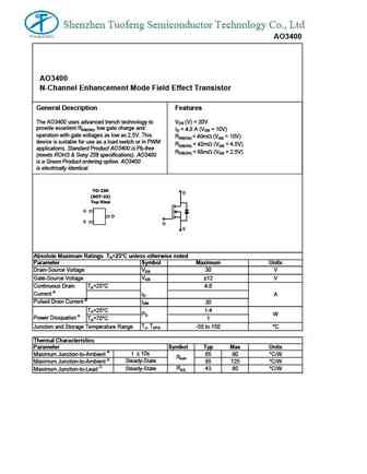
Shenzhen Tuofeng Semiconductor Technology Co., Ltd AO3400 AO3400 N-Channel Enhancement Mode Field Effect Transistor General Description Features The AO3400 uses advanced trench technology to VDS (V) = 30V provide excellent RDS(ON), low gate charge and ID = 4.8 A (VGS = 10V) operation with gate voltages as low as 2.5V. This RDS(ON)
ao3401.pdf
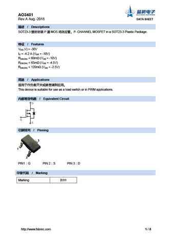
AO3401 Rev.A Aug.-2016 DATA SHEET / Descriptions SOT23-3 P MOS P- CHANNEL MOSFET in a SOT23-3 Plastic Package. / Features VDS (V) = -30V ID = -4.2 A (VGS = -10V) RDS(ON)
ao3400.pdf
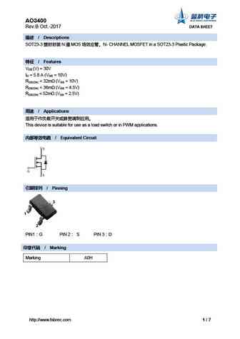
AO3400 Rev.B Oct.-2017 DATA SHEET / Descriptions SOT23-3 N MOS N- CHANNEL MOSFET in a SOT23-3 Plastic Package. / Features VDS (V) = 30V ID = 5.8 A (VGS = 10V) RDS(ON)
ao3404-3.pdf
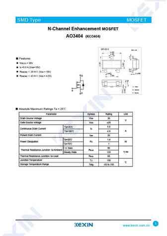
SMD Type IC SMD Type MOSFET N-Channel Enhancement MOSFET AO3404 (KO3404) SOT-23-3 Unit mm +0.2 2.9 -0.1 +0.1 0.4-0.1 3 Features VDS (V) = 30V ID =5.8 A (VGS=10V) 1 2 RDS(ON) 28 m (VGS = 10V) +0.02 +0.1 0.15 -0.02 0.95 -0.1 +0.1 1.9 -0.2 D RDS(ON) 43 m (VGS = 4.5V) 1. Gate 2. Source G 3. Drain S Absolute Maximum Ratings Ta = 25 Parameter Symbol Rating Unit Drain
ao3409.pdf
SMD Type MOSFET P-Channel Enhancement Mode Field Effect Transistor AO3409 (KO3409) SOT-23 Unit mm +0.1 2.9 -0.1 +0.1 0.4 -0.1 Features 3 VDS (V) = -30V ID = -2.6 A (VGS = -10V) 1 2 RDS(ON)
ao3401hf.pdf
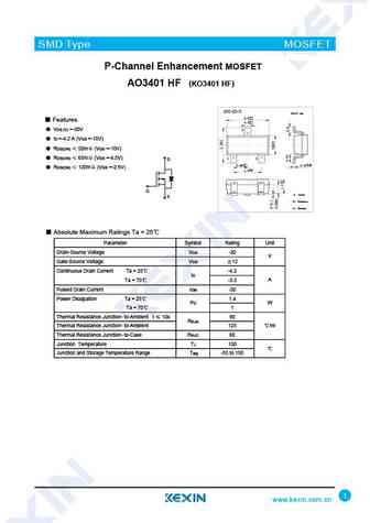
SMD Type MOSFET P-Channel Enhancement MOSFET AO3401 HF (KO3401 HF) SOT-23-3 Unit mm +0.2 2.9 -0.1 Features +0.1 0.4-0.1 VDS (V) =-30V 3 ID =-4.2 A (VGS =-10V) RDS(ON) 50m (VGS =-10V) RDS(ON) 65m (VGS =-4.5V) 1 2 D +0.02 +0.1 0.15 -0.02 0.95 -0.1 RDS(ON) 120m (VGS =-2.5V) +0.1 1.9 -0.2 G 1. Gate S 2. Source 3. Drain A
ao3407.pdf
SMD Type IC SMD Type MOSFET P-Channel Enhancement MOSFET AO3407 (KO3407) SOT-23 Unit mm +0.1 2.9 -0.1 +0.1 0.4 -0.1 Features 3 VDS (V) = -30V ID = -4.1 A 1 2 RDS(ON) 52m (VGS = -10V) D +0.1 +0.05 0.95 -0.1 0.1 -0.01 +0.1 RDS(ON) 87m (VGS = -4.5V) 1.9 -0.1 1.Base 1. Gate 2.Emitter 2. Source G 3. Drain 3.collector S Absolute Maximum Ratings Ta = 25 Parameter Sy
ao3407 ko3407.pdf

SMD Type IC SMD Type MOSFET P-Channel Enhancement MOSFET AO3407 (KO3407) SOT-23-3 Unit mm +0.2 2.9-0.1 +0.1 0.4 -0.1 3 Features VDS (V) = -30V ID = -4.1 A 1 2 +0.02 +0.1 0.15 -0.02 RDS(ON) 52m (VGS = -10V) 0.95 -0.1 D 1.9+0.1 -0.2 RDS(ON) 87m (VGS = -4.5V) 1. Gate 2. Source G 3. Drain S Absolute Maximum Ratings Ta = 25 Parameter Symbol Rating Unit Drain-Sourc
ao3402.pdf
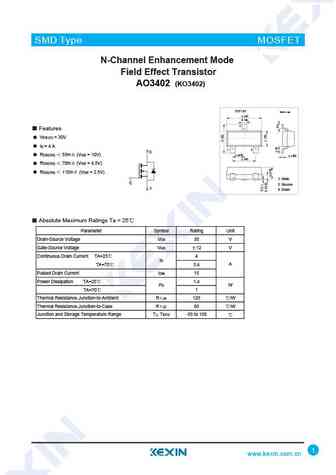
SMD Type IC SMD Type MOSFET N-Channel Enhancement Mode Field Effect Transistor AO3402 (KO3402) SOT-23 Unit mm +0.1 2.9 -0.1 +0.1 0.4 -0.1 3 Features VDS (V) = 30V ID = 4 A 1 2 +0.1 +0.05 RDS(ON) 55m (VGS = 10V) 0.95 -0.1 0.1 -0.01 +0.1 1.9 -0.1 RDS(ON) 70m (VGS = 4.5V) RDS(ON) 110m (VGS = 2.5V) 1.Base 1. Gate 2.Emitter 2. Source 3. Drain 3.collector Absolute Maximu
ao3402 ko3402.pdf

SMD Type IC SMD Type MOSFET N-Channel Enhancement MOSFET AO3402 (KO3402) SOT-23-3 Unit mm +0.2 2.9 -0.1 Features +0.1 0.4 -0.1 VDS (V) = 30V 3 ID = 4 A RDS(ON) 55m (VGS = 10V) RDS(ON) 70m (VGS = 4.5V) 1 2 +0.02 +0.1 0.15 -0.02 D 0.95 -0.1 RDS(ON) 110m (VGS = 2.5V) +0.1 1.9 -0.2 1. Gate G 2. Source S 3. Drain Absolute Maximum Ratings Ta = 25 Parameter Symbol Rating
ao3403-3.pdf
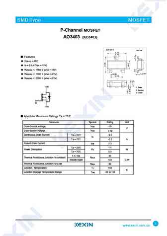
SMD Type MOSFET P-Channel MOSFET AO3403 (KO3403) SOT-23-3 Unit mm +0.2 2.9-0.1 +0.1 0.4 -0.1 Features 3 VDS (V) =-30V ID =-2.6 A (VGS =-10V) RDS(ON) 115m (VGS =-10V) 1 2 +0.02 +0.1 0.15 -0.02 0.95 -0.1 RDS(ON) 150m (VGS =-4.5V) +0.1 1.9-0.2 RDS(ON) 200m (VGS =-2.5V) D D 1. Gate 2. Source 3. Drain G G S S Absolut
ko3400 ao3400.pdf
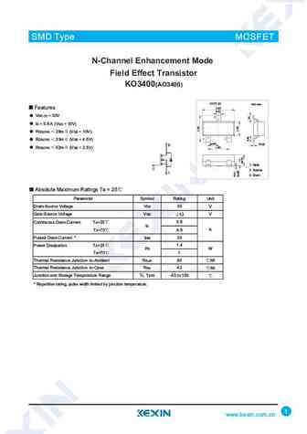
SMD Type IC SMD Type MOSFET N-Channel Enhancement Mode Field Effect Transistor KO3400(AO3400) SOT-23 Unit mm +0.1 Features 2.9-0.1 +0.1 0.4-0.1 VDS (V) = 30V 3 ID =5.8 A(VGS =10V) RDS(ON) 28m (VGS = 10V) 12 RDS(ON) 33m (VGS =4.5V) +0.1 +0.05 0.95-0.1 0.1-0.01 +0.1 1.9-0.1 RDS(ON) 52m (VGS =2.5V) 1.Base 1. Gate 2.Emitter 2. Source 3. Drain 3.collector Absolute Maxim
ao3409 ko3409.pdf
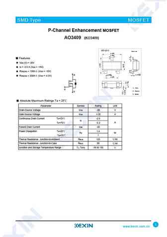
SMD Type MOSFET P-Channel Enhancement MOSFET AO3409 (KO3409) SOT-23-3 Unit mm +0.2 2.9-0.1 +0.1 0.4 -0.1 Features 3 VDS (V) = -30V ID = -2.6 A (VGS = -10V) RDS(ON)
ao3403.pdf
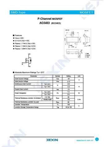
SMD Type MOSFET P-Channel MOSFET AO3403 (KO3403) SOT-23 Unit mm +0.1 2.9-0.1 +0.1 0.4 -0.1 3 Features VDS (V) =-30V ID =-2.6 A (VGS =-10V) 1 2 RDS(ON) 115m (VGS =-10V) +0.05 0.95+0.1 -0.1 0.1 -0.01 RDS(ON) 150m (VGS =-4.5V) 1.9+0.1 -0.1 RDS(ON) 200m (VGS =-2.5V) 1. Gate D D 2. Source 3. Drain G G S S Absolute Max
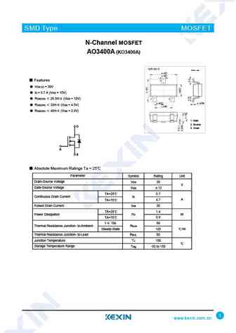
ao3400a.pdf
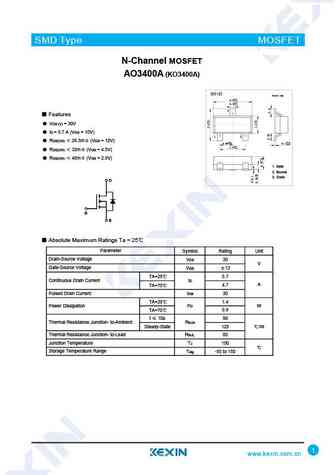
SMD Type MOSFET N-Channel MOSFET AO3400A (KO3400A) SOT-23 Unit mm +0.1 2.9 -0.1 0.4+0.1 -0.1 3 Features VDS (V) = 30V ID = 5.7 A (VGS = 10V) 1 2 RDS(ON) 26.5m (VGS = 10V) +0.1 +0.05 0.95 -0.1 0.1 -0.01 +0.1 1.9 -0.1 RDS(ON) 32m (VGS = 4.5V) RDS(ON) 48m (VGS = 2.5V) 1. Gate 2. Source 3. Drain D D G G S S Absolute
ao3400-3.pdf
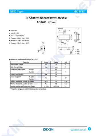
SMD Type IC SMD Type MOSFET N-Channel Enhancement MOSFET AO3400 (KO3400) SOT-23-3 Unit mm +0.2 2.9 -0.1 Features +0.1 0.4-0.1 3 VDS (V) = 30V ID = 5.8 A (VGS = 10V) RDS(ON) 28m (VGS = 10V) 1 2 RDS(ON) 33m (VGS = 4.5V) +0.02 +0.1 0.15 -0.02 0.95 -0.1 RDS(ON) 52m (VGS = 2.5V) D +0.1 1.9 -0.2 1. Gate 2. Source G S 3. Drain Absolute Maximum Ratings Ta = 25 Parameter Sy
ao3401-3.pdf

SMD Type MOSFET P-Channel Enhancement MOSFET AO3401 (KO3401) SOT-23-3 Unit mm +0.2 2.9 -0.1 Features +0.1 0.4-0.1 VDS (V) =-30V 3 ID =-4.2 A (VGS =-10V) RDS(ON) 50m (VGS =-10V) RDS(ON) 65m (VGS =-4.5V) 1 2 D +0.02 +0.1 0.15 -0.02 0.95 -0.1 RDS(ON) 120m (VGS =-2.5V) +0.1 1.9 -0.2 G 1. Gate S 2. Source 3. Drain Absolu
ao3401 ko3401.pdf
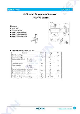
SMD Type MOSFET P-Channel Enhancement MOSFET AO3401 (KO3401) SOT-23 Unit mm 2.9+0.1 -0.1 +0.1 0.4-0.1 Features 3 VDS (V) =-30V ID =-4.2 A (VGS =-10V) RDS(ON) 50m (VGS =-10V) 1 2 +0.1 RDS(ON) 65m (VGS =-4.5V) +0.05 0.95 -0.1 0.1 -0.01 D +0.1 1.9 -0.1 RDS(ON) 120m (VGS =-2.5V) 1. Gate G 2. Source S 3. Drain Absolute M
ao3401.pdf

SMD Type MOSFET P-Channel Enhancement MOSFET AO3401 (KO3401) SOT-23 Unit mm 2.9+0.1 -0.1 +0.1 0.4-0.1 Features 3 VDS (V) =-30V ID =-4.2 A (VGS =-10V) RDS(ON) 50m (VGS =-10V) 1 2 +0.1 RDS(ON) 65m (VGS =-4.5V) +0.05 0.95 -0.1 0.1 -0.01 D +0.1 1.9 -0.1 RDS(ON) 120m (VGS =-2.5V) 1. Gate G 2. Source S 3. Drain Absolute M
ao3407a-3.pdf

SMD Type MOSFET P-Channel MOSFET AO3407A (KO3407A) SOT-23-3 Unit mm +0.2 2.9 -0.1 +0.1 0.4 -0.1 3 Features VDS (V) =-30V ID =-4.3 A (VGS =-10V) 1 2 RDS(ON) 48m (VGS =-10V) +0.02 +0.1 0.15 -0.02 0.95-0.1 +0.1 1.9-0.2 RDS(ON) 78m (VGS =-4.5V) 1. Gate 2. Source 3. Drain D D G G S S Absolute Maximum Ratings Ta = 25 Paramete
ao3401a.pdf

SMD Type MOSFET P-Channel MOSFET AO3401A (KO3401A) SOT-23 Unit mm +0.1 2.9 -0.1 +0.1 0.4 -0.1 Features 3 VDS (V) =-30V ID =-4 A (VGS =-10V) RDS(ON) 50m (VGS =-10V) 1 2 +0.1 +0.05 0.95-0.1 0.1-0.01 RDS(ON) 60m (VGS =-4.5V) +0.1 1.9-0.1 RDS(ON) 85m (VGS =-2.5V) 1. Gate 2. Source D 3. Drain G S Absolute Maximum Ratings T
ao3402-3.pdf
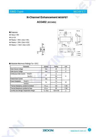
SMD Type IC SMD Type MOSFET N-Channel Enhancement MOSFET AO3402 (KO3402) SOT-23-3 Unit mm +0.2 2.9 -0.1 Features +0.1 0.4 -0.1 VDS (V) = 30V 3 ID = 4 A RDS(ON) 55m (VGS = 10V) RDS(ON) 70m (VGS = 4.5V) 1 2 +0.02 +0.1 0.15 -0.02 D 0.95 -0.1 RDS(ON) 110m (VGS = 2.5V) +0.1 1.9 -0.2 1. Gate G 2. Source S 3. Drain Absolute Maximum Ratings Ta = 25 Parameter Symbol Rating
ao3407a.pdf
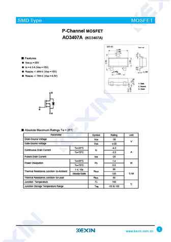
SMD Type MOSFET P-Channel MOSFET AO3407A (KO3407A) SOT-23 Unit mm 2.9+0.1 -0.1 +0.1 0.4-0.1 3 Features VDS (V) =-30V ID =-4.3 A (VGS =-10V) 1 2 +0.1 +0.05 0.95 -0.1 RDS(ON) 48m (VGS =-10V) 0.1 -0.01 +0.1 1.9 -0.1 RDS(ON) 78m (VGS =-4.5V) 1. Gate 2. Source 3. Drain D D G G S S Absolute Maximum Ratings Ta = 25 Parameter Sy
ao3409-3.pdf

SMD Type MOSFET P-Channel Enhancement MOSFET AO3409 (KO3409) SOT-23-3 Unit mm +0.2 2.9-0.1 +0.1 0.4 -0.1 Features 3 VDS (V) = -30V ID = -2.6 A (VGS = -10V) RDS(ON)
ao3404 ko3404.pdf
SMD Type IC SMD Type MOSFET N-Channel Enhancement MOSFET AO3404 (KO3404) 3 Features VDS (V) = 30V ID =5.8 A (VGS=10V) 12 RDS(ON) 28 m (VGS =10V) RDS(ON) 43 m (VGS =4.5V) D G S Absolute Maximum Ratings Ta = 25 Parameter Symbol Rating Unit Drain-Source V
ao3404a-3.pdf
SMD Type MOSFET N-Channel MOSFET AO3404A (KO3404A) SOT-23-3 Unit mm +0.2 2.9 -0.1 +0.1 0.4-0.1 3 Features VDS (V) = 30V ID = 5.8 A (VGS = 10V) 1 2 RDS(ON) 25m (VGS = 10V) +0.02 +0.1 0.15 -0.02 0.95 -0.1 +0.1 RDS(ON) 35m (VGS = 4.5V) 1.9 -0.2 D 1. Gate 2. Source 3. Drain G S Absolute Maximum Ratings Ta = 25 Parameter Symbol
ao3404.pdf
SMD Type IC SMD Type MOSFET N-Channel Enhancement MOSFET AO3404 (KO3404) SOT-23 Unit mm +0.1 2.9 -0.1 +0.1 0.4 -0.1 Features 3 VDS (V) = 30V ID =5.8 A (VGS=10V) RDS(ON) 28 m (VGS = 10V) 1 2 +0.1 +0.05 0.95 -0.1 D 0.1 -0.01 RDS(ON) 43 m (VGS = 4.5V) +0.1 1.9 -0.1 1.Base 1. Gate 2.Emitter 2. Source G 3. Drain 3.collector S Absolute Maximum Ratings Ta = 25 Paramet
ao3401a-3.pdf

SMD Type MOSFET P-Channel MOSFET AO3401A (KO3401A) SOT-23-3 Unit mm +0.2 2.9 -0.1 +0.1 0.4-0.1 3 Features VDS (V) =-30V ID =-4 A (VGS =-10V) 1 2 RDS(ON) 50m (VGS =-10V) +0.02 +0.1 0.15 -0.02 0.95 -0.1 +0.1 RDS(ON) 60m (VGS =-4.5V) 1.9 -0.2 RDS(ON) 85m (VGS =-2.5V) 1. Gate 2. Source D 3. Drain G S Absolute Maximum R
ao3400a-3.pdf
SMD Type MOSFET N-Channel MOSFET AO3400A (KO3400A) SOT-23-3 Unit mm +0.2 2.9 -0.1 +0.1 0.4-0.1 3 Features VDS (V) = 30V ID = 5.7 A (VGS = 10V) RDS(ON) 26.5m (VGS = 10V) 1 2 +0.02 +0.1 0.15 -0.02 0.95 -0.1 RDS(ON) 32m (VGS = 4.5V) +0.1 1.9 -0.2 RDS(ON) 48m (VGS = 2.5V) 1. Gate 2. Source D D 3. Drain G G S S Absol
ao3407hf.pdf
SMD Type IC SMD Type MOSFET P-Channel Enhancement MOSFET AO3407 HF (KO3407 HF) SOT-23-3 Unit mm +0.2 2.9-0.1 +0.1 0.4 -0.1 3 Features VDS (V) = -30V ID = -4.1 A 1 2 +0.02 +0.1 0.15 -0.02 RDS(ON) 52m (VGS = -10V) 0.95 -0.1 D 1.9+0.1 -0.2 RDS(ON) 87m (VGS = -4.5V) 1. Gate 2. Source G 3. Drain S Absolute Maximum Ratings Ta = 25 Parameter Symbol Rating Unit Drain-
ao3407-3.pdf
SMD Type IC SMD Type MOSFET P-Channel Enhancement MOSFET AO3407 (KO3407) SOT-23-3 Unit mm +0.2 2.9-0.1 +0.1 0.4 -0.1 3 Features VDS (V) = -30V ID = -4.1 A 1 2 +0.02 +0.1 0.15 -0.02 RDS(ON) 52m (VGS = -10V) 0.95 -0.1 D 1.9+0.1 -0.2 RDS(ON) 87m (VGS = -4.5V) 1. Gate 2. Source G 3. Drain S Absolute Maximum Ratings Ta = 25 Parameter Symbol Rating Unit Drain-Sourc
ao3404a.pdf
SMD Type MOSFET N-Channel MOSFET AO3404A (KO3404A) SOT-23 Unit mm +0.1 2.9 -0.1 +0.1 0.4-0.1 3 Features VDS (V) = 30V ID = 5.8 A (VGS = 10V) 1 2 +0.1 +0.05 RDS(ON) 25m (VGS = 10V) 0.95 -0.1 0.1 -0.01 +0.1 1.9 -0.1 RDS(ON) 35m (VGS = 4.5V) 1. Gate D 2. Source 3. Drain G S Absolute Maximum Ratings Ta = 25 Parameter Symbol Rat
ko3402 ao3402.pdf
SMD Type IC SMD Type MOSFET N-Channel Enhancement Mode Field Effect Transistor KO3402(AO3402) SOT-23 Unit mm +0.1 2.9-0.1 +0.1 0.4-0.1 3 Features VDS (V) = 30V ID =4A 12 +0.1 +0.05 RDS(ON) 55m (VGS = 10V) 0.95-0.1 0.1-0.01 +0.1 1.9-0.1 RDS(ON) 70m (VGS =4.5V) RDS(ON) 110m (VGS =2.5V) 1.Base 1. Gate 2.Emitter 2. Source 3. Drain 3.collector Absolute Maximum Ratings T
ao3400.pdf
SMD Type IC SMD Type MOSFET N-Channel Enhancement Mode Field Effect Transistor AO3400 (KO3400) SOT-23 Unit mm +0.1 Features 2.9 -0.1 +0.1 0.4 -0.1 VDS (V) = 30V 3 ID = 5.8 A (VGS = 10V) RDS(ON) 28m (VGS = 10V) 1 2 RDS(ON) 33m (VGS = 4.5V) +0.1 +0.05 0.95 -0.1 0.1 -0.01 +0.1 1.9 -0.1 RDS(ON) 52m (VGS = 2.5V) 1.Base 1. Gate 2.Emitter 2. Source 3. Drain 3.collector Ab
ao3407g.pdf
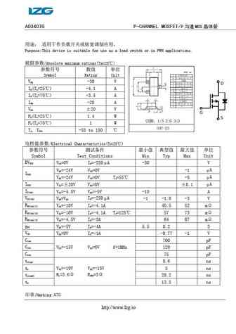
AO3407G P-CHANNEL MOSFET/P MOS Purpose This device is suitable for use as a load switch or in PWM applications. /Absolute maximum ratings(Ta=25 ) Symbol Rating Unit V -30 V DS I (T =25 ) -4.1 A D a I (T =70 ) -3.5 A D a I -20 A DM V 20 V GS P (
ao3400a.pdf
R UMW UMW AO3400A UMW AO3400A N-Channel Enhancement Mode Features SOT 23 VDS (V) = 30V ID = 5.8 A (VGS = 10V) RDS(ON) 28m (VGS = 10V) RDS(ON) 33m (VGS = 4.5V) RDS(ON) 52m (VGS = 2.5V) 1. GATE 2. SOURCE 3. DRAIN Absolute Maximum Ratings Ta = 25 Parameter Symbol Rating Unit Drain-Source Voltage VDS 30 V Gate-Source Voltage VGS 12 V Continuous Drain Current TA=25 5.8 ID
ao3409a.pdf
R UMW UMW AO3409A UMW AO3409A Features SOT 23 VDS (V) = -30V ID = -2.6 A (VGS = -10V) RDS(ON)
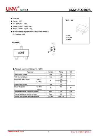
ao3401a.pdf
R UMWpe UMW AO3401A UMW AO3401A M SFET SMD Ty P-Channel Enhancement MOSFET SOT 23 Features VDS (V) =-30V ID =-4.2 A (VGS =-10V) RDS(ON) 55m (VGS =-10V) RDS(ON) 70m (VGS =-4.5V) RDS(ON) 120m (VGS =-2.5V) 1. GATE 2. SOURCE 3. DRAIN D G S Absolute Maximum Ratings Ta = 25 Parameter Symbol Rating Unit Drain-Source Voltage V
ao3407a.pdf
R UMW UMW AO3407A UMW AO3407A UMW AO3407A P-Channel Enhancement MOSFET Features SOT 23 VDS (V) = -30V ID = -4.1 A RDS(ON) 52m (VGS = -10V) RDS(ON) 87m (VGS = -4.5V) 1. GATE 2. SOURCE D 3. DRAIN G S Absolute Maximum Ratings Ta = 25 Parameter Symbol Rating Unit Drain-Source Voltage VDS -30 V Gate-Source Voltage VGS 20 Continuous Drain Current Ta = 25 -4.1
ao3402a.pdf
R UMW UMW AO3402A N-Channel MOSFET UMW AO3402A ID V(BR)DSS RDS(on)MAX SOT-23 55 m @10V 30V 4A m 70 @4.5V 110m @2.5V DESCRIPTION 1. GATE The 3402 uses advanced trench technology to provide excellent 2. SOURCE 3. DRAIN RDS(ON) , low gate charge and operation with gate voltage as low as 2.5V. This device is suitable for use as a load switch or in PWM applicat
ao3404a.pdf
R UMW UMW AO3404A UMW AO3404A UMW AO3404A N-Channel Enhancement MOSFET SOT 23 Features VDS (V) = 30V ID =5.8 A (VGS=10V) RDS(ON) 28 m (VGS = 10V) RDS(ON) 43 m (VGS = 4.5V) 1. GATE 2. SOURCE MARKING 3. DRAIN D A49T G S Absolute Maximum Ratings Ta = 25 Parameter Symbol Rating Unit Drain-Source Voltage VDS 30 V Gate-Source Voltage VGS 20 Ta=25 5.8 Continuou
ao3400a.pdf
AO3400A MOSFET ROHS N-Channel Enhancement-Mode MOSFET SOT-23 - Features Advanced trench process technology High Density Cell Design For Ultra Low On-Resistance MAXIMUM RANTINGS Characteristic Symbol Max Unit Drain-Source Voltage BV 30 V DSS Gate- Source Voltage V +12 V GS Drain Current (continuous) 5.8 A I D Drain Current (pulsed) I 30 A DM Total Device Dissipat
ao3401a.pdf
AO3401A MOSFET ROHS P-Channel Enhancement-Mode MOSFET SOT-23 - Features Advanced trench process technology High Density Cell Design For Ultra Low On-Resistance MAXIMUM RANTINGS Characteristic Symbol Max Unit -30 Drain-Source Voltage BV V DSS Gate- Source Voltage V V GS +12 Drain Current (continuous) I -4.2 A D Drain Current (pulsed) I A DM -18 Total Device D
ao3407.pdf
Plastic-Encapsulate Mosfets AO3407 FEATURES P-Channel MOSFET The AO3407 uses advanced trench technology to provide excellent RDS(ON) and low gate charge. This device is suitable for use as a load switch or in PWM applications. D D 1.Gate 2.Source SOT-23 G G 3.Drain S S Absolute Maximum Ratings (TA=25oC, unless otherwise noted) Parameter Symbol Value Unit Drain-Source Voltage
ao3402.pdf
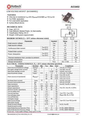
AO3402 LOW VOLTAGE MOSFET (N-CHANNEL) FEATURES Ultra low on-resistance V =30V,R 52m @V =10V,I =4A DS DS(ON) GS D For PWM application For Load switch application Surface Mount device SOT-23 MECHANICAL DATA Case SOT-23 Case Material Molded Plastic. UL flammability Classification Rating 94V-0 Weight 0.008 grams (approximate) MAXIMUM RATINGS (T
ao3401.pdf
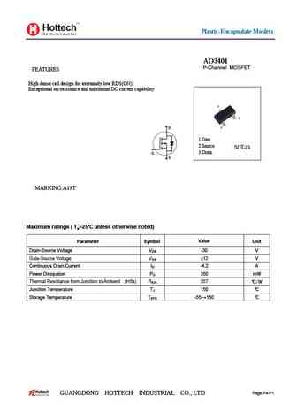
Plastic-Encapsulate Mosfets AO3401 P-Channel MOSFET FEATURES High dense cell design for extremely low RDS(ON). Exceptional on-resistance and maximum DC current capability D 1.Gate 2.Source SOT-23 3.Drain G S MARKING A19T Maximum ratings ( Ta=25 unless otherwise noted) Unit Parameter Symbol Value Drain-Source Voltage VDS -30 V Gate-Source Voltage VGS 12 V Continuous
ao3404.pdf
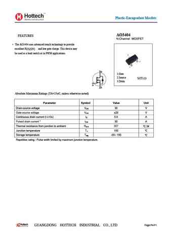
Plastic-Encapsulate Mosfets AO3404 FEATURES N-Channel MOSFET The AO3404 uses advanced trench technology to provide excellent RDS(ON) and low gate charge. This device may be used as a load switch or in PWM applications. D D 1.Gate 2.Source SOT-23 3.Drain G G S S Absolute Maximum Ratings (TA=25oC, unless otherwise noted) Parameter Symbol Value Unit Drain-source voltage VDS 3
ao3400.pdf
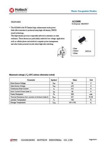
Plastic-Encapsulate Mosfets AO3400 FEATURES N-Channel MOSFET The AO3400 is the N-Channel logic enhancement mode power field effect transistor is produced using high cell density, DMOS trench technology. This high-density process is especially tailored to minimize on-state resistance. These devices are particularly suited for low voltage application such as cellular phone and notebook c
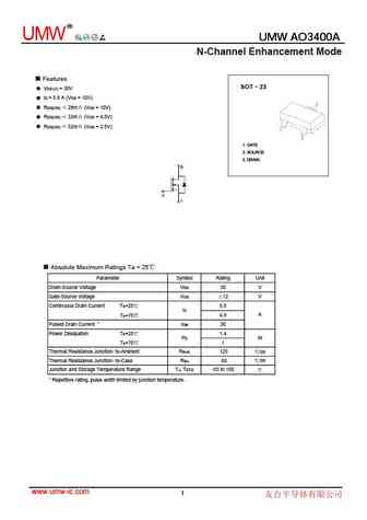
ao3400a.pdf
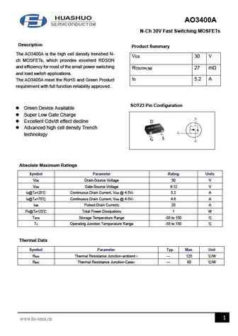
AO3400A N-Ch 30V Fast Switching MOSFETs Description Product Summary The AO3400A is the high cell density trenched N- VDS 30 V ch MOSFETs, which provides excellent RDSON and efficiency for most of the small power switching RDS(ON),typ 27 m and load switch applications. ID 5.2 A The AO3400A meet the RoHS and Green Product requirement with full function reliability approve
ao3401a.pdf
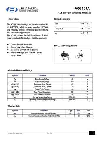
AO3401A P-Ch 30V Fast Switching MOSFETs Description Product Summary VDS -30 V The AO3401A is the high cell density trenched P- ch MOSFETs, which provides excellent RDSON RDS(ON),typ 54 m and efficiency for most of the small power switching and load switch applications. ID -4.2 A The AO3401A meet the RoHS and Green Product requirement with full function reliability approv
ao3407a.pdf
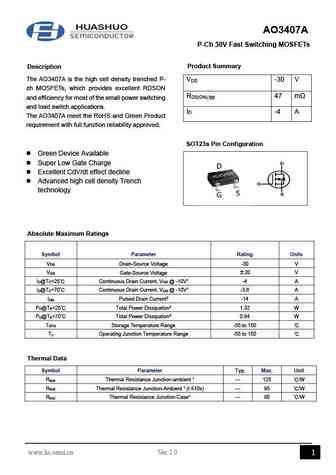
AO3407A P-Ch 30V Fast Switching MOSFETs Product Summary Description The AO3407A is the high cell density trenched P- V -30 V DS ch MOSFETs, which provides excellent RDSON R 47 m DS(ON),typ and efficiency for most of the small power switching and load switch applications. I -4 A D The AO3407A meet the RoHS and Green Product requirement with full function reliability a
ao3407.pdf
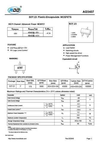
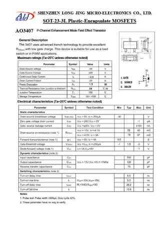
AO3407 SOT-23 Plastic-Encapsulate MOSFETS SOT-23 30V P-Channel Advanced Power MOSFET 3 ID Max V(BR)DSS RDS(on)Typ 43m @ -10V 1. GATE - 4.1A -30V 2. SOURCE 66m @ -4.5V 1 3. DRAIN 2 FEATURE APPLICATION Low RDS(on) @VGS=-10V Load Switch -5V Logic Level Control Switching circuits High-speed line driver Power Management Functions M
ao3402.pdf
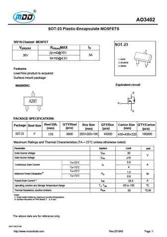
AO3402 SOT-23 Plastic-Encapsulate MOSFETS 30V N-Channel MOSFET SOT-23 ID V(BR)DSS RDS(on)MAX 3 m @10V 28 5A 30V m 34 @4.5V 1. GATE 2. SOURCE 1 3. DRAIN 2 Features Lead free product is acquired Surface mount package Equivalent circuit MARKING D A29T G S PACKAGE SPECIFICATIONS Reel DIA. Q'TY/Reel Box Size QTY/Box Carton Size Q'TY/Carton Package Reel
ao3401.pdf
AO3401 SOT-23 Plastic-Encapsulate MOSFETS SOT-23 30V P-Channel MOSFET 3 ID Max V(BR)DSS RDS(on)Typ 44m @-10V 1. GATE -4.2A -30V 2. SOURCE 51m @4.5V 1 3. DRAIN 2 FEATURE APPLICATION Load/Power Switching High dense cell design for extremely low RDS(ON) Interfacing Switching Exceptional on-resistance and maximum DC current capability MARKING Equivalen
ao3400mi-ms.pdf

www.msksemi.com AO3400MI-MS Semiconductor Compiance SOT-23 FEATURE High dense cell design for extremely low R DS(ON) Exceptional on-resistance and maximum DC current capability 1. GATE 2. SOURCE APPLICATION 3. DRAIN Load/Power Switching Interfacing Switching Equivalent Circuit I V(BR)DSS RDS(on)MAX D 35m @ 10V 40m @4.5V 30 V 5.8A 52m @2.5V Maximum ratin
ao3401mi-ms.pdf
www.msksemi.com AO3401MI-MS Semiconductor Compiance FEATURE SOT-23-3 3 High dense cell design for extremely low R . DS(ON) Exceptional on-resistance and maximum DC currentcapability 1. GATE 1 2 APPLICATION 2. SOURCE Load/Power Switching 3. DRAIN Interfacing Switching Equivalent Circuit I V(BR)DSS RDS(on)MAX D 65m @-10V 75m @-4.5V -30 V -4.2A 90m @-2.5V
ao3407.pdf

AO3407 -30V P-Channel Enhancement Mode MOSFET V = -30V DS R , V DS(ON) gs@-10V, I -4.1A
ao3402.pdf
AO3402 30V N-Channel Enhancement Mode MOSFET VDS (V) = 30V ID = 4 A RDS(ON)
ao3401.pdf

AO3401 -30V P-Channel Enhancement Mode MOSFET V = -30V DS R , V DS(ON) gs@-10V, I ds@-4.2A
ao3404.pdf
AO3404 30V N-Channel Enhancement Mode MOSFET VDS= 30V RDS(ON), Vgs@10V, Ids@5.8A
ao3400.pdf
AO3400 30V N-Channel Enhancement Mode MOSFET VDS= 30V RDS(ON), Vgs@10V, Ids@5.8A
ao3407.pdf
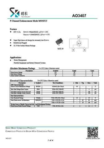
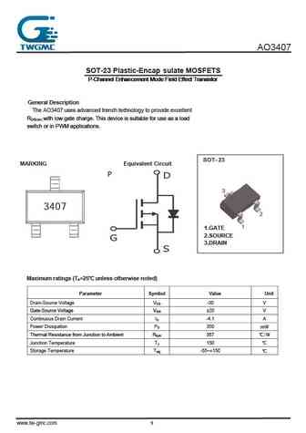
AO3407 P-Channel Enhancement Mode MOSFET Feature DS(ON) GS -30V/-4.1A, R =80m (MAX) @V = -10V. DS(ON) GS R = 100m (MAX) @V = -4.5V. . DS(ON) Super High dense cell design for extremely low R Reliable and Rugged SC-59 for Surface Mount Package SOT-59 Applications Power Management Portable Equipment and Battery Powered Systems. A T =25 Unless Ot
ao3402.pdf
AO3402 N-Channel Enhancement Mode MOSFET Feature 30V/4.2A RDS(ON) = 50m (MAX) @VGS = 10V. DS(ON) GS R =60m (MAX) @V = 4.5V. DS(ON) . Super High dense cell design for extremely low R Reliable and Rugged. for Surface Mount Package. SC-59 SC-59 A pplications Power Management Portable Equipment and Battery Powered Systems. TA=25 Unless Otherwise noted Absolute Maximum Ratin
ao3401.pdf
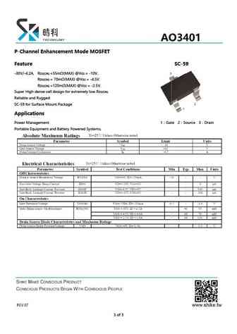
P-Channel Enhancement Mode MOSFET Channel Enhancement Mode MOSFET Feature SC-59 -30V/-4.2A, RDS(ON) =55m (MAX) @VGS = -10V. = RDS(ON) = 70m (MAX) @VGS = -4.5V. GS RDS(ON) =120m (MAX) @VGS = -2.5V. GS Super High dense cell design for extremely low R Super High dense cell design for extremely low RDS(ON) Reliable and Rugged SC-59 for Surface Mount Package Applications
ao3400.pdf
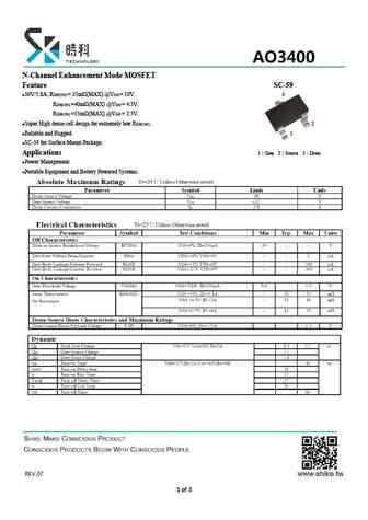
N-Channel Enhancement Mode MOSFET Feature SC-59 30V/5.8A, RDS(ON) = 35m (MAX) @VGS = 10V. 3 RDS(ON) =40m (MAX) @VGS = 4.5V. RDS(ON) =55m (MAX) @VGS = 2.5V. Super High dense cell design for extremely low RDS(ON) . 2 Reliable and Rugged. 1 SC-59 for Surface Mount Package. Applications 1 Gate 2 Source 3 Drain Power Management Portable Equipment and
ao3401.pdf
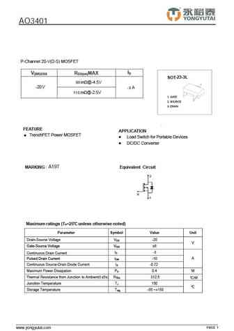
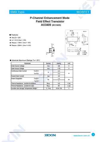
AO3401 P-Channel 20-V(D-S) MOSFET ID V(BR)DSS RDS(on)MAX SOT-23-3L 90 m @-4.5V -20V A -3 110 m @-2.5V 1. GATE 2. SOURCE 3. DRAIN FEATURE APPLICATION TrenchFET Power MOSFET z z Load Switch for Portable Devices z DC/DC Converter MARKING A19T Equivalent Circuit Maximum ratings (Ta=25 unless otherwise noted) Parameter Symbol Value Unit Drain-Source V
ao3407.pdf
SHENZHEN LONG JING MICRO-ELECTRONICS CO., LTD. SOT-23-3L Plastic-Encapsulate MOSFETS Encapsu P-Channel Enhancement Mode Field Effect Transistor A O34 0 7 Maximum ratings (Ta=25 unless otherwise noted) 4.6 1.GATE 2. SOURCE 1.5 W 3. DRAIN 84 Electrical characteristics (Ta=25 unless otherwise noted) 55 75 1.5
ao3402.pdf
SHENZHEN LONG JING MICRO-ELECTRONICS CO., LTD. SOT-23 Plastic-Encapsulate MOSFETS AO3402 N-Channel MOSFET Features RDS(on)
ao3401.pdf
SHENZHEN LONG JING MICRO-ELECTRONICS CO., LTD. SOT-23 Plastic-Encapsulate MOSFETS AO3401 P-Channel Enhancement Mode Field Effect Transistor Features V (V) = -30V DS = -4.2 A (V = -10V) ID GS R
ao3400.pdf
SHENZHEN LONG JING MICRO-ELECTRONICS CO., LTD. SOT-23 Plastic-Encapsulate Mosfets AO3400 N-Channel Mosfet Features 30V VDS 5.7A I (at VGS=10V D (at VGS=10V
ao3407.pdf
AO3407 SI2305 AO3401 SI2301 SOT-23 Plastic-Encap sulate MOSFETS P-Channel Enhancement Mode Field Effect Transistor P-Channel Enhancement Mode Field Effect Transistor P-Channel Enhancement Mode Field Effect Transistor P-Channel Enhancement Mode Field Effect Transistor P-Channel Enhancement Mode Field Effect Transistor SI2301 General Description The BC3407 uses advanced trench techno
ao3402.pdf
AO3402 AO3402 AO3402 AO3402 SOT-23 Plastic-Encapsulate MOSFETS N-Channel Enhancement Mode Field Effect Transistor N-Channel Enhancement Mode Field Effect Transistor N-Channel Enhancement Mode Field Effect Transistor N-Channel Enhancement Mode Field Effect Transistor AO3400 AO3400 AO3400 AO3400 AO3400 FEATURES APPLI
ao3401.pdf
SI2305 AO3401 AO3401 AO3401 SOT-23 Plastic-Encapsulate MOSFETS FEATURES
ao3400.pdf
AO3400 AO3400 AO3400 AO3400 SI2305 SOT-23 Plastic-Encapsulate MOSFETS N-Channel Enhancement Mode Field Effect Transistor N-Channel Enhancement Mode Field Effect Transistor N-Channel Enhancement Mode Field Effect Transistor N-Channel Enhancement Mode Field Effect Transistor AO3400 AO3400 AO3400 AO3400 AO3400 FEATURE High dense cell design for extremely low RDS(ON) Excepti
ao3407.pdf

AO3407 www.VBsemi.tw P-Channel 30 V (D-S) MOSFET FEATURES PRODUCT SUMMARY TrenchFET Power MOSFET 100 % Rg Tested VDS (V) RDS(on) ( ) Typ. ID (A)a Qg (Typ.) 0.046 at VGS = - 10 V - 5.6 0.049 at VGS = - 6 V - 5 11.4 nC - 30 APPLICATIONS 0.054 at VGS = - 4.5 V -4.5 For Mobile Computing - Load Switch - Notebook Adaptor Switch S TO-236 - DC/DC Converter (SOT-23)
ao3401.pdf
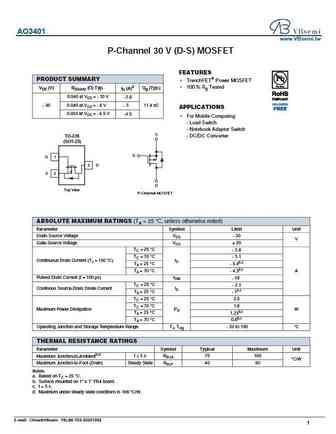
AO3401 www.VBsemi.tw P-Channel 30 V (D-S) MOSFET FEATURES PRODUCT SUMMARY TrenchFET Power MOSFET 100 % Rg Tested VDS (V) RDS(on) ( ) Typ. ID (A)a Qg (Typ.) 0.046 at VGS = - 10 V - 5.6 0.049 at VGS = - 6 V - 5 11.4 nC - 30 APPLICATIONS 0.054 at VGS = - 4.5 V -4.5 For Mobile Computing - Load Switch - Notebook Adaptor Switch S TO-236 - DC/DC Converter (SOT-23)
ao3401a.pdf

AO3401A www.VBsemi.tw P-Channel 30 V (D-S) MOSFET FEATURES PRODUCT SUMMARY TrenchFET Power MOSFET 100 % Rg Tested VDS (V) RDS(on) ( ) Typ. ID (A)a Qg (Typ.) 0.046 at VGS = - 10 V - 5.6 0.049 at VGS = - 6 V - 5 11.4 nC - 30 APPLICATIONS 0.054 at VGS = - 4.5 V -4.5 For Mobile Computing - Load Switch - Notebook Adaptor Switch S TO-236 - DC/DC Converter (SOT-23)
ao3404.pdf

AO3404 www.VBsemi.tw N-Channel 30-V (D-S) MOSFET FEATURES PRODUCT SUMMARY Halogen-free According to IEC 61249-2-21 VDS (V) RDS(on) ( ) ID (A)a Qg (Typ.) Definition 0.030 at VGS = 10 V TrenchFET Power MOSFET 6.5 30 4.5 nC 100 % Rg Tested 0.033 at VGS = 4.5 V 6.0 Compliant to RoHS Directive 2002/95/EC APPLICATIONS DC/DC Converter D TO-236 (SOT-23) G 1
ao3400.pdf
AO3400 www.VBsemi.tw N-Channel 30-V (D-S) MOSFET FEATURES PRODUCT SUMMARY Halogen-free According to IEC 61249-2-21 VDS (V) RDS(on) ( ) ID (A)a Qg (Typ.) Definition 0.030 at VGS = 10 V TrenchFET Power MOSFET 6.5 30 4.5 nC 100 % Rg Tested 0.033 at VGS = 4.5 V 6.0 Compliant to RoHS Directive 2002/95/EC APPLICATIONS DC/DC Converter D TO-236 (SOT-23) G 1
ao3401s.pdf

Description The AO3401S combines advanced trench technology to provide excellent RDS(ON), low gate charge and operation with gate voltage as low as 2.5V. This device is suitable for use as a load switch or other general applications. Features VDS= -30V, ID= -4.2A Schematic Diagram RDS(ON)typ. =45m @VDS=-10V RDS(ON)typ. =51m @VDS=-4.5V RDS(ON)typ. =65m @VDS=-2.5V Low gate
ao3400s.pdf
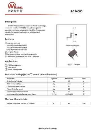
Description The AO3400S combines advanced trench technology to provide excellent RDS(ON), low gate charge and operation with gate voltage as low as 2.5V. This device is suitable for use as a load switch or other general applications. Features VDS=30V, ID=5.1A RDS(ON)
Другие MOSFET... AON6324 , SD2932 , STK1820F , STP55NE06 , STP55NE06FP , SUD50N024-06P , SVF7N65T , SVF7N65F , SPP20N60C3 , AO3407G , AO3701 , AO4420A , AO4433 , AO4456 , AO4458 , AO4474 , AO4607 .
History: 2SK845 | 2SK630 | L2N7002SWT1G | 3SK193P | WMJ25N50C4 | KX120N06 | 2N7639-GA
History: 2SK845 | 2SK630 | L2N7002SWT1G | 3SK193P | WMJ25N50C4 | KX120N06 | 2N7639-GA
🌐 : EN ES РУ

Список транзисторов
Обновления
MOSFET: ASU70R600E | ASU65R850E | ASU65R550E | ASU65R350E | ASR65R120EFD | ASR65R046EFD | ASQ65R046EFD | ASM65R280E | ASM60R330E | ASE70R950E | ASD80R750E | ASD70R950E | ASD70R600E | ASD70R380E | ASD65R850E | ASD65R550E
Popular searches
c3203 transistor | irfp450 equivalent | 2sb649 | 2sb324 transistor | b754 transistor | 2sc828 equivalent | 4843ns | 2sc1318 datasheet