AOD4112. Аналоги и основные параметры
Наименование производителя: AOD4112
Тип транзистора: MOSFET
Полярность: N
Предельные значения
Pd ⓘ - Максимальная рассеиваемая мощность: 50 W
|Vds|ⓘ - Максимально допустимое напряжение сток-исток: 30 V
|Vgs|ⓘ - Максимально допустимое напряжение затвор-исток: 20 V
|Id| ⓘ - Максимально допустимый постоянный ток стока: 20 A
Tj ⓘ - Максимальная температура канала: 175 °C
Электрические характеристики
tr ⓘ - Время нарастания: 9.3 ns
Cossⓘ - Выходная емкость: 382 pf
RDSonⓘ - Сопротивление сток-исток открытого транзистора: 0.0095 Ohm
Тип корпуса: TO252
Аналог (замена) для AOD4112
- подборⓘ MOSFET транзистора по параметрам
AOD4112 даташит
aod4112.pdf
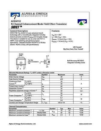
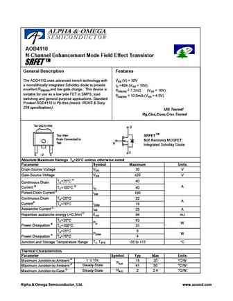
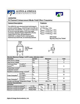
AOD4112 N-Channel Enhancement Mode Field Effect Transistor SRFET TM General Description Features SRFETTM The AOD4112 uses advanced trench technology with a monolithically integrated Schottky VDS (V) = 30V diode to provide excellent R ,and low gate charge. ID = 20A (VGS = 10V) DS(ON) This device is suitable for use as a low side FET in RDS(ON)
aod4112.pdf

AOD4112 www.VBsemi.tw N-Channel 30-V (D-S) MOSFET FEATURES PRODUCT SUMMARY TrenchFET Power MOSFET VDS (V) RDS(on) ( ) ID (A)a, e Qg (Typ) 100 % Rg and UIS Tested Compliant to RoHS Directive 2011/65/EU 0.007 at VGS = 10 V 50 30 25 nC 0.009 at VGS = 4.5 V 40 APPLICATIONS D OR-ing Server TO-252 DC/DC G G D S S Top View N-Channel MOSFET ABSOLU
aod4146.pdf
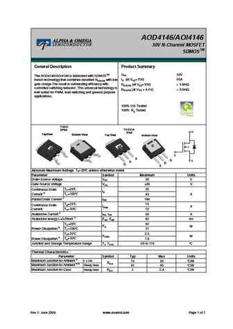
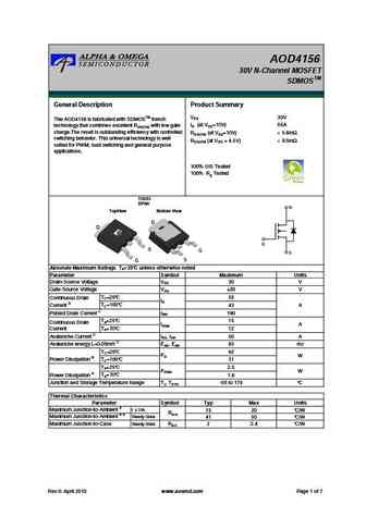
AOD4146/AOI4146 30V N-Channel MOSFET TM SDMOS General Description Product Summary 30V The AOD4146/AOI4146 is fabricated with SDMOSTM VDS ID (at VGS=10V) 55A trench technology that combines excellent RDS(ON) with low gate charge.The result is outstanding efficiency with RDS(ON) (at VGS=10V)
aod4191l.pdf
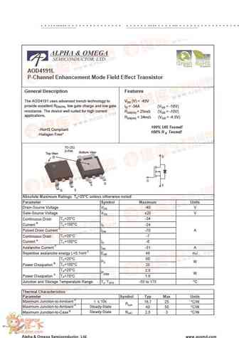
AOD4191L PCB 24 AOD4191L P-Channel Enhancement Mode Field Effect Transistor General Description Features The AOD4191 uses advanced trench technology to VDS (V) = -40V provide excellent RDS(ON), low gate charge and low gate ID = -34A (VGS = -10V) resistance. The device well suited for high current RDS(ON)
aod4185 aoi4185.pdf

AOD4185/AOI4185 P-Channel Enhancement Mode Field Effect Transistor General Description Features The AOD4185/AOI4185 uses advanced trench VDS (V) = -40V technology to provide excellent RDS(ON) and low gate ID = -40A (VGS = -10V) charge. With the excellent thermal resistance of the RDS(ON)
aod417.pdf
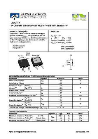
AOD417 P-Channel Enhancement Mode Field Effect Transistor General Description Features The AOD417 uses advanced trench technology to provide excellent RDS(ON), low gate charge and low VDS (V) = -30V gate resistance. With the excellent thermal resistance ID = -25A (VGS = -10V) of the DPAK package, this device is well suited for RDS(ON)
aod4130 aoi4130.pdf
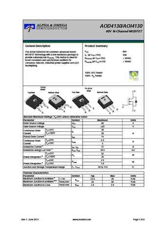
AOD4130/AOI4130 60V N-Channel MOSFET General Description Product Summary VDS 60V The AOD4130/AOI4130 combines advanced trench MOSFET technology with a low resistance package to ID (at VGS=10V) 30A provide extremely low RDS(ON). This device is ideal for RDS(ON) (at VGS=10V)
aod4189.pdf
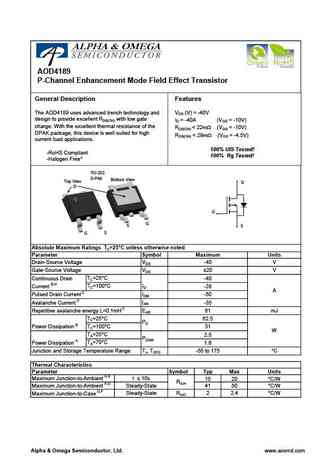
AOD4189 P-Channel Enhancement Mode Field Effect Transistor General Description Features The AOD4189 uses advanced trench technology and VDS (V) = -40V design to provide excellent RDS(ON) with low gate ID = -40A (VGS = -10V) charge. With the excellent thermal resistance of the RDS(ON)
aod410.pdf
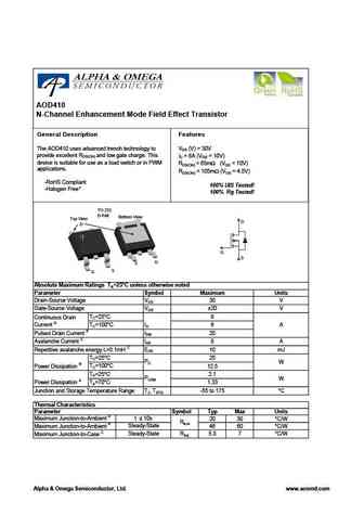
AOD410 N-Channel Enhancement Mode Field Effect Transistor General Description Features The AOD410 uses advanced trench technology to VDS (V) = 30V provide excellent RDS(ON) and low gate charge. This ID = 8A (VGS = 10V) device is suitable for use as a load switch or in PWM RDS(ON)
aod4126.pdf

AOD4126/AOI4126 100V N-Channel MOSFET TM SDMOS General Description Product Summary 100V The AOD4126&AOI4126 are fabricated with SDMOSTM VDS ID (at VGS=10V) 43A trench technology that combines excellent RDS(ON) with low gate charge.The result is outstanding efficiency with RDS(ON) (at VGS=10V)
aod413a.pdf
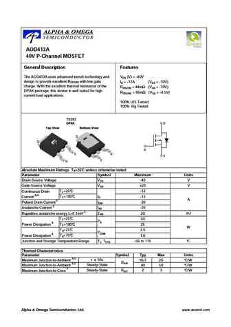
AOD413A 40V P-Channel MOSFET General Description Features The AOD413A uses advanced trench technology and VDS (V) = -40V design to provide excellent RDS(ON) with low gate ID = -12A (VGS = -10V) charge. With the excellent thermal resistance of the RDS(ON)
aod4102.pdf
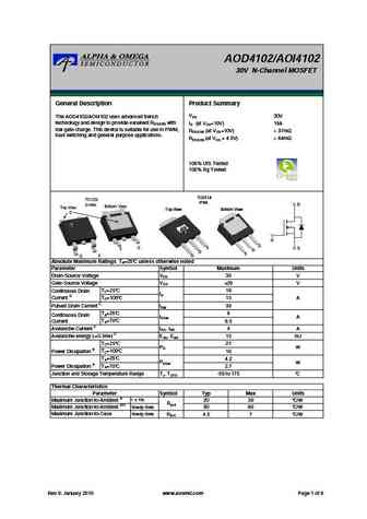
AOD4102/AOI4102 30V N-Channel MOSFET General Description Product Summary VDS 30V The AOD4102/AOI4102 uses advanced trench technology and design to provide excellent RDS(ON) with ID (at VGS=10V) 19A low gate charge. This device is suitable for use in PWM, RDS(ON) (at VGS=10V)
aod4128.pdf
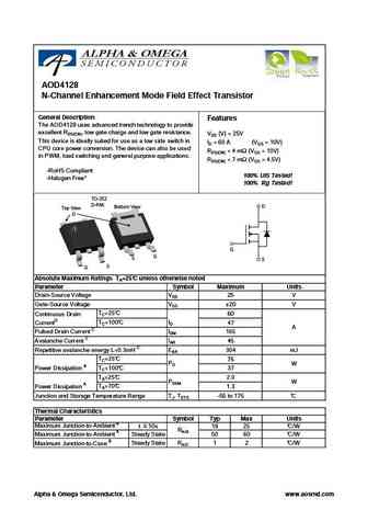
AOD4128 N-Channel Enhancement Mode Field Effect Transistor General Description Features The AOD4128 uses advanced trench technology to provide excellent RDS(ON), low gate charge and low gate resistance. VDS (V) = 25V This device is ideally suited for use as a low side switch in ID = 60 A (VGS = 10V) CPU core power conversion. The device can also be used RDS(ON)
aod4185.pdf

AOD4185/AOI4185 P-Channel Enhancement Mode Field Effect Transistor General Description Features The AOD4185/AOI4185 uses advanced trench VDS (V) = -40V technology to provide excellent RDS(ON) and low gate ID = -40A (VGS = -10V) charge. With the excellent thermal resistance of the RDS(ON)
aod4144.pdf
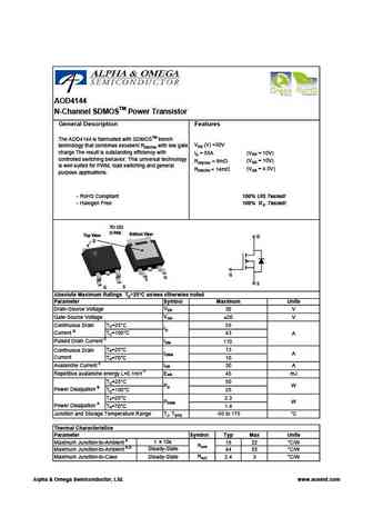
AOD4144 N-Channel SDMOSTM Power Transistor General Description Features The AOD4144 is fabricated with SDMOSTM trench VDS (V) =30V technology that combines excellent RDS(ON) with low gate charge.The result is outstanding efficiency with (VGS = 10V) ID = 55A controlled switching behavior. This universal technology (VGS = 10V) RDS(ON)
aod4184.pdf
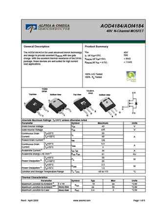
AOD4184/AOI4184 40V N-Channel MOSFET General Description Product Summary VDS The AOD4184/AOI4184 used advanced trench technology 40V 50A and design to provide excellent RDS(ON) with low gate ID (at VGS=10V) charge. With the excellent thermal resistance of the DPAK
aod4132.pdf
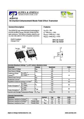
AOD4132 N-Channel Enhancement Mode Field Effect Transistor General Description Features The AOD4132 uses advanced trench technology to VDS (V) = 30V provide excellent RDS(ON), low gate charge and low ID = 85A (VGS = 10V) gate resistance. This device is ideally suited for use RDS(ON)
aod4124.pdf
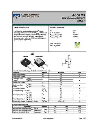
AOD4124 100V N-Channel MOSFET TM SDMOS General Description Product Summary VDS 100V The AOD4124 is fabricated with SDMOSTM trench 54A ID (at VGS=10V) technology that combines excellent RDS(ON) with low gate
aod4187.pdf
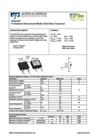
AOD4187 P-Channel Enhancement Mode Field Effect Transistor General Description Features The AOD4187 uses advanced trench technology and VDS (V) = -40V design to provide excellent RDS(ON) with low gate charge. ID = -45A (VGS = -10V) With the excellent thermal resistance of the DPAK RDS(ON)
aod4184a.pdf
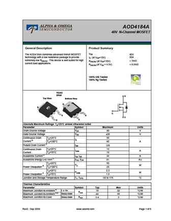
AOD4184A 40V N-Channel MOSFET General Description Product Summary VDS The AOD4184A combines advanced trench MOSFET 40V 50A technology with a low resistance package to provide ID (at VGS=10V) extremely low RDS(ON). This device is well suited for high
aod4182.pdf
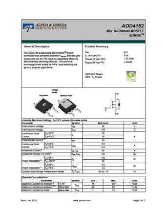
AOD4182 80V N-Channel MOSFET TM SDMOS General Description Product Summary VDS 80V The AOD4182 is fabricated with SDMOSTM trench ID (at VGS=10V) 53A technology that combines excellent RDS(ON) with low gate
aod4180.pdf

AOD4180 80V N-Channel MOSFET TM SDMOS General Description Product Summary VDS 80V The AOD4180 is fabricated with SDMOSTM trench 54A ID (at VGS=10V) technology that combines excellent RDS(ON) with low gate
aod4100.pdf
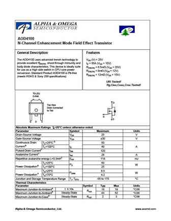
AOD4100 N-Channel Enhancement Mode Field Effect Transistor General Description Features The AOD4100 uses advanced trench technology to VDS (V) = 25V provide excellent RDS(ON), shoot-through immunity and ID = 50A (VGS = 10V) body diode characteristics. This device is ideally suite RDS(ON)
aod414.pdf
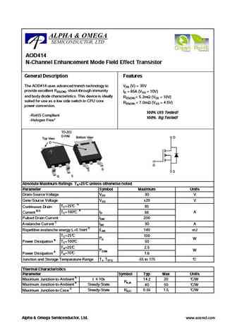
AOD414 N-Channel Enhancement Mode Field Effect Transistor General Description Features The AOD414 uses advanced trench technology to VDS (V) = 30V provide excellent RDS(ON), shoot-through immunity ID = 85A (VGS = 10V) and body diode characteristics. This device is ideally RDS(ON)
aod4120.pdf
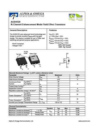
AOD4120 N-Channel Enhancement Mode Field Effect Transistor 1.4 General Description Features The AOD4120 uses advanced trench technology and VDS (V) = 20V design to provide excellent RDS(ON) with low gate ID = 25A (VGS = 10V) charge. This device is suitable for use in PWM, load RDS(ON)
aod4136.pdf
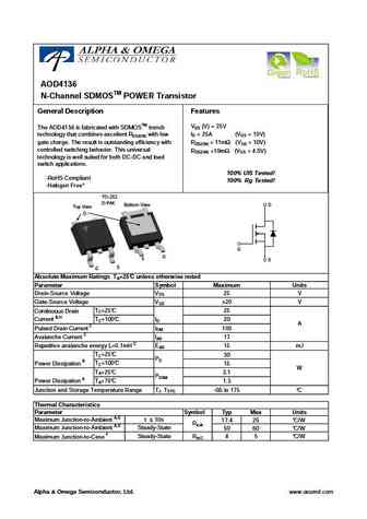
AOD4136 N-Channel SDMOSTM POWER Transistor General Description Features VDS (V) = 25V The AOD4136 is fabricated with SDMOSTM trench ID = 25A (VGS = 10V) technology that combines excellent RDS(ON) with low gate charge. The result is outstanding efficiency with RDS(ON)
aod4130.pdf

AOD4130/AOI4130 60V N-Channel MOSFET General Description Product Summary VDS 60V The AOD4130/AOI4130 combines advanced trench MOSFET technology with a low resistance package to ID (at VGS=10V) 30A provide extremely low RDS(ON). This device is ideal for RDS(ON) (at VGS=10V)
aod4186.pdf
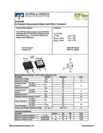
AOD4186 N-Channel Enhancement Mode Field Effect Transistor General Description Features The AOD4186 combines advanced trench MOSFET technology with a low resistance package to provide VDS (V) =40V extremely low RDS(ON). This device is ideal for low (VGS = 10V) ID = 35A voltage inverter applications. (VGS = 10V) RDS(ON)
aod4104.pdf
AOD4104 N-Channel Enhancement Mode Field Effect Transistor General Description Features The AOD4104 uses advanced trench technology to VDS (V) = 25V provide excellent RDS(ON), shoot-through immunity and ID = 75A (VGS = 10V) body diode characteristics. This device is ideally suite RDS(ON)
aod4106.pdf
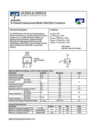
AOD4106 N-Channel Enhancement Mode Field Effect Transistor General Description Features The AOD4106 uses advanced trench technology to VDS (V) = 25V provide excellent RDS(ON), low gate charge.This device is ID = 50A (VGS = 20V) suitable for use as a low side switch in SMPS and RDS(ON)
aod4126 aoi4126.pdf
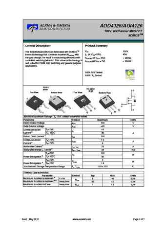
AOD4126/AOI4126 100V N-Channel MOSFET TM SDMOS General Description Product Summary 100V The AOD4126&AOI4126 are fabricated with SDMOSTM VDS ID (at VGS=10V) 43A trench technology that combines excellent RDS(ON) with low gate charge.The result is outstanding efficiency with RDS(ON) (at VGS=10V)
aod4184 aoi4184.pdf

AOD4184/AOI4184 40V N-Channel MOSFET General Description Product Summary VDS 40V The AOD4184/AOI4184 used advanced trench technology and design to provide excellent RDS(ON) with ID (at VGS=10V) 50A low gate charge. With the excellent thermal resistance of RDS(ON) (at VGS=10V)
aod418.pdf
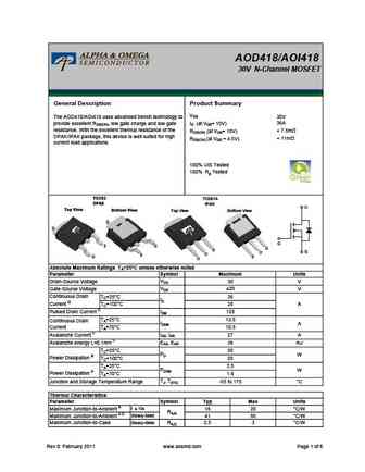
AOD418/AOI418 30V N-Channel MOSFET General Description Product Summary VDS The AOD418/AOI418 uses advanced trench technology to 30V 36A provide excellent RDS(ON), low gate charge and low gate ID (at VGS= 10V) resistance. With the excellent thermal resistance of the
aob413 aod413.pdf
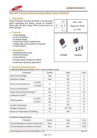
AOB413/AOD413 30A 40V P-channel Enhancement Mode Power MOSFET 1 Description These P-channel enhanced vdmosfets, used advanced V = -40V DSS trench technology and design, provide to excellent Rdson with low gate charge. Which accords with the R = 30m DS(on) (TYP) RoHS standard. I = -30A D 2 Features Fast switching Low on resistance Low gate charge Low reverse tr
aod413.pdf
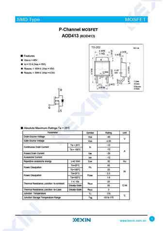
SMD Type MOSFET P-Channel MOSFET AOD413 (KOD413) TO-252 Unit mm 6.50+0.15 -0.15 +0.1 2.30 -0.1 +0.2 5.30-0.2 +0.8 0.50 -0.7 Features 4 VDS (V) =-40V ID =-12 A (VGS =-10V) RDS(ON) 45m (VGS =-10V) 0.127 0.80+0.1 max -0.1 RDS(ON) 69m (VGS =-4.5V) 1 Gate 2 Drain 2.3 0.60+ 0.1 - 0.1 3 Source +0.15 4.60 -0.15 4 Drain D G S Absol
aod417.pdf
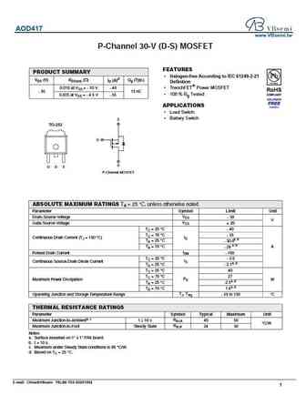
AOD417 www.VBsemi.tw P-Channel 30-V (D-S) MOSFET FEATURES PRODUCT SUMMARY Halogen-free According to IEC 61249-2-21 VDS (V) RDS(on) ( ) ID (A)d Qg (Typ.) Definition 0.018 at VGS = - 10 V - 40 TrenchFET Power MOSFET - 30 13 nC 100 % Rg Tested 0.025 at VGS = - 4.5 V - 35 APPLICATIONS Load Switch Battery Switch S TO-252 G D G D S P-Channel MOSFET ABSO
aod4189.pdf
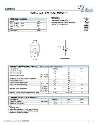
AOD4189 www.VBsemi.tw P-Channel 4 0 V (D-S) MOSFET FEATURES PRODUCT SUMMARY TrenchFET power MOSFET VDS (V) -40 Package with low thermal resistance RDS(on) ( ) at VGS = -10 V 0.012 100 % Rg and UIS tested RDS(on) ( ) at VGS = -4.5 V 0.015 ID (A) -50 Configuration Single TO-252 S G D D G S P-Channel MOSFET Top View ABSOLUTE MAXIMUM RATINGS (TC = 25 C, unle
aod410.pdf
AOD410 www.VBsemi.tw N-Channel 30-V (D-S) MOSFET FEATURES PRODUCT SUMMARY TrenchFET Power MOSFET VDS (V) RDS(on) ( ) ID (A)a, e Qg (Typ) 100 % Rg and UIS Tested Compliant to RoHS Directive 2011/65/EU 0.007 at VGS = 10 V 50 30 25 nC 0.009 at VGS = 4.5 V 40 APPLICATIONS D OR-ing Server TO-252 DC/DC G G D S S Top View N-Channel MOSFET ABSOLUT
aod4185.pdf

AOD4185 www.VBsemi.tw P-Channel 4 0 V (D-S) MOSFET FEATURES PRODUCT SUMMARY TrenchFET power MOSFET VDS (V) -40 Package with low thermal resistance RDS(on) ( ) at VGS = -10 V 0.012 100 % Rg and UIS tested RDS(on) ( ) at VGS = -4.5 V 0.015 ID (A) -50 Configuration Single TO-252 S G D D G S P-Channel MOSFET Top View ABSOLUTE MAXIMUM RATINGS (TC = 25 C, unle
aod4144.pdf

AOD4144 www.VBsemi.tw N-Channel 30-V (D-S) MOSFET FEATURES PRODUCT SUMMARY TrenchFET Power MOSFET VDS (V) RDS(on) ( ) ID (A)a, e Qg (Typ) 100 % Rg and UIS Tested Compliant to RoHS Directive 2011/65/EU 0.005 at VGS = 10 V 80 30 31 nC 0.006 at VGS = 4.5 V 68 APPLICATIONS D OR-ing TO-252 Server DC/DC G G D S Top View S N-Channel MOSFET ABSOLUT
aod4184.pdf
AOD4184 www.VBsemi.tw N-Channel 40-V (D-S) MOSFET FEATURES PRODUCT SUMMARY TrenchFET Power MOSFET VDS (V) RDS(on) ( ) ID (A)a, c Qg (Typ.) 100 % Rg and UIS Tested RoHS 0.0050 at VGS = 10 V 85 COMPLIANT 40 80 nC 0.0065 at VGS = 4.5 V 70 APPLICATIONS Synchronous Rectification Power Supplies D TO-252 G G D S S N-Channel MOSFET ABSOLUTE MAXIMUM RATI
aod4132.pdf

AOD4132 www.VBsemi.tw N-Channel 30-V (D-S) MOSFET FEATURES PRODUCT SUMMARY TrenchFET Power MOSFET VDS (V) RDS(on) ( ) ID (A)a, e Qg (Typ) 100 % Rg and UIS Tested Compliant to RoHS Directive 2011/65/EU 0.002 at VGS = 10 V 100 30 72 nC 0.003 at VGS = 4.5 V 90 APPLICATIONS D OR-ing Server TO-252 DC/DC G G D S Top View S N-Channel MOSFET ABSOL
aod4180.pdf
AOD4180 www.VBsemi.tw N-Channel 80 V (D-S) MOSFET FEATURES PRODUCT SUMMARY TrenchFET Power MOSFET VDS (V) RDS(on) ( ) Max. ID (A) Qg (Typ.) 100 % Rg and UIS Tested 0.0055 at VGS = 10 V 75a 80 0.0088 at VGS = 6.0 V 65a 17.1 nC APPLICATIONS 0.0115 at VGS = 5.0 V 54 Primary Side Switching Synchronous Rectification TO-252 D DC/AC Inverters LED Backlightin
aod414.pdf
AOD414 www.VBsemi.tw N-Channel 30-V (D-S) MOSFET FEATURES PRODUCT SUMMARY TrenchFET Power MOSFET VDS (V) RDS(on) ( ) ID (A)a, e Qg (Typ) 100 % Rg and UIS Tested Compliant to RoHS Directive 2011/65/EU 0.002 at VGS = 10 V 100 30 72 nC 0.003 at VGS = 4.5 V 90 APPLICATIONS D OR-ing Server TO-252 DC/DC G G D S Top View S N-Channel MOSFET ABSOLU
aod4130.pdf
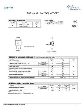
AOD4130 www.VBsemi.tw N-Channel 6 0-V (D-S) MOSFET FEATURES PRODUCT SUMMARY TrenchFET Power MOSFET VDS (V) rDS(on) ( ) ID (A)a Available 175 C Junction Temperature 0.025 at VGS = 10 V 35 RoHS* 60 0.030 at VGS = 4.5 V 30 COMPLIANT TO-252 D G Drain Connected to Tab G D S S Top View N-Channel MOSFET ABSOLUTE MAXIMUM RATINGS TC = 25 C, unless otherwise noted
aod4146.pdf

isc N-Channel MOSFET Transistor AOD4146 FEATURES Drain Current I = 55A@ T =25 D C Drain Source Voltage- V =30V(Min) DSS Static Drain-Source On-Resistance R =5.6m (Max) DS(on) 100% avalanche tested Minimum Lot-to-Lot variations for robust device performance and reliable operation DESCRIPTION Designed for use in switch mode power supplies and general purpose
aod417.pdf

isc P-Channel MOSFET Transistor AOD417 FEATURES Drain Current I =-25A@ T =25 D C Drain Source Voltage- V =-30V(Min) DSS Static Drain-Source On-Resistance R = 34m (Max) DS(on) 100% avalanche tested Minimum Lot-to-Lot variations for robust device performance and reliable operation DESCRIPTION Designed for use in switch mode power supplies and general purpose
aod4156.pdf

isc N-Channel MOSFET Transistor AOD4156 FEATURES Drain Current I = 55A@ T =25 D C Drain Source Voltage- V =30V(Min) DSS Static Drain-Source On-Resistance R =5.6m (Max) DS(on) 100% avalanche tested Minimum Lot-to-Lot variations for robust device performance and reliable operation DESCRIPTION Designed for use in switch mode power supplies and general purpose
aod4189.pdf

isc P-Channel MOSFET Transistor AOD4189 FEATURES Drain Current I = -40A@ T =25 D C Drain Source Voltage- V =-40V(Min) DSS Static Drain-Source On-Resistance R =22m (Max) DS(on) 100% avalanche tested Minimum Lot-to-Lot variations for robust device performance and reliable operation DESCRIPTION Designed for use in switch mode power supplies and general purpose
aod4126.pdf

isc N-Channel MOSFET Transistor AOD4126 FEATURES Drain Current I = 43A@ T =25 D C Drain Source Voltage- V =100V(Min) DSS Static Drain-Source On-Resistance R =24m (Max) DS(on) 100% avalanche tested Minimum Lot-to-Lot variations for robust device performance and reliable operation DESCRIPTION Designed for use in switch mode power supplies and general purpose
aod413a.pdf

isc P-Channel MOSFET Transistor AOD413A FEATURES Drain Current I = -12A@ T =25 D C Drain Source Voltage- V =-40V(Min) DSS Static Drain-Source On-Resistance R =11m (Max) DS(on) 100% avalanche tested Minimum Lot-to-Lot variations for robust device performance and reliable operation DESCRIPTION Designed for use in switch mode power supplies and general purpose
aod4102.pdf

isc N-Channel MOSFET Transistor AOD4102 FEATURES Drain Current I = 19A@ T =25 D C Drain Source Voltage- V =30V(Min) DSS Static Drain-Source On-Resistance R =37m (Max) DS(on) 100% avalanche tested Minimum Lot-to-Lot variations for robust device performance and reliable operation DESCRIPTION Designed for use in switch mode power supplies and general purpose a
aod4128.pdf
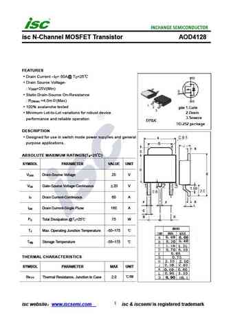
isc N-Channel MOSFET Transistor AOD4128 FEATURES Drain Current I = 60A@ T =25 D C Drain Source Voltage- V =25V(Min) DSS Static Drain-Source On-Resistance R =4.0m (Max) DS(on) 100% avalanche tested Minimum Lot-to-Lot variations for robust device performance and reliable operation DESCRIPTION Designed for use in switch mode power supplies and general purpose
aod4185.pdf
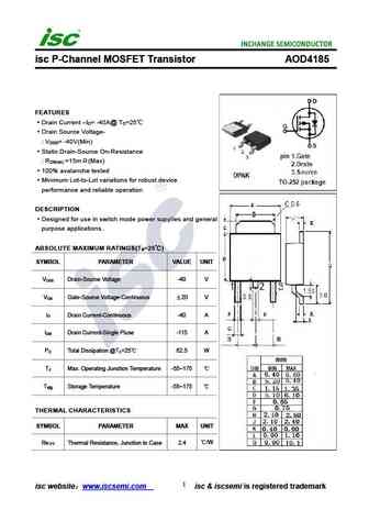
isc P-Channel MOSFET Transistor AOD4185 FEATURES Drain Current I = -40A@ T =25 D C Drain Source Voltage- V = -40V(Min) DSS Static Drain-Source On-Resistance R =15m (Max) DS(on) 100% avalanche tested Minimum Lot-to-Lot variations for robust device performance and reliable operation DESCRIPTION Designed for use in switch mode power supplies and general purpos
aod4184.pdf
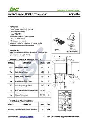
isc N-Channel MOSFET Transistor AOD4184 FEATURES Drain Current I = 50A@ T =25 D C Drain Source Voltage- V = 40V(Min) DSS Static Drain-Source On-Resistance R = 8m (Max) DS(on) 100% avalanche tested Minimum Lot-to-Lot variations for robust device performance and reliable operation DESCRITION Be suitable for synchronous rectification for server and general
aod4132.pdf

isc N-Channel MOSFET Transistor AOD4132 FEATURES Drain Current I = 85A@ T =25 D C Drain Source Voltage- V =30V(Min) DSS Static Drain-Source On-Resistance R =4.0m (Max) DS(on) 100% avalanche tested Minimum Lot-to-Lot variations for robust device performance and reliable operation DESCRIPTION Designed for use in switch mode power supplies and general purpose
aod4124.pdf
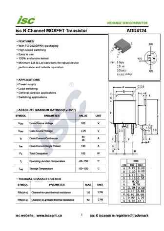
INCHANGE Semiconductor isc N-Channel MOSFET Transistor AOD4124 FEATURES With TO-252(DPAK) packaging High speed switching Easy to use 100% avalanche tested Minimum Lot-to-Lot variations for robust device performance and reliable operation APPLICATIONS Power supply Load switching General purpose applications Switching applications ABSOLUTE MAXIMUM RATINGS(T =
aod4184a.pdf

isc N-Channel MOSFET Transistor AOD4184A FEATURES Drain Current I = 50A@ T =25 D C Drain Source Voltage- V = 40V(Min) DSS Static Drain-Source On-Resistance R = 7m (Max) DS(on) 100% avalanche tested Minimum Lot-to-Lot variations for robust device performance and reliable operation DESCRITION Be suitable for synchronous rectification for server and genera
aod4182.pdf

isc N-Channel MOSFET Transistor AOD4182 FEATURES Drain Current I = 53A@ T =25 D C Drain Source Voltage- V =80V(Min) DSS Static Drain-Source On-Resistance R =15.5m (Max) DS(on) 100% avalanche tested Minimum Lot-to-Lot variations for robust device performance and reliable operation DESCRIPTION Designed for use in switch mode power supplies and general purpose
aod4180.pdf

isc N-Channel MOSFET Transistor AOD4180 FEATURES Drain Current I = 54A@ T =25 D C Drain Source Voltage- V =80V(Min) DSS Static Drain-Source On-Resistance R =14m (Max) DS(on) 100% avalanche tested Minimum Lot-to-Lot variations for robust device performance and reliable operation DESCRIPTION Designed for use in switch mode power supplies and general purpose a
aod4120.pdf

isc N-Channel MOSFET Transistor AOD4120 FEATURES Drain Current I = 25A@ T =25 D C Drain Source Voltage- V =20V(Min) DSS Static Drain-Source On-Resistance R =18m (Max) DS(on) 100% avalanche tested Minimum Lot-to-Lot variations for robust device performance and reliable operation DESCRIPTION Designed for use in switch mode power supplies and general purpose a
aod4136.pdf

isc N-Channel MOSFET Transistor AOD4136 FEATURES Drain Current I = 25A@ T =25 D C Drain Source Voltage- V =25V(Min) DSS Static Drain-Source On-Resistance R =11m (Max) DS(on) 100% avalanche tested Minimum Lot-to-Lot variations for robust device performance and reliable operation DESCRIPTION Designed for use in switch mode power supplies and general purpose a
aod4130.pdf
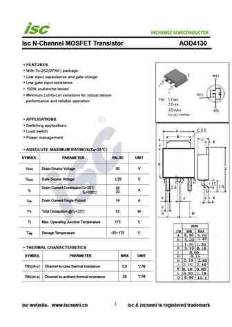
INCHANGE Semiconductor Isc N-Channel MOSFET Transistor AOD4130 FEATURES With To-252(DPAK) package Low input capacitance and gate charge Low gate input resistance 100% avalanche tested Minimum Lot-to-Lot variations for robust device performance and reliable operation APPLICATIONS Switching applications Load switch Power management ABSOLUTE MAXIMUM RATINGS(T =25
aod4186.pdf
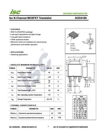
INCHANGE Semiconductor Isc N-Channel MOSFET Transistor AOD4186 FEATURES With To-252(DPAK) package Low input capacitance and gate charge Low gate input resistance 100% avalanche tested Minimum Lot-to-Lot variations for robust device performance and reliable operation APPLICATIONS Switching applications ABSOLUTE MAXIMUM RATINGS(T =25 ) a SYMBOL PARAMETER VALUE UNI
aod418.pdf
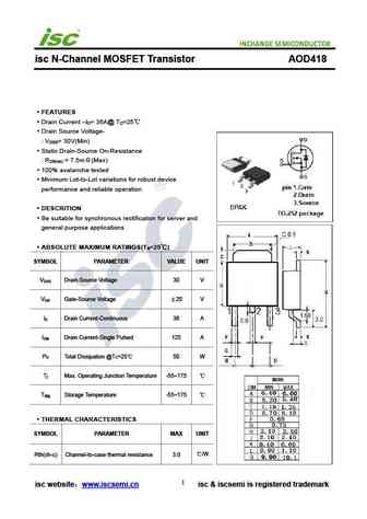
isc N-Channel MOSFET Transistor AOD418 FEATURES Drain Current I = 36A@ T =25 D C Drain Source Voltage- V = 30V(Min) DSS Static Drain-Source On-Resistance R = 7.5m (Max) DS(on) 100% avalanche tested Minimum Lot-to-Lot variations for robust device performance and reliable operation DESCRITION Be suitable for synchronous rectification for server and genera
Другие MOSFET... AOB482 , AOB4S60L , AOB7S60L , AOB7S65L , AOD4100 , AOD4104 , AOD4106 , AOD4110 , K2611 , AOI1N60L , AOI472A , AOI518 , AOK18N65L , AOK20N60L , AOK20S60L , AOK22N50L , AOK27S60L .
History: AOI1N60L | IRF8304M
🌐 : EN ES РУ

Список транзисторов
Обновления
MOSFET: ASU70R600E | ASU65R850E | ASU65R550E | ASU65R350E | ASR65R120EFD | ASR65R046EFD | ASQ65R046EFD | ASM65R280E | ASM60R330E | ASE70R950E | ASD80R750E | ASD70R950E | ASD70R600E | ASD70R380E | ASD65R850E | ASD65R550E
Popular searches
mps2907a transistor equivalent | 2sc1626 | b560 transistor | 2sc632a | c3856 | 30100 transistor | 2sc1675 | k117 transistor