AOD424G. Аналоги и основные параметры
Наименование производителя: AOD424G
Тип транзистора: MOSFET
Полярность: N
Предельные значения
Pd ⓘ
- Максимальная рассеиваемая мощность: 50 W
|Vds|ⓘ - Максимально допустимое напряжение сток-исток: 20 V
|Vgs|ⓘ - Максимально допустимое напряжение затвор-исток: 12 V
|Id| ⓘ - Максимально допустимый постоянный ток стока: 46 A
Электрические характеристики
tr ⓘ -
Время нарастания: 17 ns
Cossⓘ - Выходная емкость: 485 pf
RDSonⓘ - Сопротивление сток-исток открытого транзистора: 0.0049 Ohm
Тип корпуса: TO-252
Аналог (замена) для AOD424G
- подборⓘ MOSFET транзистора по параметрам
AOD424G даташит
..1. Size:418K aosemi
aod424g.pdf 
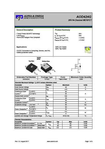
AOD424G 20V N-Channel MOSFET General Description Product Summary VDS Trench Power MOSFET technology 20V Low RDS(ON) ID (at VGS=4.5V) 46A RoHS and Halogen-Free Compliant RDS(ON) (at VGS=4.5V)
..2. Size:265K inchange semiconductor
aod424g.pdf 
isc N-Channel MOSFET Transistor AOD424G FEATURES Drain Current I = 46A@ T =25 D C Drain Source Voltage- V =20V(Min) DSS Static Drain-Source On-Resistance R = 4.9m (Max) DS(on) 100% avalanche tested Minimum Lot-to-Lot variations for robust device performance and reliable operation DESCRIPTION Designed for use in switch mode power supplies and general purpose
8.1. Size:452K aosemi
aod424.pdf 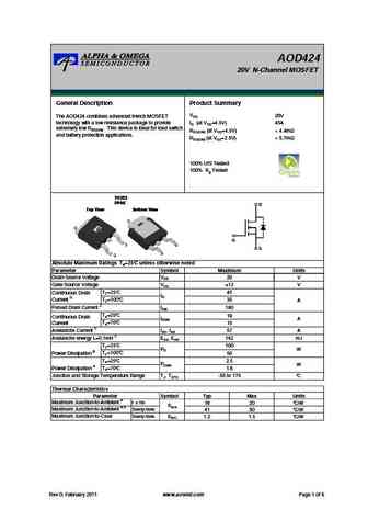
AOD424 20V N-Channel MOSFET General Description Product Summary VDS 20V The AOD424 combines advanced trench MOSFET technology with a low resistance package to provide ID (at VGS=4.5V) 45A extremely low RDS(ON). This device is ideal for load switch RDS(ON) (at VGS=4.5V)
8.2. Size:264K inchange semiconductor
aod424.pdf 
isc N-Channel MOSFET Transistor AOD424 FEATURES Drain Current I = 45A@ T =25 D C Drain Source Voltage- V =20V(Min) DSS Static Drain-Source On-Resistance R = 4.4m (Max) DS(on) 100% avalanche tested Minimum Lot-to-Lot variations for robust device performance and reliable operation DESCRIPTION Designed for use in switch mode power supplies and general purpose
9.1. Size:318K aosemi
aod4286.pdf 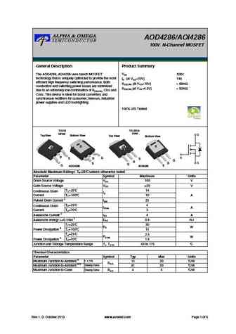
AOD4286/AOI4286 100V N-Channel MOSFET General Description Product Summary VDS 100V The AOD4286, AOI4286 uses trench MOSFET technology that is uniquely optimized to provide the most ID (at VGS=10V) 14A efficient high frequency switching performance. Both RDS(ON) (at VGS=10V)
9.2. Size:133K aosemi
aod421.pdf 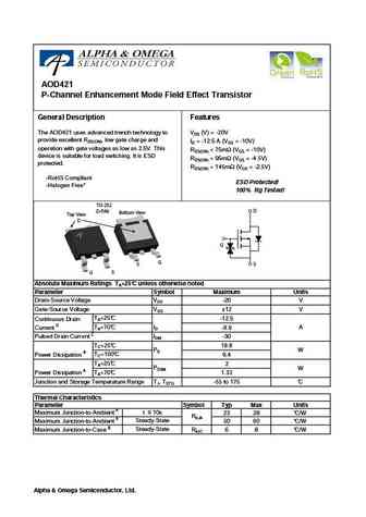
AOD421 P-Channel Enhancement Mode Field Effect Transistor General Description Features The AOD421 uses advanced trench technology to VDS (V) = -20V provide excellent RDS(ON), low gate charge and ID = -12.5 A (VGS = -10V) operation with gate voltages as low as 2.5V. This RDS(ON)
9.3. Size:566K aosemi
aod420.pdf 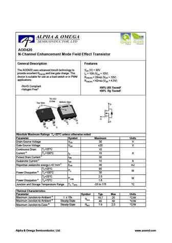
AOD420 N-Channel Enhancement Mode Field Effect Transistor General Description Features The AOD420 uses advanced trench technology to VDS (V) = 30V provide excellent RDS(ON) and low gate charge. This ID = 10A (VGS = 10V) device is suitable for use as a load switch or in PWM RDS(ON)
9.4. Size:374K aosemi
aod423.pdf 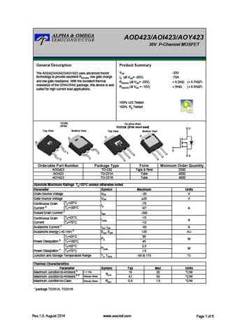
AOD423/AOI423/AOY423 30V P-Channel MOSFET General Description Product Summary VDS -30V The AOD423/AOI423/AOY423 uses advanced trench technology to provide excellent RDS(ON), low gate charge ID (at VGS= -20V) -70A and low gate resistance. With the excellent thermal RDS(ON) (at VGS= -20V)
9.5. Size:318K aosemi
aod4286 aoi4286.pdf 
AOD4286/AOI4286 100V N-Channel MOSFET General Description Product Summary VDS 100V The AOD4286, AOI4286 uses trench MOSFET technology that is uniquely optimized to provide the most ID (at VGS=10V) 14A efficient high frequency switching performance. Both RDS(ON) (at VGS=10V)
9.6. Size:459K aosemi
aod423 aoi423 aoy423.pdf 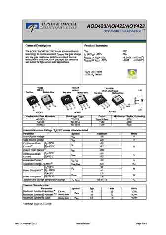
AOD423/AOI423/AOY423 TM 30V P-Channel AlphaSGT General Description Product Summary VDS -30V The AOD423/AOI423/AOY423 uses advanced trench technology to provide excellent RDS(ON), low gate charge ID (at VGS= -20V) -70A and low gate resistance. With the excellent thermal RDS(ON) (at VGS= -20V)
9.7. Size:252K aosemi
aod425.pdf 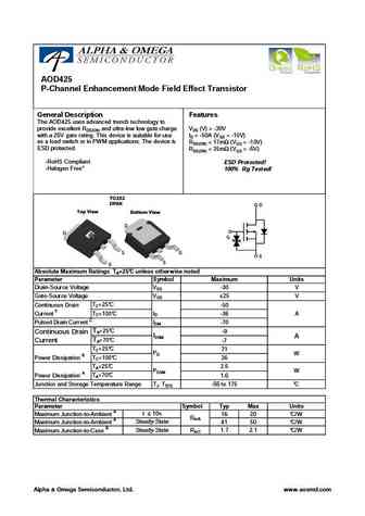
AOD425 P-Channel Enhancement Mode Field Effect Transistor General Description Features The AOD425 uses advanced trench technology to provide excellent RDS(ON) and ultra-low low gate charge VDS (V) = -30V with a 25V gate rating. This device is suitable for use ID = -50A (VGS = -10V) as a load switch or in PWM applications. The device is RDS(ON)
9.8. Size:422K aosemi
aod422.pdf 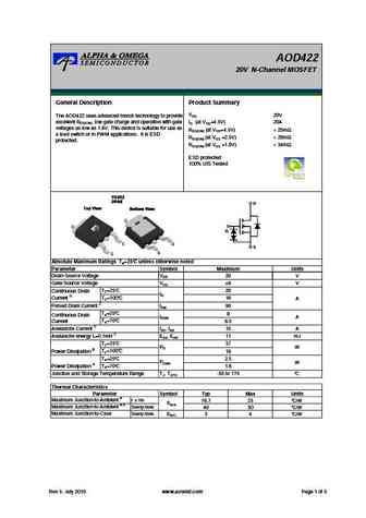
AOD422 20V N-Channel MOSFET General Description Product Summary VDS 20V The AOD422 uses advanced trench technology to provide excellent RDS(ON), low gate charge and operation with gate ID (at VGS=4.5V) 20A voltages as low as 1.8V. This device is suitable for use as RDS(ON) (at VGS=4.5V)
9.9. Size:846K cn vbsemi
aod425.pdf 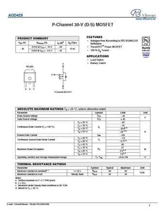
AOD425 www.VBsemi.tw P-Channel 30-V (D-S) MOSFET FEATURES PRODUCT SUMMARY Halogen-free According to IEC 61249-2-21 VDS (V) RDS(on) ( ) ID (A)d Qg (Typ.) Definition 0.018 at VGS = - 10 V - 40 TrenchFET Power MOSFET - 30 13 nC 100 % Rg Tested 0.025 at VGS = - 4.5 V - 35 APPLICATIONS Load Switch Battery Switch S TO-252 G D G D S P-Channel MOSFET ABSO
9.10. Size:895K cn vbsemi
aod422.pdf 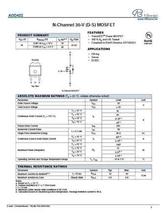
AOD422 www.VBsemi.tw N-Channel 30-V (D-S) MOSFET FEATURES PRODUCT SUMMARY TrenchFET Power MOSFET VDS (V) RDS(on) ( ) ID (A)a, e Qg (Typ) 100 % Rg and UIS Tested Compliant to RoHS Directive 2011/65/EU 0.007 at VGS = 10 V 50 30 25 nC 0.009 at VGS = 4.5 V 40 APPLICATIONS D OR-ing Server TO-252 DC/DC G G D S S Top View N-Channel MOSFET ABSOLUT
9.11. Size:223K inchange semiconductor
aod4286.pdf 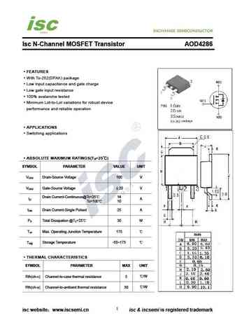
Isc N-Channel MOSFET Transistor AOD4286 FEATURES With To-252(DPAK) package Low input capacitance and gate charge Low gate input resistance 100% avalanche tested Minimum Lot-to-Lot variations for robust device performance and reliable operation APPLICATIONS Switching applications ABSOLUTE MAXIMUM RATINGS(T =25 ) a SYMBOL PARAMETER VALUE UNIT V Drain-Source Voltag
9.12. Size:265K inchange semiconductor
aod421.pdf 
isc P-Channel MOSFET Transistor AOD421 FEATURES Drain Current I = -12.5A@ T =25 D C Drain Source Voltage- V = -20V(Min) DSS Static Drain-Source On-Resistance R = 75m (Max) DS(on) 100% avalanche tested Minimum Lot-to-Lot variations for robust device performance and reliable operation DESCRIPTION Designed for use in switch mode power supplies and general purp
9.13. Size:207K inchange semiconductor
aod423.pdf 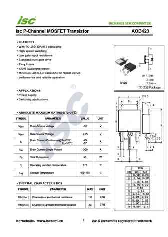
INCHANGE Semiconductor isc P-Channel MOSFET Transistor AOD423 FEATURES With TO-252( DPAK ) packaging High speed switching Low gate input resistance Standard level gate drive Easy to use 100% avalanche tested Minimum Lot-to-Lot variations for robust device performance and reliable operation APPLICATIONS Power supply Switching applications ABSOLUTE MAXIMUM RA
9.14. Size:264K inchange semiconductor
aod425.pdf 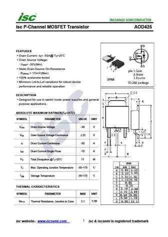
isc P-Channel MOSFET Transistor AOD425 FEATURES Drain Current I = -50A@ T =25 D C Drain Source Voltage- V = -30V(Min) DSS Static Drain-Source On-Resistance R = 17m (Max) DS(on) 100% avalanche tested Minimum Lot-to-Lot variations for robust device performance and reliable operation DESCRIPTION Designed for use in switch mode power supplies and general purpos
9.15. Size:265K inchange semiconductor
aod422.pdf 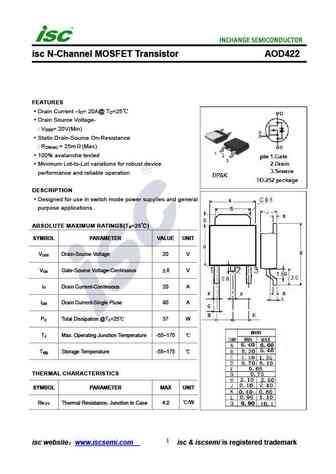
isc N-Channel MOSFET Transistor AOD422 FEATURES Drain Current I = 20A@ T =25 D C Drain Source Voltage- V = 20V(Min) DSS Static Drain-Source On-Resistance R = 25m (Max) DS(on) 100% avalanche tested Minimum Lot-to-Lot variations for robust device performance and reliable operation DESCRIPTION Designed for use in switch mode power supplies and general purpose
Другие MOSFET... AOC2870
, AOC2874
, AOC3860
, AOC3862
, AOC3864
, AOC3868
, AOC3870
, AOD409G
, 13N50
, AOD442G
, AOD522P
, AOD558
, AOD607A
, AOD661
, AOD294A
, AOD296A
, AOD2146
.
History: SMK0850F
| STD3PK50Z
| AO4292E
| 30N06G-TF3-T
| AO4268
| AGM405AP1
| 2SK3575-S
