AP1004CMX datasheet, аналоги, основные параметры
Наименование производителя: AP1004CMX 📄📄
Тип транзистора: MOSFET
Полярность: N
Предельные значения
Pd ⓘ - Максимальная рассеиваемая мощность: 2.8 W
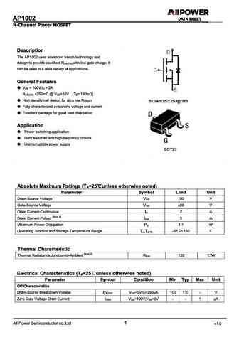
|Vds|ⓘ - Максимально допустимое напряжение сток-исток: 30 V
|Vgs|ⓘ - Максимально допустимое напряжение затвор-исток: 20 V
|Id| ⓘ - Максимально допустимый постоянный ток стока: 32 A
Tj ⓘ - Максимальная температура канала: 150 °C
Электрические характеристики
tr ⓘ - Время нарастания: 130 ns
Cossⓘ - Выходная емкость: 1600 pf
RDSonⓘ - Сопротивление сток-исток открытого транзистора: 0.0018 Ohm
Тип корпуса: CHIP
📄📄 Копировать
Аналог (замена) для AP1004CMX
- подборⓘ MOSFET транзистора по параметрам
AP1004CMX даташит
..1. Size:133K ape
ap1004cmx.pdf 
AP1004CMX Halogen-Free Product Advanced Power N-CHANNEL ENHANCEMENT MODE Electronics Corp. POWER MOSFET Ultra-low Forward Diode D BVDSS 30V Low Conductance Loss RDS(ON) 1.8m Low Profile (
9.1. Size:132K ape
ap1005bsq.pdf 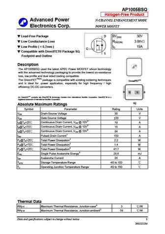
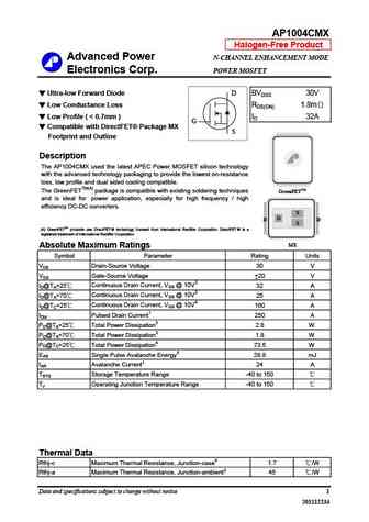
AP1005BSQ Halogen-Free Product Advanced Power N-CHANNEL ENHANCEMENT MODE Electronics Corp. POWER MOSFET Lead-Free Package D BVDSS 30V Low Conductance Loss RDS(ON) 3.8m Low Profile (
9.2. Size:104K ape
ap1001bsq.pdf 
AP1001BSQ Halogen-Free Product Advanced Power N-CHANNEL ENHANCEMENT MODE Electronics Corp. POWER MOSFET Lead-Free Package D BVDSS 30V Low Conductance Loss RDS(ON) 6m Low Profile (
9.3. Size:99K ape
ap1002bmx.pdf 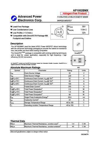
AP1002BMX Halogen-Free Product Advanced Power N-CHANNEL ENHANCEMENT MODE Electronics Corp. POWER MOSFET Lead-Free Package D BVDSS 30V Low Conductance Loss RDS(ON) 1.8m Low Profile (
9.4. Size:158K ape
ap1003bst.pdf 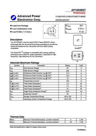
AP1003BST Preliminary Advanced Power N-CHANNEL ENHANCEMENT MODE Electronics Corp. POWER MOSFET Lead-Free Package D BVDSS 30V Low Conductance Loss RDS(ON) 4.7m Low Profile (
9.6. Size:1583K cn apm
ap100n03p ap100n03t.pdf 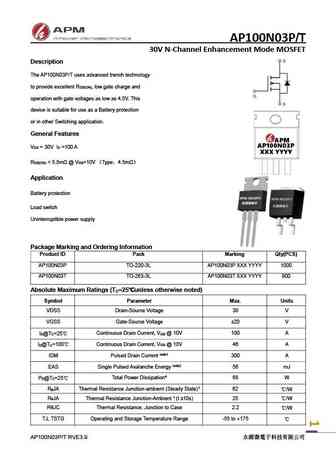
AP100N03P/T 30V N-Channel Enhancement Mode MOSFET Description The AP100N03P/T uses advanced trench technology to provide excellent R , low gate charge and DS(ON) operation with gate voltages as low as 4.5V. This device is suitable for use as a Battery protection or in other Switching application. General Features V = 30V I =100 A DS D R
9.7. Size:1377K cn apm
ap100n03ad.pdf 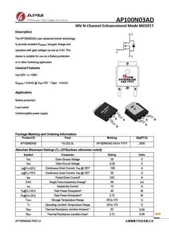
AP100N03AD 30V N-Channel Enhancement Mode MOSFET Description The AP100N03AD uses advanced trench technology to provide excellent R , low gate charge and DS(ON) operation with gate voltages as low as 4.5V. This device is suitable for use as a Battery protection or in other Switching application. General Features V =30V I =100A DS D R
9.8. Size:903K cn apm
ap100n04d.pdf 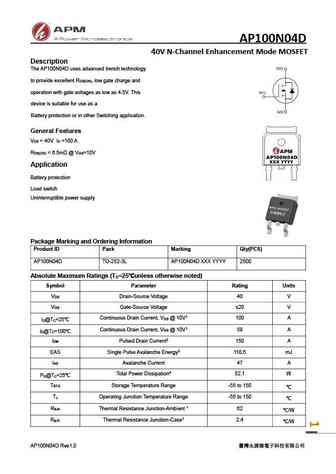
AP100N04D 40V N-Channel Enhancement Mode MOSFET Description The AP100N04D uses advanced trench technology to provide excellent R , low gate charge and DS(ON) operation with gate voltages as low as 4.5V. This device is suitable for use as a Battery protection or in other Switching application. General Features V = 40V I =100 A DS D R
9.9. Size:1461K cn apm
ap100n08d.pdf 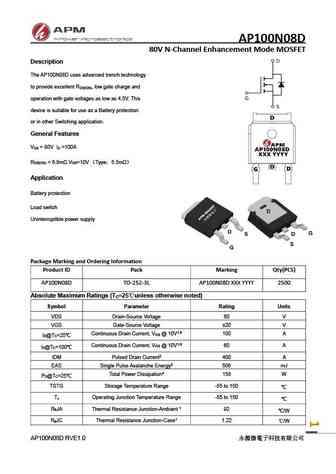
AP100N08D 80V N-Channel Enhancement Mode MOSFET Description The AP100N08D uses advanced trench technology to provide excellent R , low gate charge and DS(ON) operation with gate voltages as low as 4.5V. This device is suitable for use as a Battery protection or in other Switching application. General Features V = 80V I =100A DS D R
9.10. Size:1663K cn apm
ap100n03d.pdf 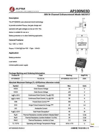
AP100N03D 30V N-Channel Enhancement Mode MOSFET Description The AP100N03D uses advanced trench technology to provide excellent R , low gate charge and DS(ON) operation with gate voltages as low as 4.5V. This device is suitable for use as a Battery protection or in other Switching application. General Features V = 30V I =100 A DS D R
9.11. Size:1322K cn apm
ap100n03y.pdf 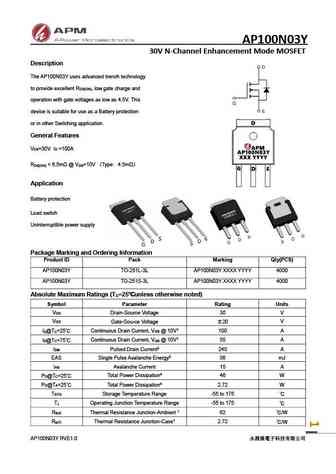
AP100N03Y 30V N-Channel Enhancement Mode MOSFET Description The AP100N03Y uses advanced trench technology to provide excellent R , low gate charge and DS(ON) operation with gate voltages as low as 4.5V. This device is suitable for use as a Battery protection or in other Switching application. General Features V =30V I =100A DS D R
9.12. Size:1150K cn apm
ap100p03d.pdf 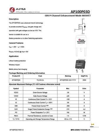
AP100P03D -30V P-Channel Enhancement Mode MOSFET Description The AP100P03D uses advanced trench technology to provide excellent R , low gate charge and DS(ON) operation with gate voltages as low as 4.5V. This device is suitable for use as a Battery protection or in other Switching application. General Features V = -30V I =-100A DS D R
9.13. Size:1239K cn apm
ap100p02nf.pdf 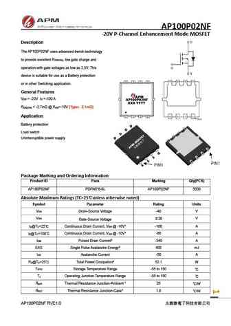
AP100P02NF -20V P-Channel Enhancement Mode MOSFET Description The AP100P02NF uses advanced trench technology to provide excellent R , low gate charge and DS(ON) operation with gate voltages as low as 2.5V. This device is suitable for use as a Battery protection or in other Switching application. General Features V = -20V I =-100 A DS D R
9.14. Size:1911K cn apm
ap100p04d.pdf 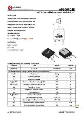
AP100P04D -40V P-Channel Enhancement Mode MOSFET Description The AP100P04D uses advanced trench technology to provide excellent R , low gate charge and DS(ON) operation with gate voltages as low as 4.5V. This device is suitable for use as a Battery protection or in other Switching application. General Features V = -40V I =-100 A DS D R
9.15. Size:1319K cn apm
ap100n04nf.pdf 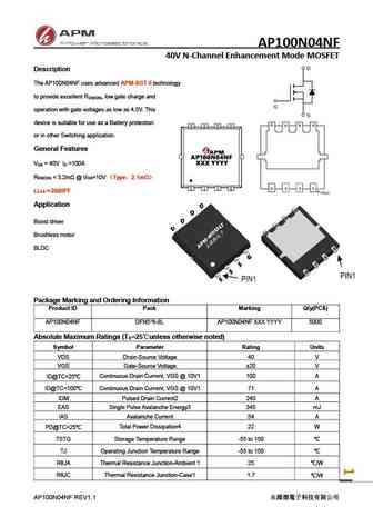
AP100N04NF 40V N-Channel Enhancement Mode MOSFET Description The AP100N04NF uses advanced APM-SGT II technology to provide excellent R , low gate charge and DS(ON) operation with gate voltages as low as 4.5V. This device is suitable for use as a Battery protection or in other Switching application. General Features V = 40V I =100A DS D R
Другие IGBT... AP05FN50I-HF, AP05N50I-HF, AP0803GMT-A-HF, AP0904GP-HF, AP09N20BGS-HF, AP09N70P-A-HF, AP09N70P-H-LF, AP1003BST, AON6380, AP1005BSQ, AP10N70I-A, AP10P10GK-HF, AP11N50I-HF, AP1203GH, AP1203GM, AP1333GU-HF, AP13N50W-HF