FDD6606 datasheet, аналоги, основные параметры
Наименование производителя: FDD6606 📄📄
Тип транзистора: MOSFET
Полярность: N
Предельные значения
Pd ⓘ - Максимальная рассеиваемая мощность: 71 W
|Vds|ⓘ - Максимально допустимое напряжение сток-исток: 30 V
|Vgs|ⓘ - Максимально допустимое напряжение затвор-исток: 20 V
|Id| ⓘ - Максимально допустимый постоянный ток стока: 75 A
Tj ⓘ - Максимальная температура канала: 175 °C
Электрические характеристики
tr ⓘ - Время нарастания: 12 ns
Cossⓘ - Выходная емкость: 577 pf
RDSonⓘ - Сопротивление сток-исток открытого транзистора: 0.006 Ohm
Тип корпуса: D-PAK
📄📄 Копировать
Аналог (замена) для FDD6606
- подборⓘ MOSFET транзистора по параметрам
FDD6606 даташит
fdd6606.pdf

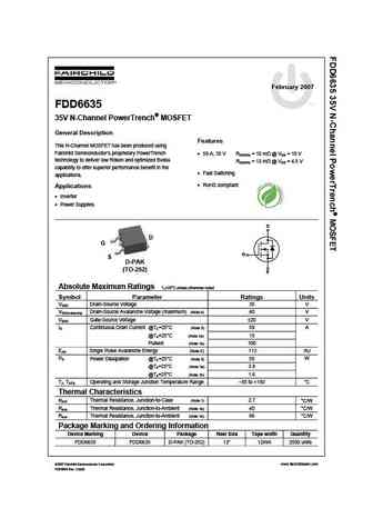
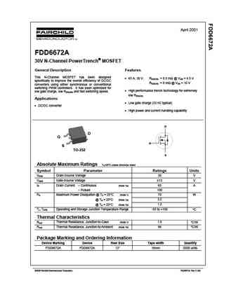
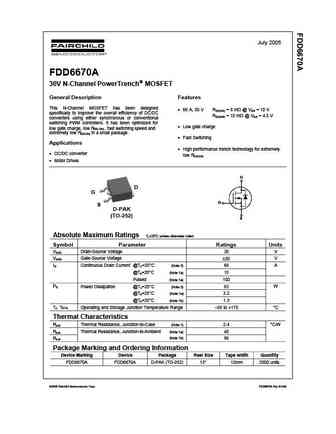
February 2004 FDD6606 30V N-Channel PowerTrench MOSFET General Description Features This N-Channel MOSFET has been designed 75 A, 30 V RDS(ON) = 6 m @ VGS = 10 V specifically to improve the overall efficiency of DC/DC RDS(ON) = 8 m @ VGS = 4.5 V converters using either synchronous or conventional switching PWM controllers. It has been optimized for Low gate
fdd6606.pdf

isc N-Channel MOSFET Transistor FDD6606 FEATURES Drain Current I =75A@ T =25 D C Drain Source Voltage V =20V(Min) DSS Static Drain-Source On-Resistance R =6m (Max) @ V = 10V DS(on) GS 100% avalanche tested Minimum Lot-to-Lot variations for robust device performance and reliable operation DESCRIPTION motor drive, DC-DC converter, power switch and solenoid dri
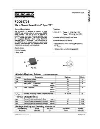
fdd6676s.pdf
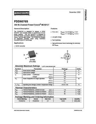
December 2002 FDD6676S 30V N-Channel PowerTrench MOSFET General Description Features The FDS6676S is designed to replace a DPAK 78 A, 30 V RDS(ON) = 6.0 m @ VGS = 10 V MOSFET and Schottky diode in synchronous DC DC RDS(ON) = 7.1 m @ VGS = 4.5 V power supplies. This 30V MOSFET is designed to maximize power conversion efficiency, providing a low Low gate charge
fdd6685.pdf
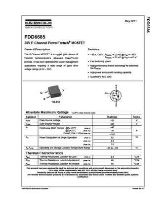
May 2011 FDD6685 30V P-Channel PowerTrench MOSFET General Description Features This P-Channel MOSFET is a rugged gate version of 40 A, 30 V. RDS(ON) = 20 m @ VGS = 10 V RDS(ON) = 30 m @ VGS = 4.5 V Fairchild Semiconductor s advanced PowerTrench Fast switching speed process. It has been optimized for power management applications requiring a wide
fdd6612a fdu6612a.pdf
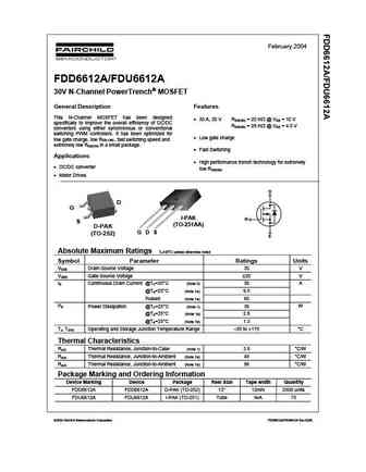
February 2004 FDD6612A/FDU6612A 30V N-Channel PowerTrench MOSFET General Description Features This N-Channel MOSFET has been designed 30 A, 30 V RDS(ON) = 20 m @ VGS = 10 V specifically to improve the overall efficiency of DC/DC RDS(ON) = 28 m @ VGS = 4.5 V converters using either synchronous or conventional switching PWM controllers. It has been optimized for Low gate
fdd6690a.pdf
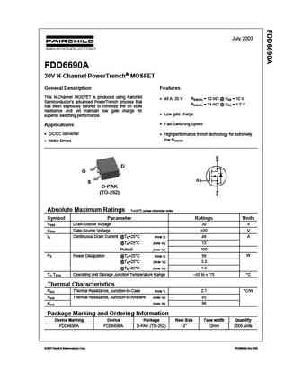
July 2003 FDD6690A 30V N-Channel PowerTrench MOSFET General Description Features This N-Channel MOSFET is produced using Fairchild 46 A, 30 V RDS(ON) = 12 m @ VGS = 10 V Semiconductor s advanced PowerTrench process that RDS(ON) = 14 m @ VGS = 4.5 V has been especially tailored to minimize the on state resistance and yet maintain low gate charge for Low gate charge su
fdd6670s.pdf
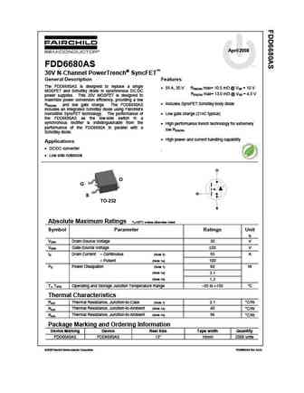
September 2001 FDD6670S 30V N-Channel PowerTrench SyncFET General Description Features The FDD6670S is designed to replace a single 64 A, 30 V RDS(ON) = 9 m @ VGS = 10 V MOSFET and Schottky diode in synchronous DC DC RDS(ON) = 12.5 m @ VGS = 4.5 V power supplies. This 30V MOSFET is designed to maximize power conversion efficiency, providing a low Includes S
fdd6630a.pdf
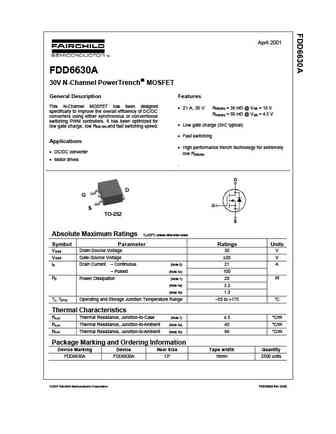
April 2001 FDD6630A 30V N-Channel PowerTrench MOSFET General Description Features This N-Channel MOSFET has been designed 21 A, 30 V R = 35 m @ V = 10 V DS(ON) GS specifically to improve the overall efficiency of DC/DC R = 50 m @ V = 4.5 V DS(ON) GS converters using either synchronous or conventional switching PWM controllers. It has been optimized for Low g
fdd6670al.pdf

May 2004 FDD6670AL 30V N-Channel PowerTrench MOSFET General Description Features This N-Channel MOSFET has been designed 84 A, 30 V. RDS(ON) = 5 m @ VGS = 10 V specifically to improve the overall efficiency of DC/DC RDS(ON) = 6 m @ VGS = 4.5 V converters using either synchronous or conventional switching PWM controllers. It has been optimized for Low gate c
fdd6676.pdf
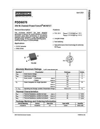
April 2001 FDD6676 30V N-Channel PowerTrench MOSFET General Description Features This N-Channel MOSFET has been designed 78 A, 30 V RDS(ON) = 7.5 m @ VGS = 10 V specifically to improve the overall efficiency of DC/DC RDS(ON) = 8.5 m @ VGS = 4.5 V converters using either synchronous or conventional switching PWM controllers. It has been optimized for
fdd6670as.pdf

May 2005 FDD6670AS 30V N-Channel PowerTrench SyncFET General Description Features The FDD6670AS is designed to replace a single 76 A, 30 V RDS(ON) max= 8.0 m @ VGS = 10 V MOSFET and Schottky diode in synchronous DC DC RDS(ON) max= 10.4 m @ VGS = 4.5 V power supplies. This 30V MOSFET is designed to maximize power conversion efficiency, providing a low Inclu
fdd6672a.pdf
April 2001 FDD6672A 30V N-Channel PowerTrench MOSFET General Description Features This N-Channel MOSFET has been designed 65 A, 30 V. RDS(ON) = 9.5 m @ VGS = 4.5 V specifically to improve the overall efficiency of DC/DC RDS(ON) = 8 m @ VGS = 10 V converters using either synchronous or conventional switching PWM controllers. It has been optimized for
fdd6644 fdu6644.pdf

April 2001 FDD6644/FDU6644 30V N-Channel PowerTrench MOSFET General Description Features This N-Channel MOSFET has been designed 67 A, 30 V. RDS(ON) = 8.5 m @ VGS = 10 V specifically to improve the overall efficiency of DC/DC RDS(ON) = 10.5 m @ VGS = 4.5 V converters using either synchronous or conventional switching PWM controllers. It has been opt
fdd6696.pdf
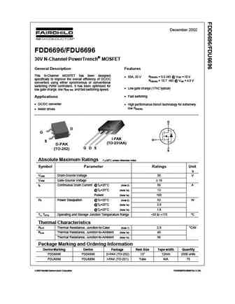
December 2002 FDD6696/FDU6696 30V N-Channel PowerTrench MOSFET General Description Features This N-Channel MOSFET has been designed 50A, 30 V R = 8.0 m @ V = 10 V DS(ON) GS specifically to improve the overall efficiency of DC/DC R = 10.7 m @ V = 4.5 V DS(ON) GS converters using either synchronous or conventional switching PWM controllers. It has been optimized for Low
fdd6680.pdf
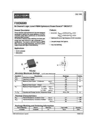
July 1999 FDD6680 N-Channel Logic Level PWM Optimized PowerTrench MOSFET Features General Description This N-Channel Logic level MOSFET has been designed 55 A, 30 V. RDS(on) = 0.010 @ VGS = 10 V specifically to improve the overall efficiency of DC/DC RDS(on) = 0.015 @ VGS = 4.5 V. converters using either synchronous or conventional switching PWM controllers. Optimi
fdd6637 f085.pdf
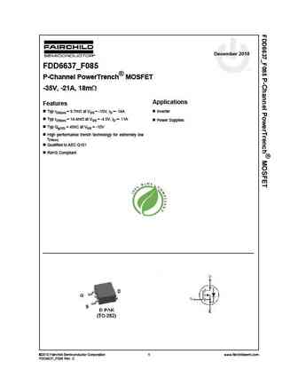
December 2010 FDD6637_F085 P-Channel PowerTrench MOSFET -35V, -21A, 18m Applications Features Typ rDS(on) = 9.7m at VGS = -10V, ID =- 14A Inverter Typ rDS(on) = 14.4m at VGS = -4.5V, ID =- 11A Power Supplies Typ Qg(10) = 45nC at VGS = -10V High performance trench technology for extremely low rDS(on). Qualified to AEC Q101 RoHS Compliant 2010 Fairchild Sem
fdd6692 fdu6692.pdf

April 2001 FDD6692/FDU6692 30V N-Channel PowerTrench MOSFET General Description Features This N-Channel MOSFET has been designed 54 A, 30 V. RDS(ON) = 12 m @ VGS = 10 V specifically to improve the overall efficiency of DC/DC RDS(ON) = 14.5 m @ VGS = 4.5 V converters using either synchronous or conventional switching PWM controllers. It has been optim
fdd6670a.pdf
July 2005 FDD6670A 30V N-Channel PowerTrench MOSFET General Description Features This N-Channel MOSFET has been designed 66 A, 30 V RDS(ON) = 8 m @ VGS = 10 V specifically to improve the overall efficiency of DC/DC RDS(ON) = 10 m @ VGS = 4.5 V converters using either synchronous or conventional switching PWM controllers. It has been optimized for Low gate charge low ga
fdd6680as.pdf
April 2008 FDD6680AS tm 30V N-Channel PowerTrench SyncFET General Description Features The FDD6680AS is designed to replace a single 55 A, 30 V RDS(ON) max= 10.5 m @ VGS = 10 V MOSFET and Schottky diode in synchronous DC DC RDS(ON) max= 13.0 m @ VGS = 4.5 V power supplies. This 30V MOSFET is designed to maximize power conversion efficiency, providing a low
fdd6632.pdf
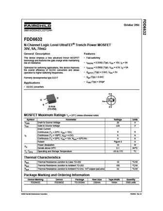
October 2004 FDD6632 N-Channel Logic Level UltraFET Trench Power MOSFET 30V, 9A, 70m General Description Features This device employs a new advanced trench MOSFET Fast switching technology and features low gate charge while maintaining rDS(ON) = 0.058 (Typ), VGS = 10V, ID = 9A low on-resistance. rDS(ON) = 0.090 (Typ), VGS = 4.5V, ID = 6A Optimized for switching
fdd6680s.pdf
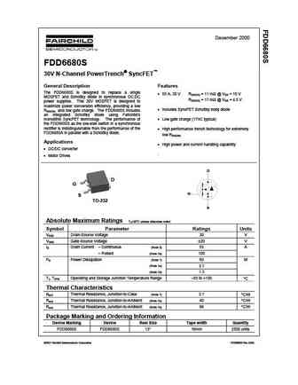
December 2000 FDD6680S 30V N-Channel PowerTrench SyncFET General Description Features The FDD6680S is designed to replace a single 55 A, 30 V RDS(ON) = 11 m @ VGS = 10 V MOSFET and Schottky diode in synchronous DC DC RDS(ON) = 17 m @ VGS = 4.5 V power supplies. This 30V MOSFET is designed to maximize power conversion efficiency, providing a low Inclu
fdd6682 dss20201l.pdf

June 2004 FDD6682/FDU6682 30V N-Channel PowerTrench MOSFET General Description Features This N-Channel MOSFET has been designed 75 A, 30 V RDS(ON) = 6.2 m @ VGS = 10 V specifically to improve the overall efficiency of DC/DC RDS(ON) = 8.0 m @ VGS = 4.5 V converters using either synchronous or conventional switching PWM controllers. It has been optimized for Low gate charg
fdd6688s.pdf
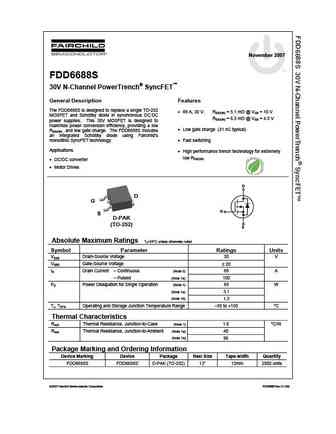
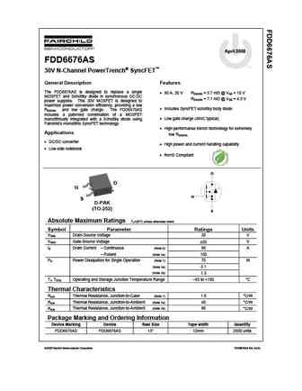
November 2007 tm FDD6688S 30V N-Channel PowerTrench SyncFET General Description Features The FDD6688S is designed to replace a single TO-252 88 A, 30 V. RDS(ON) = 5.1 m @ VGS = 10 V MOSFET and Schottky diode in synchronous DC DC RDS(ON) = 6.3 m @ VGS = 4.5 V power supplies. This 30V MOSFET is designed to maximize power conversion efficiency, providing a low
fdd6682.pdf

June 2004 FDD6682/FDU6682 30V N-Channel PowerTrench MOSFET General Description Features This N-Channel MOSFET has been designed 75 A, 30 V RDS(ON) = 6.2 m @ VGS = 10 V specifically to improve the overall efficiency of DC/DC RDS(ON) = 8.0 m @ VGS = 4.5 V converters using either synchronous or conventional switching PWM controllers. It has been optimized for Low gate charg
fdd6688 fdd6688 fdu6688.pdf

June 2004 FDD6688/FDU6688 30V N-Channel PowerTrench MOSFET General Description Features This N-Channel MOSFET has been designed 84 A, 30 V. RDS(ON) = 5 m @ VGS = 10 V specifically to improve the overall efficiency of DC/DC RDS(ON) = 6 m @ VGS = 4.5 V converters using either synchronous or conventional switching PWM controllers. It has been optimized for Low gate charge
fdd6637.pdf
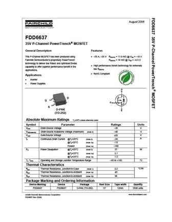
August 2006 FDD6637 35V P-Channel PowerTrench MOSFET General Description Features This P-Channel MOSFET has been produced using 55 A, 35 V RDS(ON) = 11.6 m @ VGS = 10 V Fairchild Semiconductor s proprietary PowerTrench RDS(ON) = 18 m @ VGS = 4.5 V technology to deliver low Rdson and optimized Bvdss High performance trench technology for extremely capa
fdd6680a.pdf
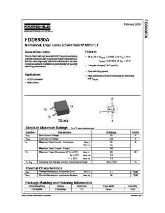
February 2000 FDD6680A N-Channel, Logic Level, PowerTrench MOSFET Features General Description This N-Channel Logic level MOSFET is produced using 56 A, 30 V. RDS(ON) = 0.0095 @ VGS = 10 V Fairchild Semiconductor's advanced PowerTrench process RDS(ON) = 0.0130 @ VGS = 4.5 V. that has been especially tailored to minimize the on-state resistance and y
fdd6676as.pdf
April 2008 FDD6676AS tm 30V N-Channel PowerTrench SyncFET General Description Features The FDD6676AS is designed to replace a single 90 A, 30 V RDS(ON) = 5.7 m @ VGS = 10 V MOSFET and Schottky diode in synchronous DC DC RDS(ON) = 7.1 m @ VGS = 4.5 V power supplies. This 30V MOSFET is designed to maximize power conversion efficiency, providing a low Includ
fdd6685.pdf

February 2004 FDD6685 30V P-Channel PowerTrench MOSFET General Description Features This P-Channel MOSFET is a rugged gate version of 40 A, 30 V. RDS(ON) = 20 m @ VGS = 10 V RDS(ON) = 30 m @ VGS = 4.5 V Fairchild Semiconductor s advanced PowerTrench Fast switching speed process. It has been optimized for power management applications requiring a
fdd6612a fdu6612a.pdf

February 2004 FDD6612A/FDU6612A 30V N-Channel PowerTrench MOSFET General Description Features This N-Channel MOSFET has been designed 30 A, 30 V RDS(ON) = 20 m @ VGS = 10 V specifically to improve the overall efficiency of DC/DC RDS(ON) = 28 m @ VGS = 4.5 V converters using either synchronous or conventional switching PWM controllers. It has been optimized for Low gate
fdd6630a.pdf
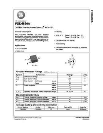
FDD6630A 30V N-Channel PowerTrench MOSFET General Description Features This N-Channel MOSFET has been designed 21 A, 30 V R = 35 m @ V = 10 V DS(ON) GS specifically to improve the overall efficiency of DC/DC R = 50 m @ V = 4.5 V DS(ON) GS converters using either synchronous or conventional switching PWM controllers. It has been optimized for Low gate charge (5n
fdd6637.pdf

Is Now Part of To learn more about ON Semiconductor, please visit our website at www.onsemi.com Please note As part of the Fairchild Semiconductor integration, some of the Fairchild orderable part numbers will need to change in order to meet ON Semiconductor s system requirements. Since the ON Semiconductor product management systems do not have the ability to manage part nomenclatur
fdd6685.pdf
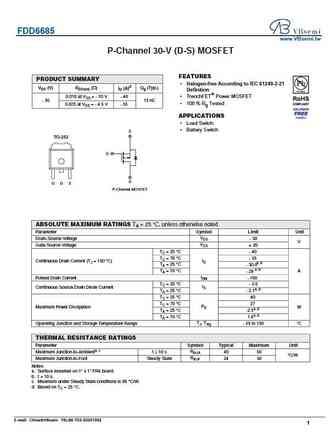
FDD6685 www.VBsemi.tw P-Channel 30-V (D-S) MOSFET FEATURES PRODUCT SUMMARY Halogen-free According to IEC 61249-2-21 VDS (V) RDS(on) ( ) ID (A)d Qg (Typ.) Definition 0.018 at VGS = - 10 V - 40 TrenchFET Power MOSFET - 30 13 nC 100 % Rg Tested 0.025 at VGS = - 4.5 V - 35 APPLICATIONS Load Switch Battery Switch S TO-252 G D G D S P-Channel MOSFET ABS
fdd6680.pdf
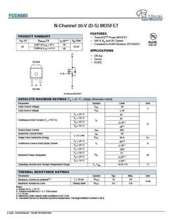
FDD6680 www.VBsemi.tw N-Channel 30-V (D-S) MOSFET FEATURES PRODUCT SUMMARY TrenchFET Power MOSFET VDS (V) RDS(on) ( ) ID (A)a, e Qg (Typ) 100 % Rg and UIS Tested Compliant to RoHS Directive 2011/65/EU 0.007 at VGS = 10 V 50 30 25 nC 0.009 at VGS = 4.5 V 40 APPLICATIONS D OR-ing Server TO-252 DC/DC G G D S S Top View N-Channel MOSFET ABSOLU
fdd6637.pdf

FDD6637 www.VBsemi.tw P-Channel 30 V (D-S) MOSFET FEATURES PRODUCT SUMMARY Compliant to RoHS Directive 2002/95/EC VDS (V) RDS(on) ( )ID (A)a Available 0.009 at VGS = - 10 V 80 RoHS* - 30 COMPLIANT 0.012 at VGS = - 4.5 V 80 S TO-252 G D G S D Top View P-Channel MOSFET ABSOLUTE MAXIMUM RATINGS (TC = 25 C, unless otherwise noted) Parameter Symbol Limit Unit Ga
fdd6635.pdf

isc N-Channel MOSFET Transistor FDD6635 FEATURES Drain Current I =59A@ T =25 D C Drain Source Voltage V =35V(Min) DSS Static Drain-Source On-Resistance R =10m (Max) @ V = 10V DS(on) GS 100% avalanche tested Minimum Lot-to-Lot variations for robust device performance and reliable operation DESCRIPTION motor drive, DC-DC converter, power switch and solenoid dr
fdd6676s.pdf
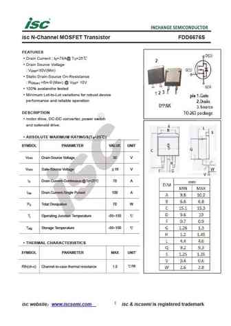
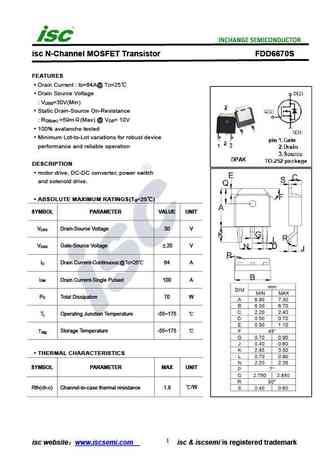
isc N-Channel MOSFET Transistor FDD6676S FEATURES Drain Current I =78A@ T =25 D C Drain Source Voltage V =30V(Min) DSS Static Drain-Source On-Resistance R =6m (Max) @ V = 10V DS(on) GS 100% avalanche tested Minimum Lot-to-Lot variations for robust device performance and reliable operation DESCRIPTION motor drive, DC-DC converter, power switch and solenoid dr
fdd6692.pdf

isc N-Channel MOSFET Transistor FDD6692 FEATURES Drain Current I =54A@ T =25 D C Drain Source Voltage V =30V(Min) DSS Static Drain-Source On-Resistance R =12m (Max) @ V = 10V DS(on) GS 100% avalanche tested Minimum Lot-to-Lot variations for robust device performance and reliable operation DESCRIPTION motor drive, DC-DC converter, power switch and solenoid dr
fdd6690a.pdf

isc N-Channel MOSFET Transistor FDD6690A FEATURES Drain Current I =46A@ T =25 D C Drain Source Voltage V =30V(Min) DSS Static Drain-Source On-Resistance R =12m (Max) @ V = 10V DS(on) GS 100% avalanche tested Minimum Lot-to-Lot variations for robust device performance and reliable operation DESCRIPTION motor drive, DC-DC converter, power switch and solenoid d
fdd6670s.pdf
isc N-Channel MOSFET Transistor FDD6670S FEATURES Drain Current I =64A@ T =25 D C Drain Source Voltage V =30V(Min) DSS Static Drain-Source On-Resistance R =59m (Max) @ V = 10V DS(on) GS 100% avalanche tested Minimum Lot-to-Lot variations for robust device performance and reliable operation DESCRIPTION motor drive, DC-DC converter, power switch and solenoid d
fdd6670al.pdf

isc N-Channel MOSFET Transistor FDD6670AL FEATURES Drain Current I =84A@ T =25 D C Drain Source Voltage V =30V(Min) DSS Static Drain-Source On-Resistance R =5m (Max) @ V = 10V DS(on) GS 100% avalanche tested Minimum Lot-to-Lot variations for robust device performance and reliable operation DESCRIPTION motor drive, DC-DC converter, power switch and solenoid d
fdd6676.pdf

isc N-Channel MOSFET Transistor FDD6676 FEATURES Drain Current I =78A@ T =25 D C Drain Source Voltage V =30V(Min) DSS Static Drain-Source On-Resistance R =7.5m (Max) @ V = 10V DS(on) GS 100% avalanche tested Minimum Lot-to-Lot variations for robust device performance and reliable operation DESCRIPTION motor drive, DC-DC converter, power switch and solenoid d
fdd6644.pdf

isc N-Channel MOSFET Transistor FDD6644 FEATURES Drain Current I =67A@ T =25 D C Drain Source Voltage V =30V(Min) DSS Static Drain-Source On-Resistance R =8.5m (Max) @ V = 10V DS(on) GS 100% avalanche tested Minimum Lot-to-Lot variations for robust device performance and reliable operation DESCRIPTION motor drive, DC-DC converter, power switch and solenoid d
fdd6672a.pdf

isc N-Channel MOSFET Transistor FDD6672A FEATURES Drain Current I =65A@ T =25 D C Drain Source Voltage V =30V(Min) DSS Static Drain-Source On-Resistance R =8m (Max) @ V = 10V DS(on) GS 100% avalanche tested Minimum Lot-to-Lot variations for robust device performance and reliable operation DESCRIPTION motor drive, DC-DC converter, power switch and solenoid dr
fdd6696.pdf

isc N-Channel MOSFET Transistor FDD6696 FEATURES Drain Current I =50A@ T =25 D C Drain Source Voltage V =30V(Min) DSS Static Drain-Source On-Resistance R =8m (Max) @ V = 10V DS(on) GS 100% avalanche tested Minimum Lot-to-Lot variations for robust device performance and reliable operation DESCRIPTION motor drive, DC-DC converter, power switch and solenoid dri
fdd6680.pdf

isc N-Channel MOSFET Transistor FDD6680 FEATURES Drain Current I =46A@ T =25 D C Drain Source Voltage V =30V(Min) DSS Static Drain-Source On-Resistance R =10m (Max) @ V = 10V DS(on) GS 100% avalanche tested Minimum Lot-to-Lot variations for robust device performance and reliable operation DESCRIPTION motor drive, DC-DC converter, power switch and solenoid dr
fdd6670a.pdf

isc N-Channel MOSFET Transistor FDD6670A FEATURES Drain Current I =66A@ T =25 D C Drain Source Voltage V =30V(Min) DSS Static Drain-Source On-Resistance R =8m (Max) @ V = 10V DS(on) GS 100% avalanche tested Minimum Lot-to-Lot variations for robust device performance and reliable operation DESCRIPTION motor drive, DC-DC converter, power switch and solenoid dr
fdd6680as.pdf
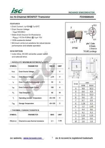
isc N-Channel MOSFET Transistor FDD6680AS FEATURES Drain Current I =55A@ T =25 D C Drain Source Voltage V =30V(Min) DSS Static Drain-Source On-Resistance R =10.5m (Max) @ V = 10V DS(on) GS 100% avalanche tested Minimum Lot-to-Lot variations for robust device performance and reliable operation DESCRIPTION motor drive, DC-DC converter, power switch and solenoi
fdd6632.pdf
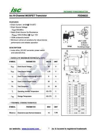
isc N-Channel MOSFET Transistor FDD6632 FEATURES Drain Current I =9A@ T =25 D C Drain Source Voltage V =20V(Min) DSS Static Drain-Source On-Resistance R =90m (Max) @ V = 10V DS(on) GS 100% avalanche tested Minimum Lot-to-Lot variations for robust device performance and reliable operation DESCRIPTION motor drive, DC-DC converter, power switch and solenoid dri
fdd6680s.pdf

isc N-Channel MOSFET Transistor FDD6680S FEATURES Drain Current I =55A@ T =25 D C Drain Source Voltage V =30V(Min) DSS Static Drain-Source On-Resistance R =11m (Max) @ V = 10V DS(on) GS 100% avalanche tested Minimum Lot-to-Lot variations for robust device performance and reliable operation DESCRIPTION motor drive, DC-DC converter, power switch and solenoid d
fdd6688.pdf

isc N-Channel MOSFET Transistor FDD6688 FEATURES Drain Current I =84A@ T =25 D C Drain Source Voltage V =30V(Min) DSS Static Drain-Source On-Resistance R =5m (Max) @ V = 10V DS(on) GS 100% avalanche tested Minimum Lot-to-Lot variations for robust device performance and reliable operation DESCRIPTION motor drive, DC-DC converter, power switch and solenoid dri
fdd6688s.pdf

isc N-Channel MOSFET Transistor FDD6688S FEATURES Drain Current I =88A@ T =25 D C Drain Source Voltage V =30V(Min) DSS Static Drain-Source On-Resistance R =5.1m (Max) @ V = 10V DS(on) GS 100% avalanche tested Minimum Lot-to-Lot variations for robust device performance and reliable operation DESCRIPTION motor drive, DC-DC converter, power switch and solenoid
fdd6682.pdf

isc N-Channel MOSFET Transistor FDD6682 FEATURES Drain Current I =75A@ T =25 D C Drain Source Voltage V =30V(Min) DSS Static Drain-Source On-Resistance R =6.2m (Max) @ V = 10V DS(on) GS 100% avalanche tested Minimum Lot-to-Lot variations for robust device performance and reliable operation DESCRIPTION motor drive, DC-DC converter, power switch and solenoid d
fdd6680a.pdf

isc N-Channel MOSFET Transistor FDD6680A FEATURES Drain Current I =56A@ T =25 D C Drain Source Voltage V =30V(Min) DSS Static Drain-Source On-Resistance R =9.5m (Max) @ V = 10V DS(on) GS 100% avalanche tested Minimum Lot-to-Lot variations for robust device performance and reliable operation DESCRIPTION motor drive, DC-DC converter, power switch and solenoid
Другие IGBT... FDD26AN06A0, FDD3570, FDD3N50NZTM, FDD45AN06LA0, FDD45AN06LA0F085, FDD5810, FDD5N60NZTM, FDD6512A, IRLZ44N, FDD6632, FDD6670AL, FDD6670AS, FDD6672A, FDD6676AS, FDD6682, FDD6688S, FDD6696
Параметры MOSFET. Взаимосвязь и компромиссы
🌐 : EN ES РУ

Список транзисторов
Обновления
MOSFET: CEZC2P07 | CEZ2R05 | CEU3133 | CES2361 | CES2312A | CEP100N10L | CEM3425 | CEM3139 | CEM3133 | CEM3115 | CED3133 | CEC3257 | CEC2533 | CEB100N10L | BC3134KT | BC3134K
Popular searches
irf3205 datasheet | irf5210 | mj15024 | 2n2219 | tip42c | 2sc2240 | bc547 transistor equivalent | 2sa1943