MTP30N08M. Аналоги и основные параметры
Наименование производителя: MTP30N08M
Тип транзистора: MOSFET
Полярность: N
Предельные значения
Pd ⓘ
- Максимальная рассеиваемая мощность: 125 W
|Vds|ⓘ - Максимально допустимое напряжение сток-исток: 80 V
|Vgs|ⓘ - Максимально допустимое напряжение затвор-исток: 20 V
|Id| ⓘ - Максимально допустимый постоянный ток стока: 30 A
Tj ⓘ - Максимальная температура канала: 150 °C
Электрические характеристики
Cossⓘ - Выходная емкость: 1800 pf
RDSonⓘ - Сопротивление сток-исток открытого транзистора: 0.065 Ohm
Тип корпуса: TO220
Аналог (замена) для MTP30N08M
- подборⓘ MOSFET транзистора по параметрам
MTP30N08M даташит
7.2. Size:207K motorola
mtp30n06vl.pdf 
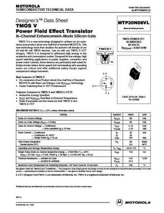
MOTOROLA Order this document SEMICONDUCTOR TECHNICAL DATA by MTP30N06VL/D Designer's Data Sheet MTP30N06VL TMOS V Motorola Preferred Device Power Field Effect Transistor N Channel Enhancement Mode Silicon Gate TMOS POWER FET TMOS V is a new technology designed to achieve an on resis- 30 AMPERES tance area product about one half that of standard MOSFETs. This 60 VOLTS
9.1. Size:191K motorola
mtp30p06v .pdf 
MOTOROLA Order this document SEMICONDUCTOR TECHNICAL DATA by MTP30P06V/D Designer's Data Sheet MTP30P06V TMOS V Motorola Preferred Device Power Field Effect Transistor P Channel Enhancement Mode Silicon Gate TMOS POWER FET TMOS V is a new technology designed to achieve an on resis- 30 AMPERES tance area product about one half that of standard MOSFETs. This 60 VOLTS new
9.2. Size:161K motorola
mtp3055vlrev2a.pdf 
MOTOROLA Order this document SEMICONDUCTOR TECHNICAL DATA by MTP3055VL/D Designer's Data Sheet MTP3055VL TMOS V Motorola Preferred Device Power Field Effect Transistor N Channel Enhancement Mode Silicon Gate TMOS POWER FET TMOS V is a new technology designed to achieve an on resis- 12 AMPERES tance area product about one half that of standard MOSFETs. This 60 VOLTS
9.3. Size:144K motorola
mtp3055vl.pdf 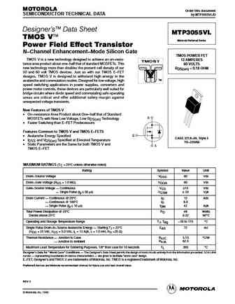
MOTOROLA Order this document SEMICONDUCTOR TECHNICAL DATA by MTP3055VL/D Designer's Data Sheet MTP3055VL TMOS V Motorola Preferred Device Power Field Effect Transistor N Channel Enhancement Mode Silicon Gate TMOS POWER FET TMOS V is a new technology designed to achieve an on resis- 12 AMPERES tance area product about one half that of standard MOSFETs. This 60 VOLTS
9.4. Size:160K motorola
mtp3055vrev2a.pdf 
MOTOROLA Order this document SEMICONDUCTOR TECHNICAL DATA by MTP3055V/D Designer's Data Sheet MTP3055V TMOS V Motorola Preferred Device Power Field Effect Transistor N Channel Enhancement Mode Silicon Gate TMOS POWER FET TMOS V is a new technology designed to achieve an on resis- 12 AMPERES tance area product about one half that of standard MOSFETs. This 60 VOLTS
9.5. Size:142K motorola
mtp3055v.pdf 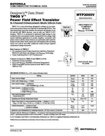
MOTOROLA Order this document SEMICONDUCTOR TECHNICAL DATA by MTP3055V/D Designer's Data Sheet MTP3055V TMOS V Motorola Preferred Device Power Field Effect Transistor N Channel Enhancement Mode Silicon Gate TMOS POWER FET TMOS V is a new technology designed to achieve an on resis- 12 AMPERES tance area product about one half that of standard MOSFETs. This 60 VOLTS
9.6. Size:166K motorola
mtp30p06v.pdf 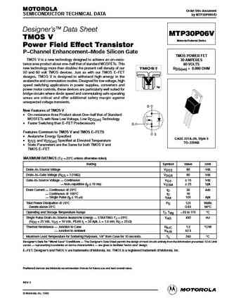
MOTOROLA Order this document SEMICONDUCTOR TECHNICAL DATA by MTP30P06V/D Designer's Data Sheet MTP30P06V TMOS V Motorola Preferred Device Power Field Effect Transistor P Channel Enhancement Mode Silicon Gate TMOS POWER FET TMOS V is a new technology designed to achieve an on resis- 30 AMPERES tance area product about one half that of standard MOSFETs. This 60 VOLTS new
9.8. Size:294K st
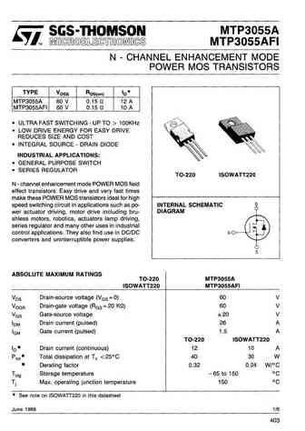
mtp3055e.pdf 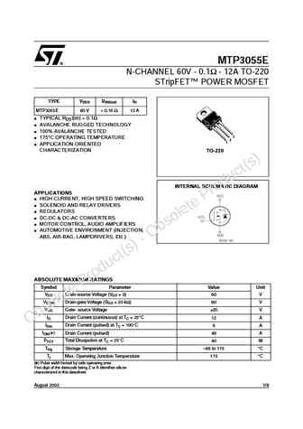
MTP3055E N-CHANNEL 60V - 0.1 - 12ATO-220 STripFET POWER MOSFET TYPE VDSS RDS(on) ID MTP3055E 60 V
9.9. Size:42K fairchild semi
mtp3055vl.pdf 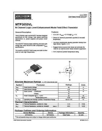
June 2000 DISTRIBUTION GROUP* MTP3055VL N-Channel Logic Level Enhancement Mode Field Effect Transistor Features General Description 12 A, 60 V. RDS(ON) = 0.18 @ VGS = 5 V This N-Channel Logic Level MOSFET has been designed specifically for low voltage, high speed switching Critical DC electrical parameters specified at elevated applications i.e. power supplies and power mo
9.10. Size:202K onsemi
mtp3055v.pdf 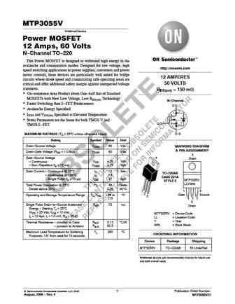
MTP3055V Preferred Device Power MOSFET 12 Amps, 60 Volts N-Channel TO-220 This Power MOSFET is designed to withstand high energy in the avalanche and commutation modes. Designed for low voltage, high http //onsemi.com speed switching applications in power supplies, converters and power motor controls, these devices are particularly well suited for bridge 12 AMPERES circuits where dio
9.11. Size:204K onsemi
mtp30p06v.pdf 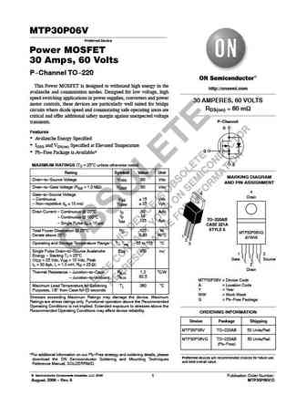
MTP30P06V Preferred Device Power MOSFET 30 Amps, 60 Volts P-Channel TO-220 This Power MOSFET is designed to withstand high energy in the http //onsemi.com avalanche and commutation modes. Designed for low voltage, high speed switching applications in power supplies, converters and power 30 AMPERES, 60 VOLTS motor controls, these devices are particularly well suited for bridge RDS(on)
9.12. Size:221K cystek
mtp3001n3.pdf 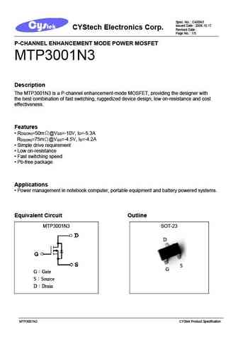
Spec. No. C400N3 Issued Date 2006.10.17 CYStech Electronics Corp. Revised Date Page No. 1/5 P-CHANNEL ENHANCEMENT MODE POWER MOSFET MTP3001N3 Description The MTP3001N3 is a P-channel enhancement-mode MOSFET, providing the designer with the best combination of fast switching, ruggedized device design, low on-resistance and cost effectiveness. Features @V =-10V,
9.13. Size:478K jiejie micro
jmtp3008a.pdf 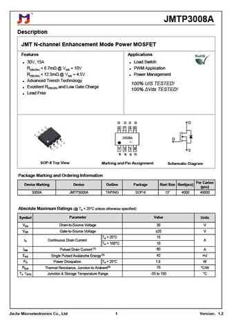
JMTP3008A Description JMT N-channel Enhancement Mode Power MOSFET Features Applications 30V, 15A Load Switch RDS(ON)
9.14. Size:400K jiejie micro
jmtp3010d.pdf 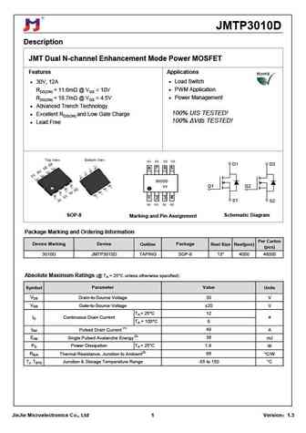
JMTP3010D Description JMT Dual N-channel Enhancement Mode Power MOSFET Features Applications 30V, 12A Load Switch RDS(ON)
Другие MOSFET... MNT-LB32N20-C4
, MTB30N06VL
, MTB30P06V
, MTB35N06ZL
, MTP10N10M
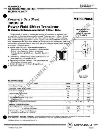
, MTP3055E
, MTP3055EFI
, MTP30N05E
, IRF2807
, MTP3N50E
, MTP3N60
, MTP3N60FI
, MTP6N60
, NDB4050
, NDB4050L
, NDB4060
, NDB4060L
.