NDT456P datasheet, аналоги, основные параметры
Наименование производителя: NDT456P 📄📄
Тип транзистора: MOSFET
Полярность: P
Предельные значения
Pd ⓘ - Максимальная рассеиваемая мощность: 3 W
|Vds|ⓘ - Максимально допустимое напряжение сток-исток: 30 V
|Vgs|ⓘ - Максимально допустимое напряжение затвор-исток: 20 V
|Id| ⓘ - Максимально допустимый постоянный ток стока: 7.5 A
Tj ⓘ - Максимальная температура канала: 150 °C
Электрические характеристики
RDSonⓘ - Сопротивление сток-исток открытого транзистора: 0.03 Ohm
Тип корпуса: SOT223
📄📄 Копировать
Аналог (замена) для NDT456P
- подборⓘ MOSFET транзистора по параметрам
NDT456P даташит
ndt456p.pdf
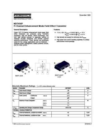
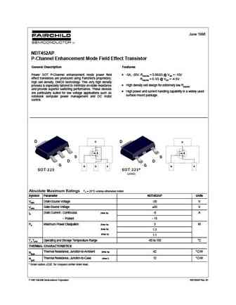
December 1998 NDT456P P-Channel Enhancement Mode Field Effect Transistor General Description Features Power SOT P-Channel enhancement mode power field -7.5 A, -30 V. RDS(ON) = 0.030 @ VGS = -10 V effect transistors are produced using Fairchild's RDS(ON) = 0.045 @ VGS = -4.5 V. proprietary, high cell density, DMOS technology. This very high density process is especially tailo
ndt456p.pdf
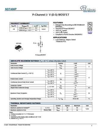
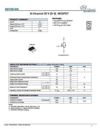
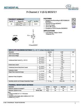
NDT456P www.VBsemi.tw P-Channel 35 V (D-S) MOSFET FEATURES PRODUCT SUMMARY Halogen-free According to IEC 61249-2-21 VDS (V) RDS(on) ( ) ID (A)d Qg (Typ.) Definition 0.050 at VGS = - 10 V - 6.2 TrenchFET Power MOSFET - 35 9.8 nC 0.060 at VGS = - 4.5 V - 5.1 100 % Rg Tested 100 % UIS Tested Compliant to RoHS Directive 2002/95/EC S APPLICATIONS Load S
ndt451an.pdf
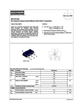
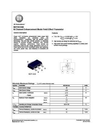
February 2009 NDT451AN N-Channel Enhancement Mode Field Effect Transistor General Description Features Power SOT N-Channel enhancement mode power field 7.2A, 30V. RDS(ON) = 0.035 @ VGS = 10V effect transistors are produced using Fairchild's RDS(ON) = 0.05 @ VGS = 4.5V. proprietary, high cell density, DMOS technology. This very high density process is especially tailored to mini
ndt454p.pdf
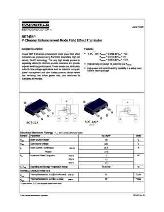
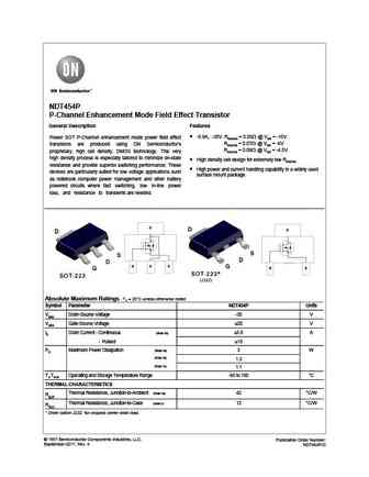
June 1996 NDT454P P-Channel Enhancement Mode Field Effect Transistor General Description Features -5.9A, -30V. RDS(ON) = 0.05 @ VGS = -10V Power SOT P-Channel enhancement mode power field effect RDS(ON) = 0.07 @ VGS = -6V transistors are produced using Fairchild's proprietary, high cell RDS(ON) = 0.09 @ VGS = -4.5V. density, DMOS technology. This very high density process is


Другие IGBT... NDT410EL, NDT451AN, NDT451N, NDT452AP, NDT452P, NDT453N, NDT454P, NDT455N, IRFP460, OM11N55SA, OM11N60SA, OM1N100SA, OM1N100ST, OM3N100SA, OM3N100ST, OM5N100SA, OM6N100SA
Параметры MOSFET. Взаимосвязь и компромиссы
🌐 : EN ES РУ

Список транзисторов
Обновления
MOSFET: MSQ60P04D | MSQ40P07D | MSQ30P40D | MSQ30P15 | MSQ30P07D | MSQ100N03D | MSHM60P14 | MSHM40N085 | MSHM30N46 | MSH60N35D | MSH40N032 | MSH30P100 | MSH100N045SA | MSD60P16 | MSD40P45 | MSB100N023
Popular searches
d882 datasheet | tip29 transistor | s9014 transistor datasheet | 2sa1491 | 2sc1313 datasheet | 2sc984 | 2sa872 | 2sc1222