P5N50C datasheet, аналоги, основные параметры
Наименование производителя: P5N50C 📄📄
Тип транзистора: MOSFET
Полярность: N
Предельные значения
Pd ⓘ
- Максимальная рассеиваемая мощность: 98.4 W
|Vds|ⓘ - Максимально допустимое напряжение сток-исток: 500 V
|Vgs|ⓘ - Максимально допустимое напряжение затвор-исток: 30 V
|Id| ⓘ - Максимально допустимый постоянный ток стока: 5 A
Tj ⓘ - Максимальная температура канала: 150 °C
Электрические характеристики
tr ⓘ -
Время нарастания: 49 ns
Cossⓘ - Выходная емкость: 75 pf
RDSonⓘ - Сопротивление сток-исток открытого транзистора: 1.5 Ohm
Тип корпуса: TO-220
Аналог (замена) для P5N50C
- подборⓘ MOSFET транзистора по параметрам
P5N50C даташит
..1. Size:890K thinkisemi
p5n50c.pdf 
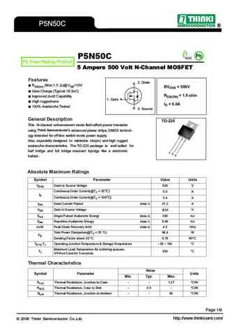
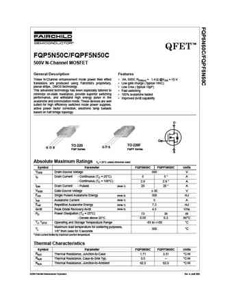
P5N50C Pb P5N50C Pb Free Plating Product 5 Ampere 500 Volt N-Channel MOSFET Features 2. Drain RDS(on) (Max 1.5 )@VGS=10V BVDSS = 500V Gate Charge (Typical 18.5nC) RDS(ON) = 1.5 ohm Improved dv/dt Capability 1. Gate High ruggedness ID = 5.0A 100% Avalanche Tested 3. Source General Description TO-220 This N-channel en
0.2. Size:979K onsemi
fqp5n50c fqpf5n50c.pdf 
Is Now Part of To learn more about ON Semiconductor, please visit our website at www.onsemi.com ON Semiconductor and the ON Semiconductor logo are trademarks of Semiconductor Components Industries, LLC dba ON Semiconductor or its subsidiaries in the United States and/or other countries. ON Semiconductor owns the rights to a number of patents, trademarks, copyrights, trade secrets, and oth
9.2. Size:265K fairchild semi
fdp5n50 fdpf5n50.pdf 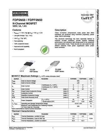
December 2007 UniFETTM FDP5N50 / FDPF5N50 tm N-Channel MOSFET 500V, 5A, 1.4 Features Description RDS(on) = 1.15 ( Typ.)@ VGS = 10V, ID = 2.5A These N-Channel enhancement mode power field effect transistors are produced using Fairchild s proprietary, planar Low gate charge ( Typ. 11nC) stripe, DMOS technology. Low Crss ( Typ. 5pF) This advanced technology has bee
9.3. Size:371K fairchild semi
fdp5n50.pdf 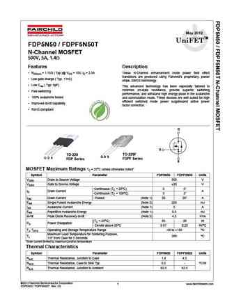
May 2012 UniFETTM FDP5N50 / FDPF5N50T tm N-Channel MOSFET 500V, 5A, 1.4 Features Description RDS(on) = 1.15 ( Typ.)@ VGS = 10V, ID = 2.5A These N-Channel enhancement mode power field effect transistors are produced using Fairchild s proprietary, planar Low gate charge ( Typ. 11nC) stripe, DMOS technology. Low Crss ( Typ. 5pF) This advanced technology has been es
9.4. Size:247K fairchild semi
fdp5n50nz fdpf5n50nz.pdf 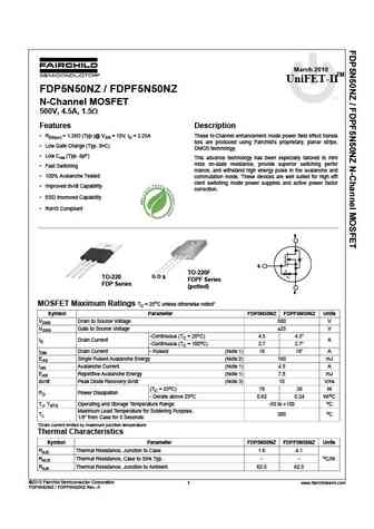
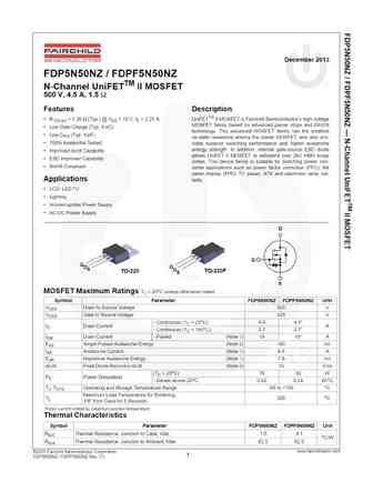
March 2010 UniFET-IITM FDP5N50NZ / FDPF5N50NZ tm N-Channel MOSFET 500V, 4.5A, 1.5 Features Description RDS(on) = 1.38 (Typ.)@ VGS = 10V, ID = 2.25A These N-Channel enhancement mode power field effect transis tors are produced using Fairchild s proprietary, planar stripe, Low Gate Charge (Typ. 9nC) DMOS technology. Low Crss (Typ. 4pF) This advance technology has b
9.5. Size:256K fairchild semi
fdp5n50nzf fdpf5n50nzf.pdf 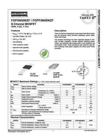
February 2010 TM UniFET-II FDP5N50NZF / FDPF5N50NZF tm N-Channel MOSFET 500V, 4.2A, 1.75 Features Description RDS(on) = 1.57 ( Typ.)@ VGS = 10V, ID = 2.1A These N-Channel enhancement mode power field effect transis- tors are produced using Fairchild s proprietary, planar stripe, Low Gate Charge ( Typ. 9nC) DMOS technology. Low Crss ( Typ. 4pF) This advanc
9.6. Size:427K fairchild semi
fdp5n50f fdpf5n50ft.pdf 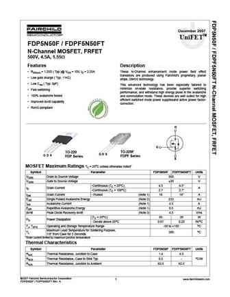
December 2007 UniFETTM FDP5N50F / FDPF5N50FT tm N-Channel MOSFET, FRFET 500V, 4.5A, 1.55 Features Description RDS(on) = 1.25 ( Typ.)@ VGS = 10V, ID = 2.25A These N-Channel enhancement mode power field effect transistors are produced using Fairchild s proprietary, planar Low gate charge ( Typ. 11nC) stripe, DMOS technology. Low Crss ( Typ. 5pF) This advanced tech
9.7. Size:224K fairchild semi
fdp5n50u fdpf5n50ut.pdf 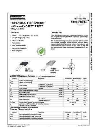
November2009 TM Ultra FRFET FDP5N50U / FDPF5N50UT tm N-Channel MOSFET, FRFET 500V, 4A, 2.0 Features Description RDS(on) = 1.65 ( Typ.)@ VGS = 10V, ID = 2A These N-Channel enhancement mode power field effect transis- tors are produced using Fairchild s proprietary, planar stripe, Low gate charge ( Typ. 11nC) DOMS technology. Low Crss ( Typ. 5pF) This advance tech
9.8. Size:702K fairchild semi
fdp5n50nzu fdpf5n50nzu.pdf 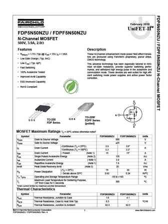
February 2010 TM UniFET-II FDP5N50NZU / FDPF5N50NZU tm N-Channel MOSFET 500V, 3.9A, 2.0 Features Description RDS(on) = 1.7 ( Typ.)@ VGS = 10V, ID = 1.95A These N-Channel enhancement mode power field effect transis- tors are produced using Fairchild s proprietary, planar stripe, Low Gate Charge ( Typ. 9nC) DMOS technology. Low Crss ( Typ. 4pF) This advance
9.9. Size:212K vishay
sihp5n50d.pdf 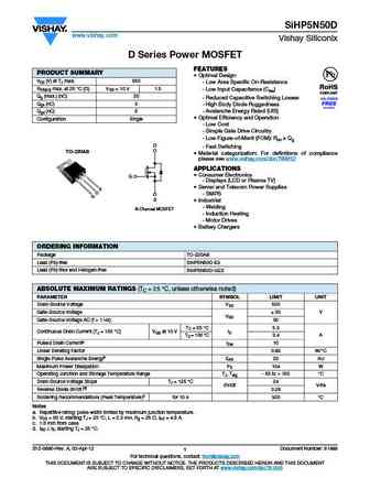
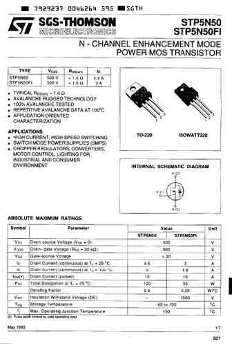
SiHP5N50D www.vishay.com Vishay Siliconix D Series Power MOSFET FEATURES PRODUCT SUMMARY Optimal Design VDS (V) at TJ max. 550 - Low Area Specific On-Resistance RDS(on) max. at 25 C ( ) VGS = 10 V 1.5 - Low Input Capacitance (Ciss) Qg (max.) (nC) 20 - Reduced Capacitive Switching Losses Qgs (nC) 3 - High Body Diode Ruggedness Qgd (nC) 5 - Avalanche Energy Rated (UIS)
9.10. Size:164K ixys
ixfa5n50p3 ixfp5n50p3 ixfy5n50p3.pdf 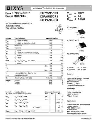
Advance Technical Information Polar3 TM HiPerFETTM VDSS = 500V IXFY5N50P3 Power MOSFETs ID25 = 5A IXFA5N50P3 RDS(on) 1.65 IXFP5N50P3 N-Channel Enhancement Mode Avalanche Rated TO-252 (IXFY) Fast Intrinsic Rectifier G S D (Tab) Symbol Test Conditions Maximum Ratings VDSS TJ = 25 C to 150 C 500 V TO-263 AA (IXFA) VDGR TJ = 25 C to 150 C, R
9.12. Size:1034K magnachip
mdf5n50zth mdp5n50zth.pdf 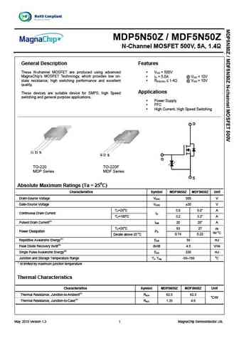
MDP5N50Z / MDF5N50Z N-Channel MOSFET 500V, 5A, 1.4 General Description Features These N-channel MOSFET are produced using advanced V = 500V DS MagnaChip s MOSFET Technology, which provides low on- I = 5.0A @ V = 10V D GS state resistance, high switching performance and excellent R 1.4 @ V = 10V DS(ON) GS quality. Applications These devices are suitable device fo
9.13. Size:1047K magnachip
mdf5n50fth mdp5n50fth.pdf 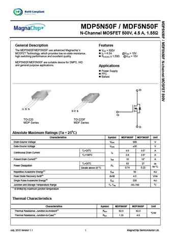
MDP5N50F / MDF5N50F N-Channel MOSFET 500V, 4.5 A, 1.55 General Description Features The MDP5N50F/MDF5N50F use advanced Magnachip s V = 500V DS MOSFET Technology, which provides low on-state resistance, I = 4.5A @V = 10V D GS high switching performance and excellent quality. RDS(ON) 1.55 @VGS = 10V MDP5N50F/MDF5N50F are suitable device for SMPS, HID and genera
9.14. Size:1146K magnachip
mdf5n50bth mdp5n50bth.pdf 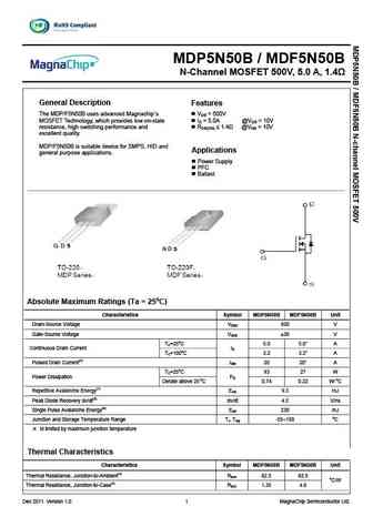
MDP5N50B / MDF5N50B N-Channel MOSFET 500V, 5.0 A, 1.4 General Description Features The MDP/F5N50B uses advanced Magnachip s VDS = 500V MOSFET Technology, which provides low on-state ID = 5.0A @VGS = 10V resistance, high switching performance and RDS(ON) 1.4 @VGS = 10V excellent quality. MDP/F5N50B is suitable device for SMPS, HID and Applications general purpose
9.15. Size:1197K magnachip
mdp5n50th.pdf 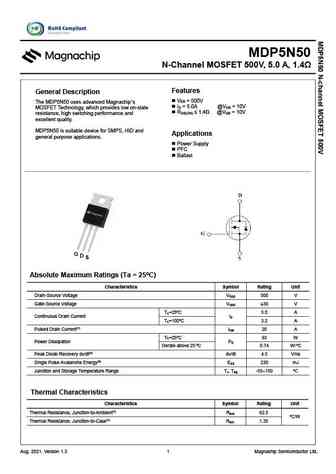
MDP5N50 N-Channel MOSFET 500V, 5.0 A, 1.4 Features General Description V = 500V DS The MDP5N50 uses advanced Magnachip s I = 5.0A @V = 10V D GS MOSFET Technology, which provides low on-state R 1.4 @V = 10V DS(ON) GS resistance, high switching performance and excellent quality. MDP5N50 is suitable device for SMPS, HID and Applications gener
9.16. Size:762K winsemi
wfp5n50.pdf 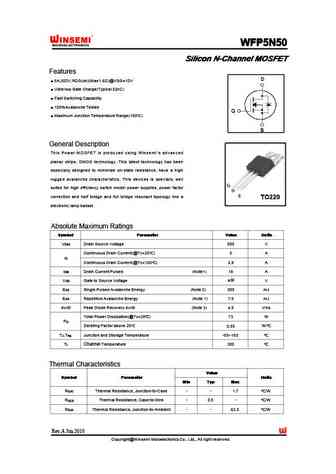
WFP5N50 WFP5N50 WFP5N50 WFP5N50 Silicon N-Channel MOSFET Silicon N-Channel MOSFET Silicon N-Channel MOSFET Silicon N-Channel MOSFET Features 5A,500V,RDS(on)(Max1.6 )@VGS=10V Ultra-low Gate Charge(Typical 32nC) Fast Switching Capability 100%Avalanche Tested Maximum Junction Temperature Range(150 ) General Description This Power MO SFET is pro du ced using Wi
9.17. Size:735K winsemi
sfp5n50.pdf 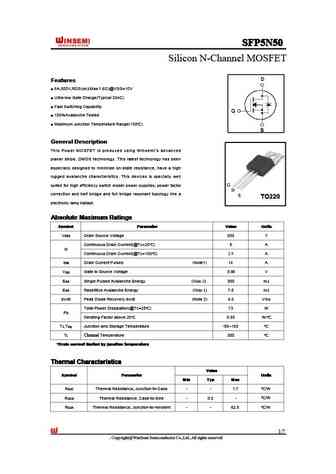
SFP5N50 SFP5N50 SFP5N50 SFP5N50 Silicon N-Channel MOSFET Features Features Features Features 5A,500V,RDS(on)(Max 1.6 )@VGS=10V Ultra-low Gate Charge(Typical 32nC) Fast Switching Capability 100%Avalanche Tested Maximum Junction Temperature Range(150 ) General Description General Description General Description General Description This Power MOSFET is prod
9.18. Size:1128K maple semi
slp5n50s slf5n50s.pdf 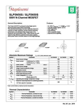
LEAD FREE Pb RoHS SLP5N50S / SLF5N50S 500V N-Channel MOSFET General Description Features This Power MOSFET is produced using Maple semi s - 5A, 500V, RDS(on) typ. = 1.12 @VGS = 10 V advanced planar stripe DMOS technology. - Low gate charge ( typical 22 nC) This advanced technology has been especially tailored to - High ruggedness minimize on-state resistance, provide superi
9.19. Size:203K semihow
hfp5n50s.pdf 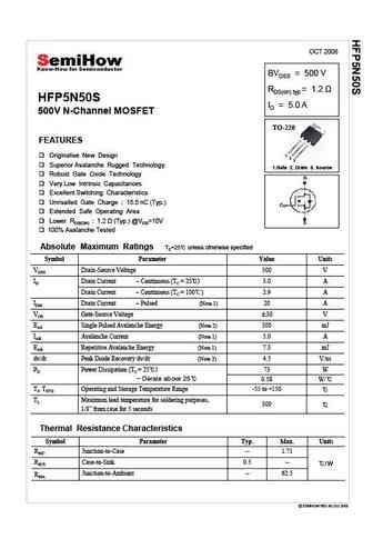
OCT 2008 BVDSS = 500 V RDS(on) typ HFP5N50S ID = 5.0 A 500V N-Channel MOSFET TO-220 FEATURES 1 Originative New Design 2 3 Superior Avalanche Rugged Technology 1.Gate 2. Drain 3. Source Robust Gate Oxide Technology Very Low Intrinsic Capacitances Excellent Switching Characteristics Unrivalled Gate Charge 15.5 nC (Typ.) Extended Safe Operating Area Lower RD
9.20. Size:203K semihow
hfp5n50u.pdf 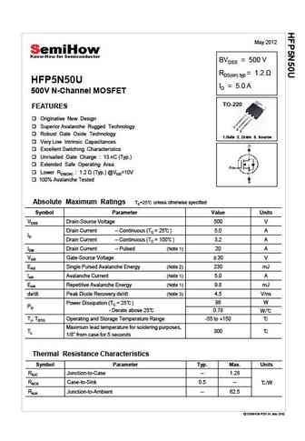
May 2012 BVDSS = 500 V RDS(on) typ HFP5N50U ID = 5.0 A 500V N-Channel MOSFET TO-220 FEATURES Originative New Design Superior Avalanche Rugged Technology 1 2 3 Robust Gate Oxide Technology 1.Gate 2. Drain 3. Source Very Low Intrinsic Capacitances Excellent Switching Characteristics Unrivalled Gate Charge 13 nC (Typ.) Extended Safe Operating Area Low
9.21. Size:354K trinnotech
tmp5n50sg tmpf5n50sg.pdf 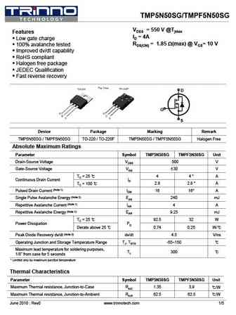
TMP5N50SG/TMPF5N50SG VDSS = 550 V @Tjmax Features ID = 4A Low gate charge RDS(ON) = 1.85 W(max) @ VGS= 10 V 100% avalanche tested Improved dv/dt capability RoHS compliant Halogen free package JEDEC Qualification Fast reverse recovery D G S Device Package Marking Remark TMP5N50SG / TMPF5N50SG TO-220 / TO-220F TMP5N50SG / TMPF5N50SG Halogen Free Abs
9.22. Size:347K trinnotech
tmp5n50 tmpf5n50.pdf 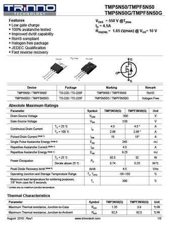
TMP5N50/TMPF5N50 TMP5N50G/TMPF5N50G Features VDSS = 550 V @Tjmax Low gate charge ID = 4.5A 100% avalanche tested RDS(ON) = 1.65 W(max) @ VGS= 10 V Improved dv/dt capability RoHS compliant Halogen free package JEDEC Qualification Fast reverse recovery D G S Device Package Marking Remark TMP5N50 / TMPF5N50 TO-220 / TO-220F TMP5N50 / TMPF5N50 RoHS T
9.25. Size:241K cn minos
mp5n50.pdf 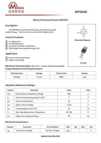
Silicon N-Channel Power MOSFET Description The MP5N50 uses advanced technology and design to provide excellent R . It can be used in a wide variety of applications. DS(ON) General Features Schematic diagram V =500V,I =5A DS D Low ON Resistance Low Reverse transfer capacitances 100% Single Pulse avalanche energy Test Application Power switching application A
9.26. Size:287K inchange semiconductor
mdp5n50bth.pdf 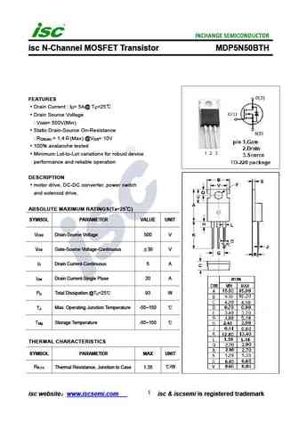
isc N-Channel MOSFET Transistor MDP5N50BTH FEATURES Drain Current I = 5A@ T =25 D C Drain Source Voltage V = 500V(Min) DSS Static Drain-Source On-Resistance R = 1.4 (Max) @V = 10V DS(on) GS 100% avalanche tested Minimum Lot-to-Lot variations for robust device performance and reliable operation DESCRIPTION motor drive, DC-DC converter, power switch and soleno
9.27. Size:287K inchange semiconductor
mdp5n50th.pdf 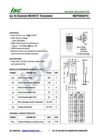
isc N-Channel MOSFET Transistor MDP5N50TH FEATURES Drain Current I = 5A@ T =25 D C Drain Source Voltage V = 500V(Min) DSS Static Drain-Source On-Resistance R = 1.4 (Max) @V = 10V DS(on) GS 100% avalanche tested Minimum Lot-to-Lot variations for robust device performance and reliable operation DESCRIPTION motor drive, DC-DC converter, power switch and solenoi
9.28. Size:1600K cn apm
ap5n50d.pdf 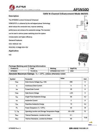
AP5N50D 500V N-Channel Enhancement Mode MOSFE Description The AP5N50D is silicon N-channel Enhanced VDMOSFETs, is obtained by the self-aligned planar Technology which reduce the conduction loss, improve switching performance and enhance the avalanche energy. The transistor can be used in various power switching circuit for system miniaturization and higher efficiency. General
9.29. Size:1440K cn apm
ap5n50f ap5n50p ap5n50t.pdf 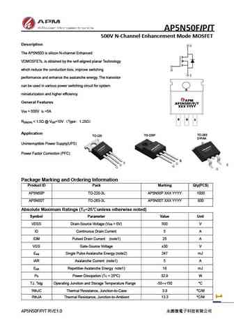
AP5N50FIPIT 500V N-Channel Enhancement Mode MOSFET Description The AP5N50D is silicon N-channel Enhanced VDMOSFETs, is obtained by the self-aligned planar Technology which reduce the conduction loss, improve switching performance and enhance the avalanche energy. The transistor can be used in various power switching circuit for system miniaturization and higher efficiency. Ge
9.30. Size:1342K cn apm
ap5n50bd.pdf 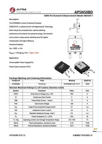
AP5N50BD 500V N-Channel Enhancement Mode MOSFET Description The AP5N50BD is silicon N-channel Enhanced VDMOSFETs, is obtained by the self-aligned planar Technology which reduce the conduction loss, improve switching performance and enhance the avalanche energy. The transistor can be used in various power switching circuit for system miniaturization and higher efficiency. Gene
Другие IGBT... OM60N10SC, OM6101ST, OM6104ST, OM6105SC, OM6106SC, P50B4EA, P50B6EA, P55NF06, IRF730, P9B40HP2, PCP1302, PCP1402, PCP1403, PCP1405, PDM6T20V3, PDM6UT20V08E, PDNM6T20V7E