APT30N60KC6. Аналоги и основные параметры
Наименование производителя: APT30N60KC6
Тип транзистора: MOSFET
Полярность: N
Предельные значения
Pd ⓘ - Максимальная рассеиваемая мощность: 219 W
|Vds|ⓘ - Максимально допустимое напряжение сток-исток: 600 V
|Vgs|ⓘ - Максимально допустимое напряжение затвор-исток: 20 V
|Id| ⓘ - Максимально допустимый постоянный ток стока: 30 A
Tj ⓘ - Максимальная температура канала: 150 °C
Электрические характеристики
tr ⓘ - Время нарастания: 17 ns
Cossⓘ - Выходная емкость: 1990 pf
RDSonⓘ - Сопротивление сток-исток открытого транзистора: 0.125 Ohm
Тип корпуса: TO-220
Аналог (замена) для APT30N60KC6
- подборⓘ MOSFET транзистора по параметрам
APT30N60KC6 даташит
apt30n60kc6.pdf
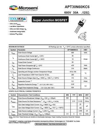
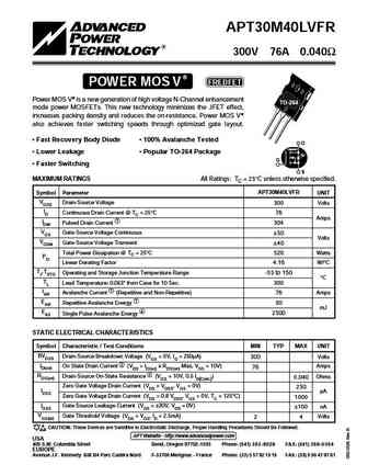
APT30N60KC6 600V 30A .125 COOLMOS Power Semiconductors Super Junction MOSFET TO-220 Ultra Low RDS(ON) Low Miller Capacitance Ultra Low Gate Charge, Qg Avalanche Energy Rated D Extreme dv/dt Rated G S MAXIMUM RATINGS All Ratings per die TC = 25 C unless otherwise specified. Symbol Parameter APT30N60KC6 UNIT 600 Volts VDSS Drain-Source Voltage 30
apt30n60bc6 apt30n60sc6.pdf
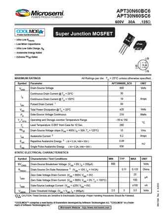
APT30N60BC6 APT30N60SC6 600V 30A .125 COOLMOS Power Semiconductors Super Junction MOSFET Ultra Low RDS(ON) D3PAK Low Miller Capacitance Ultra Low Gate Charge, Qg Avalanche Energy Rated Extreme dv/dt Rated D G S MAXIMUM RATINGS All Ratings per die TC = 25 C unless otherwise specified. Symbol Parameter APT30N60B_SC6 UNIT 600 Volts VDSS Drain-Sour
apt30n60bc6.pdf
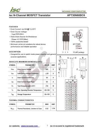
isc N-Channel MOSFET Transistor APT30N60BC6 FEATURES Drain Current I =30A@ T =25 D C Drain Source Voltage- V =600V(Min) DSS Static Drain-Source On-Resistance R =0.125 (Max) DS(on) 100% avalanche tested Minimum Lot-to-Lot variations for robust device performance and reliable operation DESCRIPTION Designed for use in switch mode power supplies and general pur
apt30gn60bg.pdf

TYPICAL PERFORMANCE CURVES APT30GN60B(G) 600V APT30GN60B APT30GN60BG* *G Denotes RoHS Compliant, Pb Free Terminal Finish. Utilizing the latest Field Stop and Trench Gate technologies, these IGBT's have ultra low VCE(ON) and are ideal for low frequency applications that require absolute minimum conduction loss. Easy paralleling is a result of very tight parameter distribution and
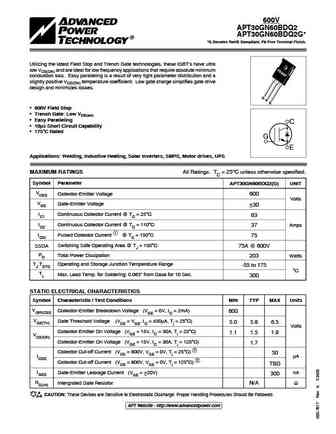
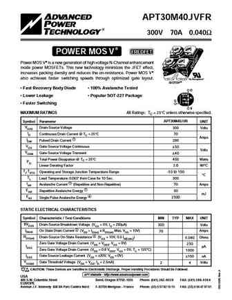
apt30m40b2vfrg.pdf
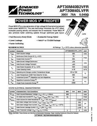
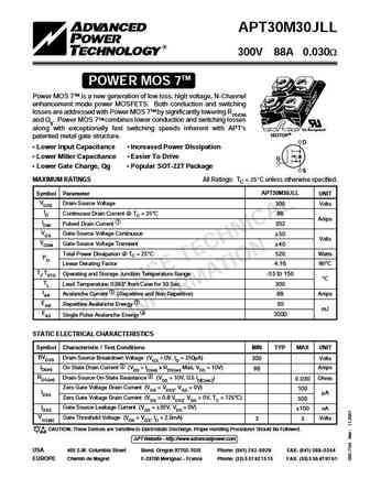
APT30M40B2VFR APT30M40LVFR 300V 76A 0.040 B2VFR POWER MOS V FREDFET T-MAX TO-264 Power MOS V is a new generation of high voltage N-Channel enhancement mode power MOSFETs. This new technology minimizes the JFET effect, increases packing density and reduces the on-resistance. Power MOS V also achieves faster switching speeds through optimized gate layout
apt30gf60ju3.pdf
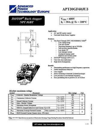
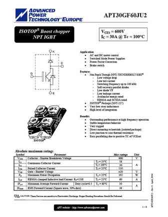
APT30GF60JU3 ISOTOP Buck chopper VCES = 600V IC = 30A @ Tc = 100 C NPT IGBT C Application AC and DC motor control Switched Mode Power Supplies G Features Non Punch Through (NPT) THUNDERBOLT IGBT - Low voltage drop - Low tail current E - Switching frequency up to 100 kHz - Soft recovery parallel diodes - Low diode VF - Low leakage current - Avalanch
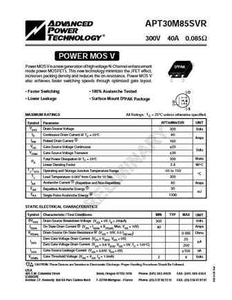
apt30m85.pdf

APT30M85BVFR 300V 40A 0.085 POWER MOS V FREDFET Power MOS V is a new generation of high voltage N-Channel enhancement TO-247 mode power MOSFETs. This new technology minimizes the JFET effect, increases packing density and reduces the on-resistance. Power MOS V also achieves faster switching speeds through optimized gate layout. Fast Recovery Body Diode 100% Avalanche Tes
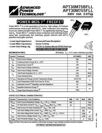
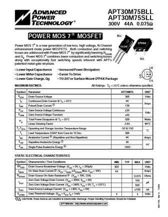
apt30m75bll.pdf

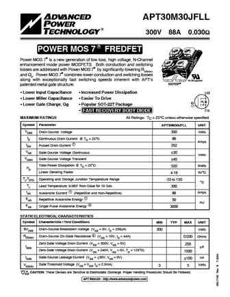
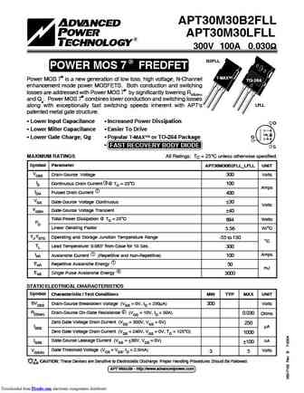
APT30M75BLL APT30M75SLL 300V 44A 0.075W TM BLL POWER MOS 7 Power MOS 7TM is a new generation of low loss, high voltage, N-Channel D3PAK TO-247 enhancement mode power MOSFETS. Both conduction and switching losses are addressed with Power MOS 7TM by significantly lowering RDS(ON) and Qg. Power MOS 7TM combines lower conduction and switching losses along with exceptionally fast switchin
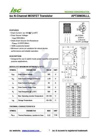
apt30m36b2fll apt30m36lfll.pdf
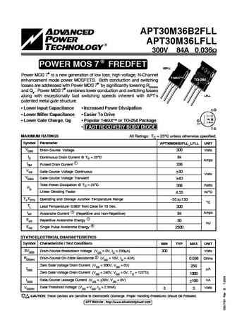
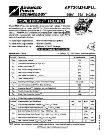
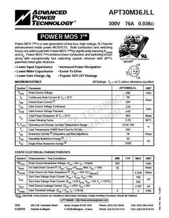
APT30M36B2FLL APT30M36LFLL 300V 84A 0.036 R FREDFET POWER MOS 7 FREDFET B2FLL Power MOS 7 is a new generation of low loss, high voltage, N-Channel T-MAX TO-264 enhancement mode power MOSFETS. Both conduction and switching losses are addressed with Power MOS 7 by significantly lowering RDS(ON) and Qg. Power MOS 7 combines lower conduction and switchin
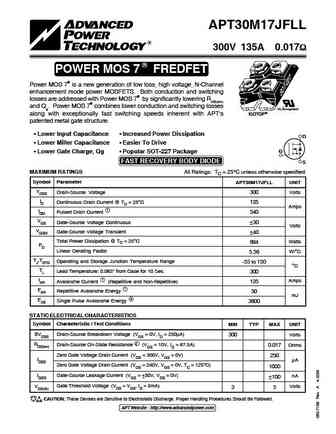
apt30m17jll.pdf
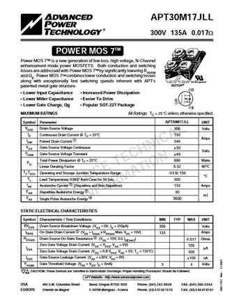
APT30M17JLL 300V 135A 0.017W TM POWER MOS 7 Power MOS 7TM is a new generation of low loss, high voltage, N-Channel enhancement mode power MOSFETS. Both conduction and switching losses are addressed with Power MOS 7TM by significantly lowering RDS(ON) and Qg. Power MOS 7TM combines lower conduction and switching losses along with exceptionally fast switching speeds inherent with APT's
apt30gn60bdq2g.pdf
TYPICAL PERFORMANCE CURVES APT30GN60BDQ2(G) 600V APT30GN60BDQ2 APT30GN60BDQ2G* *G Denotes RoHS Compliant, Pb Free Terminal Finish. Utilizing the latest Field Stop and Trench Gate technologies, these IGBT's have ultra low VCE(ON) and are ideal for low frequency applications that require absolute minimum conduction loss. Easy paralleling is a result of very tight parameter distrib
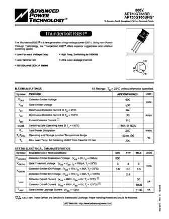
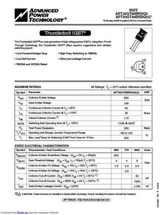
apt30gt60cr.pdf
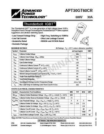
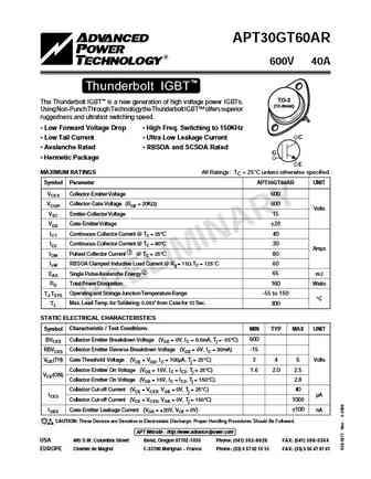
APT30GT60CR 600V 30A Thunderbolt IGBT TO-254 TO-254 The Thunderbolt IGBT is a new generation of high voltage power IGBTs. Using Non-Punch Through Technology the Thunderbolt IGBT offers superior ruggedness and ultrafast switching speed. Low Forward Voltage Drop High Freq. Switching to 150KHz C C Low Tail Current Ultra Low Leakage Current E G Avalanche R
apt30m75bfllg apt30m75sfllg.pdf
APT30M75BFLL APT30M75SFLL 300V 44A 0.075 BFLL R POWER MOS 7 FREDFET D3PAK Power MOS 7 is a new generation of low loss, high voltage, N-Channel TO-247 enhancement mode power MOSFETS. Both conduction and switching losses are addressed with Power MOS 7 by significantly lowering RDS(ON) and Qg. Power MOS 7 combines lower conduction and switching losses SFLL
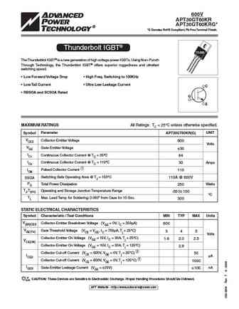
apt30m85svrg.pdf
APT30M85SVR 300V 40A 0.085 POWER MOS V Power MOS V is a new generation of high voltage N-Channel enhancement D3PAK mode power MOSFETs. This new technology minimizes the JFET effect, increases packing density and reduces the on-resistance. Power MOS V also achieves faster switching speeds through optimized gate layout. Faster Switching 100% Avalanche Tested D Lower Lea
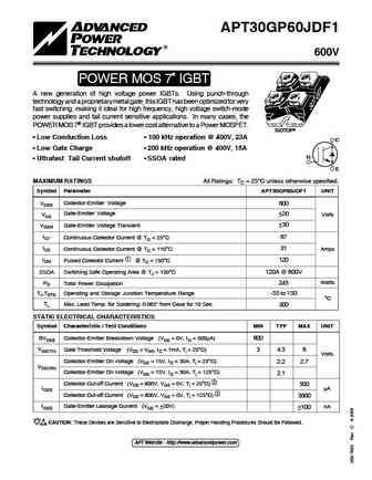
apt30gp60b.pdf

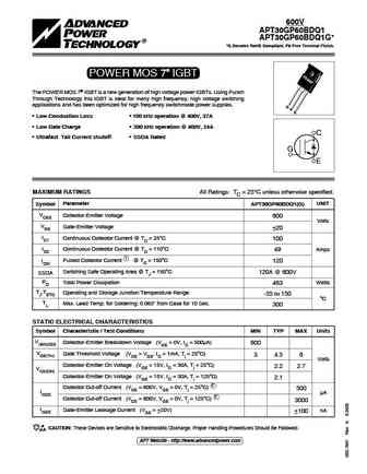
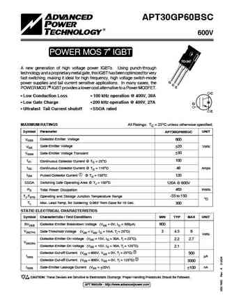
APT30GP60B 600V POWER MOS 7 IGBT A new generation of high voltage power IGBTs. Using punch-through TO-247 technology and a proprietary metal gate, this IGBT has been optimized for very fast switching, making it ideal for high frequency, high voltage switch- mode power supplies and tail current sensitive applications. In many cases, the POWER MOS 7 IGBT provides a lower cost alter
apt30gt60krg.pdf
TYPICAL PERFORMANCE CURVES APT30GT60KR(G) 600V APT30GT60KR APT30GT60KRG* *G Denotes RoHS Compliant, Pb Free Terminal Finish. Thunderbolt IGBT TO-220 The Thunderblot IGBT is a new generation of high voltage power IGBTs. Using Non- Punch Through Technology, the Thunderblot IGBT offers superior ruggedness and ultrafast switching speed. Low Forward Voltage Drop High
apt30gp60bdf1.pdf

TYPICAL PERFORMANCE CURVES APT30GP60BDF1 APT30GP60BDF1 600V POWER MOS 7 IGBT TO-247 A new generation of high voltage power IGBTs. Using punch-through technology and a proprietary metal gate, this IGBT has been optimized for very fast switching, making it ideal for high frequency, high voltage switch-mode G power supplies and tail current sensitive applications. In many cases, the
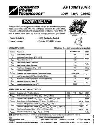
apt30m19jvfr.pdf
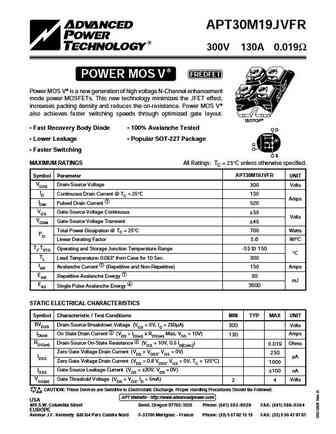
APT30M19JVFR 300V 130A 0.019 POWER MOS V FREDFET Power MOS V is a new generation of high voltage N-Channel enhancement mode power MOSFETs. This new technology minimizes the JFET effect, increases packing density and reduces the on-resistance. Power MOS V also achieves faster switching speeds through optimized gate layout. ISOTOP Fast Recovery Body Diode 100% Avalanche
apt30m36jfll.pdf
APT30M36JFLL 300V 76A 0.036 R POWER MOS 7 FREDFET Power MOS 7 is a new generation of low loss, high voltage, N-Channel enhancement mode power MOSFETS. Both conduction and switching losses are addressed with Power MOS 7 by significantly lowering RDS(ON) "UL Recognized" and Qg. Power MOS 7 combines lower conduction and switching losses ISOTOP along with e
apt30m40b2vr.pdf
APT30M40B2VR APT30M40LVR 300V 76A 0.040W B2VR POWER MOS V T-MAX Power MOS V is a new generation of high voltage N-Channel enhancement TO-264 mode power MOSFETs. This new technology minimizes the JFET effect, increases packing density and reduces the on-resistance. Power MOS V also achieves faster switching speeds through optimized gate layout.. LVR Faster Switching
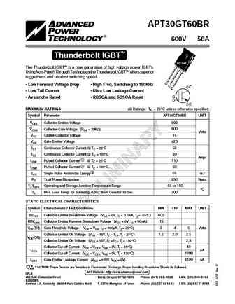
apt30gt60kr.pdf
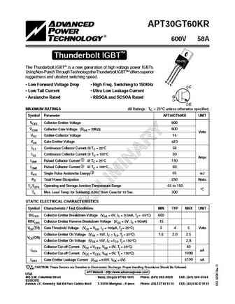
APT30GT60KR 600V 58A Thunderbolt IGBT TO-220 The Thunderbolt IGBT is a new generation of high voltage power IGBTs. Using Non-Punch Through Technology the Thunderbolt IGBT offers superior ruggedness and ultrafast switching speed. G C Low Forward Voltage Drop High Freq. Switching to 150KHz E C Low Tail Current Ultra Low Leakage Current Avalanche Rated
apt30m70bvr.pdf

APT30M70BVR 300V 48A 0.070 POWER MOS V Power MOS V is a new generation of high voltage N-Channel enhancement TO-247 mode power MOSFETs. This new technology minimizes the JFET effect, increases packing density and reduces the on-resistance. Power MOS V also achieves faster switching speeds through optimized gate layout. D Faster Switching 100% Avalanche Tested Lower
apt30gp60jdf1.pdf
TYPICAL PERFORMANCE CURVES APT30GP60JDF1 APT30GP60JDF1 600V POWER MOS 7 IGBT A new generation of high voltage power IGBTs. Using punch-through technology and a proprietary metal gate, this IGBT has been optimized for very fast switching, making it ideal for high frequency, high voltage switch-mode power supplies and tail current sensitive applications. In many cases, the "UL Recog
apt30gt60brd.pdf
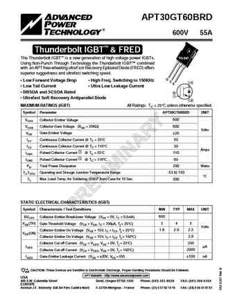
APT30GT60BRD 600V 55A Thunderbolt IGBT & FRED The Thunderbolt IGBT is a new generation of high voltage power IGBTs. TO-247 Using Non-Punch Through Technology the Thunderbolt IGBT combined with an APT free-wheeling ultraFast Recovery Epitaxial Diode (FRED) offers superior ruggedness and ultrafast switching speed. G Low Forward Voltage Drop High Freq. Switching to 150KHz
apt30m75bllg apt30m75sllg.pdf
APT30M75BLL APT30M75SLL 300V 44A 0.075 R BLL POWER MOS 7 MOSFET D3PAK Power MOS 7 is a new generation of low loss, high voltage, N-Channel TO-247 enhancement mode power MOSFETS. Both conduction and switching losses are addressed with Power MOS 7 by significantly lowering RDS(ON) and Qg. Power MOS 7 combines lower conduction and switching losses SLL alo
apt30m30b2llg apt30m30lllg.pdf
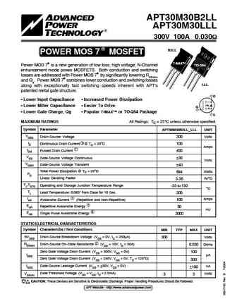
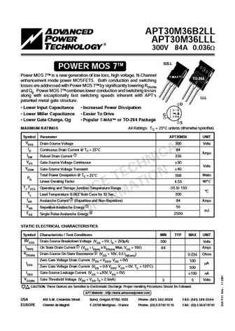
APT30M30B2LL APT30M30LLL 300V 100A 0.030 R B2LL POWER MOS 7 MOSFET T-MAX Power MOS 7 is a new generation of low loss, high voltage, N-Channel TO-264 enhancement mode power MOSFETS. Both conduction and switching losses are addressed with Power MOS 7 by significantly lowering RDS(ON) and Qg. Power MOS 7 combines lower conduction and switching losses LLL
apt30m36jll.pdf
APT30M36JLL 300V 76A 0.036W TM POWER MOS 7 Power MOS 7TM is a new generation of low loss, high voltage, N-Channel enhancement mode power MOSFETS. Both conduction and switching losses are addressed with Power MOS 7TM by significantly lowering RDS(ON) and Qg. Power MOS 7TM combines lower conduction and switching losses along with exceptionally fast switching speeds inherent with APT's "
apt30m61bll.pdf

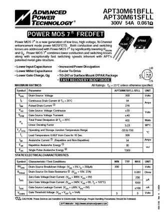
APT30M61BLL APT30M61SLL 300V 54A 0.061W TM BLL POWER MOS 7 Power MOS 7TM is a new generation of low loss, high voltage, N-Channel D3PAK TO-247 enhancement mode power MOSFETS. Both conduction and switching losses are addressed with Power MOS 7TM by significantly lowering RDS(ON) and Qg. Power MOS 7TM combines lower conduction and switching losses along with exceptionally fast switchin
apt30m85bvfr.pdf
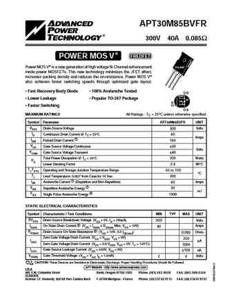
APT30M85BVFR 300V 40A 0.085 POWER MOS V FREDFET Power MOS V is a new generation of high voltage N-Channel enhancement TO-247 mode power MOSFETs. This new technology minimizes the JFET effect, increases packing density and reduces the on-resistance. Power MOS V also achieves faster switching speeds through optimized gate layout. Fast Recovery Body Diode 100% Avalanche Tes
apt30m85bvr.pdf

APT30M85BVR 300V 40A 0.085 POWER MOS V Power MOS V is a new generation of high voltage N-Channel enhancement TO-247 mode power MOSFETs. This new technology minimizes the JFET effect, increases packing density and reduces the on-resistance. Power MOS V also achieves faster switching speeds through optimized gate layout. Faster Switching 100% Avalanche Tested D Lower
apt30m36lll apt30m36b2ll.pdf
APT30M36B2LL APT30M36LLL 300V 84A 0.036W B2LL TM POWER MOS 7 Power MOS 7TM is a new generation of low loss, high voltage, N-Channel T-MAX TO-264 enhancement mode power MOSFETS. Both conduction and switching losses are addressed with Power MOS 7TM by significantly lowering RDS(ON) and Qg. Power MOS 7TM combines lower conduction and switching losses along with exceptionally fast s
apt30m40jvr.pdf

APT30M40JVR 300V 70A 0.040 POWER MOS V Power MOS V is a new generation of high voltage N-Channel enhancement mode power MOSFETs. This new technology minimizes the JFET effect, increases packing density and reduces the on-resistance. Power MOS V also achieves faster switching speeds through optimized gate layout. "UL Recognized" ISOTOP D Faster Switching 100% Avalanc
apt30gf60ju2.pdf
APT30GF60JU2 ISOTOP Boost chopper VCES = 600V IC = 30A @ Tc = 100 C NPT IGBT K Application AC and DC motor control Switched Mode Power Supplies Power Factor Correction C Brake switch Features G Non Punch Through (NPT) THUNDERBOLT IGBT - Low voltage drop - Low tail current - Switching frequency up to 100 kHz - Soft recovery parallel diodes -
apt30m30jll.pdf
APT30M30JLL 300V 88A 0.030W TM POWER MOS 7 Power MOS 7TM is a new generation of low loss, high voltage, N-Channel enhancement mode power MOSFETS. Both conduction and switching losses are addressed with Power MOS 7TM by significantly lowering RDS(ON) and Qg. Power MOS 7TM combines lower conduction and switching losses along with exceptionally fast switching speeds inherent with APT's "
apt30m36b2ll.pdf

APT30M36B2LL APT30M36LLL 300V 84A 0.036W B2LL TM POWER MOS 7 Power MOS 7TM is a new generation of low loss, high voltage, N-Channel T-MAX TO-264 enhancement mode power MOSFETS. Both conduction and switching losses are addressed with Power MOS 7TM by significantly lowering RDS(ON) and Qg. Power MOS 7TM combines lower conduction and switching losses along with exceptionally fast s
apt30m70bvfr.pdf

APT30M70BVFR 300V 48A 0.070 POWER MOS V FREDFET Power MOS V is a new generation of high voltage N-Channel enhancement TO-247 mode power MOSFETs. This new technology minimizes the JFET effect, increases packing density and reduces the on-resistance. Power MOS V also achieves faster switching speeds through optimized gate layout. Fast Recovery Body Diode 100% Avalanche Tes
apt30m30b2ll.pdf

APT30M30B2LL APT30M30LLL 300V 100A 0.030W B2LL TM POWER MOS 7 Power MOS 7TM is a new generation of low loss, high voltage, N-Channel T-MAX TO-264 enhancement mode power MOSFETS. Both conduction and switching losses are addressed with Power MOS 7TM by significantly lowering RDS(ON) and Qg. Power MOS 7TM combines lower conduction and switching losses along with exceptionally fast
apt30m30jfll.pdf
APT30M30JFLL 300V 88A 0.030 R POWER MOS 7 FREDFET Power MOS 7 is a new generation of low loss, high voltage, N-Channel enhancement mode power MOSFETS. Both conduction and switching losses are addressed with Power MOS 7 by significantly lowering RDS(ON) and Qg. Power MOS 7 combines lower conduction and switching losses along with exceptionally fast switching
apt30gp60bdq1g.pdf
TYPICAL PERFORMANCE CURVES APT30GP60BDQ1(G) 600V APT30GP60BDQ1 APT30GP60BDQ1G* *G Denotes RoHS Compliant, Pb Free Terminal Finish. POWER MOS 7 IGBT The POWER MOS 7 IGBT is a new generation of high voltage power IGBTs. Using Punch Through Technology this IGBT is ideal for many high frequency, high voltage switching applications and has been optimized for high frequency swi
apt30m90avr.pdf

APT30M90AVR 300V 33A 0.090 POWER MOS V TO-3 Power MOS V is a new generation of high voltage N-Channel enhancement mode power MOSFETs. This new technology minimizes the JFET effect, increases packing density and reduces the on-resistance. Power MOS V also achieves faster switching speeds through optimized gate layout. D Faster Switching 100% Avalanche Tested Lower
apt30gn60sg apt30gp60bg.pdf

APT30GP60B APT30GP60S 600V B POWER MOS 7 IGBT D3PAK A new generation of high voltage power IGBTs. Using punch-through technology and a proprietary metal gate, this IGBT has been optimized for S C very fast switching, making it ideal for high frequency, high voltage switch- G E mode power supplies and tail current sensitive applications. In many cases, the POWER MOS 7 IGBT pr
apt30gt60brg.pdf
TYPICAL PERFORMANCE CURVES APT30GT60BR(G) 600V APT30GT60BR APT30GT60BRG* *G Denotes RoHS Compliant, Pb Free Terminal Finish. Thunderbolt IGBT The Thunderblot IGBT is a new generation of high voltage power IGBTs. Using Non- Punch Through Technology, the Thunderblot IGBT offers superior ruggedness and ultrafast switching speed. G C E Low Forward Voltage Drop Hig
apt30m40b2vrg.pdf
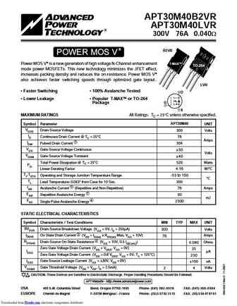
APT30M40B2VR APT30M40LVR 300V 76A 0.040W B2VR POWER MOS V T-MAX Power MOS V is a new generation of high voltage N-Channel enhancement TO-264 mode power MOSFETs. This new technology minimizes the JFET effect, increases packing density and reduces the on-resistance. Power MOS V also achieves faster switching speeds through optimized gate layout.. LVR Faster Switching
apt30gt60br.pdf
APT30GT60BR 600V 58A Thunderbolt IGBT TO-247 The Thunderbolt IGBT is a new generation of high voltage power IGBTs. Using Non-Punch Through Technology the Thunderbolt IGBT offers superior ruggedness and ultrafast switching speed. G Low Forward Voltage Drop High Freq. Switching to 150KHz C C E Low Tail Current Ultra Low Leakage Current Avalanche Rated
apt30m40lvfr.pdf
APT30M40LVFR 300V 76A 0.040 POWER MOS V FREDFET Power MOS V is a new generation of high voltage N-Channel enhancement TO-264 mode power MOSFETs. This new technology minimizes the JFET effect, increases packing density and reduces the on-resistance. Power MOS V also achieves faster switching speeds through optimized gate layout. Fast Recovery Body Diode 100% Avalanche Te
apt30m30b2fllg apt30m30lfll.pdf
APT30M30B2FLL APT30M30LFLL 300V 100A 0.030 R B2FLL POWER MOS 7 FREDFET T-MAX Power MOS 7 is a new generation of low loss, high voltage, N-Channel TO-264 enhancement mode power MOSFETS. Both conduction and switching losses are addressed with Power MOS 7 by significantly lowering RDS(ON) and Qg. Power MOS 7 combines lower conduction and switching losses
apt30gt60brdq2g.pdf
TYPICAL PERFORMANCE CURVES APT30GT60BRDQ2(G) 600V APT30GT60BRDQ2 APT30GT60BRDQ2G* *G Denotes RoHS Compliant, Pb Free Terminal Finish. Thunderbolt IGBT The Thunderblot IGBT is a new generation of high voltage power IGBTs. Using Non- Punch Through Technology, the Thunderblot IGBT offers superior ruggedness and ultrafast switching speed. G C E Low Forward Voltage Dro
apt30m61bfllg apt30m61sfllg.pdf
APT30M61BFLL APT30M61SFLL 300V 54A 0.061 R POWER MOS 7 FREDFET D3PAK Power MOS 7 is a new generation of low loss, high voltage, N-Channel TO-247 enhancement mode power MOSFETS. Both conduction and switching losses are addressed with Power MOS 7 by significantly lowering RDS(ON) and Qg. Power MOS 7 combines lower conduction and switching losses along with
apt30gp60bsc.pdf
TYPICAL PREFORMANCE CURVES APT30GP60BSC APT30GP60BSC 600V POWER MOS 7 IGBT TO-247 A new generation of high voltage power IGBTs. Using punch-through technology and a proprietary metal gate, this IGBT has been optimized for very fast switching, making it ideal for high frequency, high voltage switch-mode G power supplies and tail current sensitive applications. In many cases, the C
apt30m19jvr.pdf
APT30M19JVR 300V 130A 0.019 POWER MOS V Power MOS V is a new generation of high voltage N-Channel enhancement mode power MOSFETs. This new technology minimizes the JFET effect, increases packing density and reduces the on-resistance. Power MOS V also achieves faster switching speeds through optimized gate layout. "UL Recognized" ISOTOP Faster Switching 100% Avalanche
apt30m17jfll.pdf
APT30M17JFLL 300V 135A 0.017 R POWER MOS 7 FREDFET Power MOS 7 is a new generation of low loss, high voltage, N-Channel enhancement mode power MOSFETS. Both conduction and switching losses are addressed with Power MOS 7 by significantly lowering RDS(ON) and Qg. Power MOS 7 combines lower conduction and switching losses "UL Recognized" along with exceptiona
apt30f50b apt30f50s.pdf
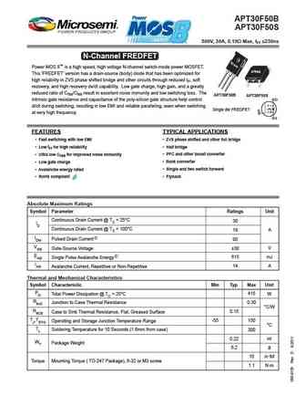
APT30F50B APT30F50S 500V, 30A, 0.19 Max, trr 230ns N-Channel FREDFET Power MOS 8 is a high speed, high voltage N-channel switch-mode power MOSFET. D3PAK This 'FREDFET' version has a drain-source (body) diode that has been optimized for high reliability in ZVS phase shifted bridge and other circuits through reduced trr, soft recovery, and high recovery dv/dt capability. Lo
apt30gs60srdq2g.pdf
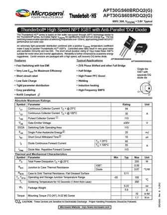
APT30GS60BRDQ2(G) APT30GS60SRDQ2(G) 600V, 30A, VCE(ON) = 2.8V Typical Thunderbolt High Speed NPT IGBT with Anti-Parallel 'DQ' Diode The Thunderbolt HS series is based on thin wafer non-punch through (NPT) technology similar to the Thunderbolt series, but trades higher VCE(ON) for significantly lower turn-on energy Eoff. The low switching losses enable operation at switching frequ
apt30gs60brdq2g.pdf

APT30GS60BRDQ2(G) APT30GS60SRDQ2(G) 600V, 30A, VCE(ON) = 2.8V Typical Thunderbolt High Speed NPT IGBT with Anti-Parallel 'DQ' Diode The Thunderbolt HS series is based on thin wafer non-punch through (NPT) technology similar to the Thunderbolt series, but trades higher VCE(ON) for significantly lower turn-on energy Eoff. The low switching losses enable operation at switching frequ
apt30gn60kg.pdf
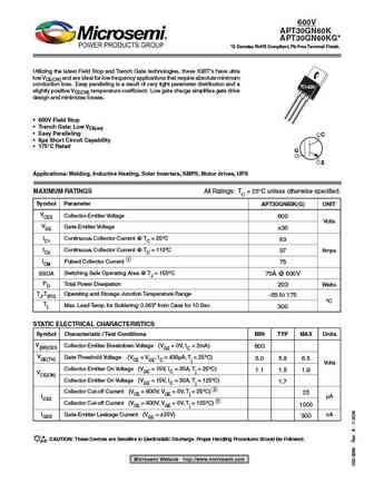
TYPICAL PERFORMANCE CURVES APT30GN60K(G) 600V APT30GN60K APT30GN60KG* *G Denotes RoHS Compliant, Pb Free Terminal Finish. Utilizing the latest Field Stop and Trench Gate technologies, these IGBT's have ultra low VCE(ON) and are ideal for low frequency applications that require absolute minimum conduction loss. Easy paralleling is a result of very tight parameter distribution and a
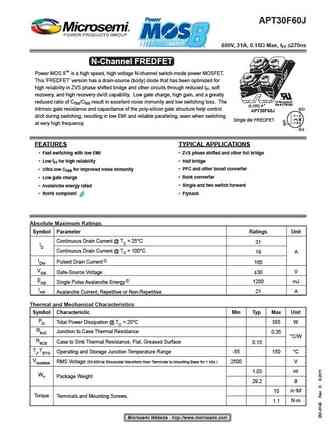
apt30m60j.pdf

APT30M60J 600V, 31A, 0.15 Max N-Channel MOSFET Power MOS 8 is a high speed, high voltage N-channel switch-mode power MOSFET. A proprietary planar stripe design yields excellent reliability and manufacturability. Low switching loss is achieved with low input capacitance and ultra low Crss "Miller" capaci- tance. The intrinsic gate resistance and capacitance of the poly-silicon ga
apt30f60j.pdf
APT30F60J 600V, 31A, 0.15 Max, trr 270ns N-Channel FREDFET Power MOS 8 is a high speed, high voltage N-channel switch-mode power MOSFET. This 'FREDFET' version has a drain-source (body) diode that has been optimized for high reliability in ZVS phase shifted bridge and other circuits through reduced trr, soft recovery, and high recovery dv/dt capability. Low gate charge, high
apt30gt60brdlg.pdf
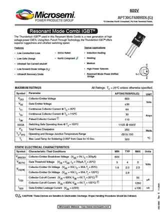
TYPICAL PERFORMANCE CURVES APT30GT60BRDL(G) 600V APT30GT60BRDL(G) *G Denotes RoHS Compliant, Pb Free Terminal Finish. Resonant Mode Combi IGBT The Thunderbolt IGBT used in this Resonant Mode Combi is a new generation of high voltage power IGBTs. Using Non- Punch Through Technology, the Thunderblot IGBT offers superior ruggedness and ultrafast switching speed. Typical Applicatio
apt30m36b2fll.pdf

isc N-Channel MOSFET Transistor APT30M36B2FLL FEATURES Drain Current I = 84A@ T =25 D C Drain Source Voltage- V =300V(Min) DSS Static Drain-Source On-Resistance R =0.036 (Max) DS(on) 100% avalanche tested Minimum Lot-to-Lot variations for robust device performance and reliable operation DESCRIPTION Designed for use in switch mode power supplies and general
apt30f50b.pdf

isc N-Channel MOSFET Transistor APT30F50B FEATURES Drain Current I = 30A@ T =25 D C Drain Source Voltage- V =500V(Min) DSS Static Drain-Source On-Resistance R = 0.19 (Max) DS(on) 100% avalanche tested Minimum Lot-to-Lot variations for robust device performance and reliable operation DESCRIPTION Designed for use in switch mode power supplies and general purp
apt30m75bll.pdf

isc N-Channel MOSFET Transistor APT30M75BLL FEATURES Drain Current I =44A@ T =25 D C Drain Source Voltage- V =300V(Min) DSS Static Drain-Source On-Resistance R =0.075 (Max) DS(on) 100% avalanche tested Minimum Lot-to-Lot variations for robust device performance and reliable operation DESCRIPTION Designed for use in switch mode power supplies and general pur
apt30m36lll.pdf
isc N-Channel MOSFET Transistor APT30M36LLL FEATURES Drain Current I = 84A@ T =25 D C Drain Source Voltage- V =300V(Min) DSS Static Drain-Source On-Resistance R =0.036 (Max) DS(on) 100% avalanche tested Minimum Lot-to-Lot variations for robust device performance and reliable operation DESCRIPTION Designed for use in switch mode power supplies and general pu
apt30m75bfll.pdf

isc N-Channel MOSFET Transistor APT30M75BFLL FEATURES Drain Current I = 44A@ T =25 D C Drain Source Voltage- V =300V(Min) DSS Static Drain-Source On-Resistance R =0.075 (Max) DS(on) 100% avalanche tested Minimum Lot-to-Lot variations for robust device performance and reliable operation DESCRIPTION Designed for use in switch mode power supplies and general p
apt30m70bvr.pdf

isc N-Channel MOSFET Transistor APT30M70BVR FEATURES Drain Current I =48A@ T =25 D C Drain Source Voltage- V =300V(Min) DSS Static Drain-Source On-Resistance R =0.07 (Max) DS(on) 100% avalanche tested Minimum Lot-to-Lot variations for robust device performance and reliable operation DESCRIPTION Designed for use in switch mode power supplies and general purp
apt30m30b2fll.pdf

isc N-Channel MOSFET Transistor APT30M30B2FLL FEATURES Drain Current I = 100A@ T =25 D C Drain Source Voltage- V =300V(Min) DSS Static Drain-Source On-Resistance R =0.03 (Max) DS(on) 100% avalanche tested Minimum Lot-to-Lot variations for robust device performance and reliable operation DESCRIPTION Designed for use in switch mode power supplies and general
apt30m36lfll.pdf

isc N-Channel MOSFET Transistor APT30M36LFLL FEATURES Drain Current I = 100A@ T =25 D C Drain Source Voltage- V =300V(Min) DSS Static Drain-Source On-Resistance R =0.03 (Max) DS(on) 100% avalanche tested Minimum Lot-to-Lot variations for robust device performance and reliable operation DESCRIPTION Designed for use in switch mode power supplies and general p
apt30m30lfll.pdf

isc N-Channel MOSFET Transistor APT30M30LFLL FEATURES Drain Current I = 100A@ T =25 D C Drain Source Voltage- V =300V(Min) DSS Static Drain-Source On-Resistance R =0.03 (Max) DS(on) 100% avalanche tested Minimum Lot-to-Lot variations for robust device performance and reliable operation DESCRIPTION Designed for use in switch mode power supplies and general p
apt30m61bll.pdf

isc N-Channel MOSFET Transistor APT30M61BLL FEATURES Drain Current I =54A@ T =25 D C Drain Source Voltage- V =300V(Min) DSS Static Drain-Source On-Resistance R =0.061 (Max) DS(on) 100% avalanche tested Minimum Lot-to-Lot variations for robust device performance and reliable operation DESCRIPTION Designed for use in switch mode power supplies and general pur
apt30m61bfll.pdf

isc N-Channel MOSFET Transistor APT30M61BFLL FEATURES Drain Current I = 54A@ T =25 D C Drain Source Voltage- V =300V(Min) DSS Static Drain-Source On-Resistance R =0.061 (Max) DS(on) 100% avalanche tested Minimum Lot-to-Lot variations for robust device performance and reliable operation DESCRIPTION Designed for use in switch mode power supplies and general p
apt30m85bvr.pdf

isc N-Channel MOSFET Transistor APT30M85BVR FEATURES Drain Current I =40A@ T =25 D C Drain Source Voltage- V =300V(Min) DSS Static Drain-Source On-Resistance R =0.085 (Max) DS(on) 100% avalanche tested Minimum Lot-to-Lot variations for robust device performance and reliable operation DESCRIPTION Designed for use in switch mode power supplies and general pur
apt30m36b2ll.pdf

isc N-Channel MOSFET Transistor APT30M36B2LL FEATURES Drain Current I = 84A@ T =25 D C Drain Source Voltage- V =300V(Min) DSS Static Drain-Source On-Resistance R =0.036 (Max) DS(on) 100% avalanche tested Minimum Lot-to-Lot variations for robust device performance and reliable operation DESCRIPTION Designed for use in switch mode power supplies and general p
apt30m70bvfr.pdf
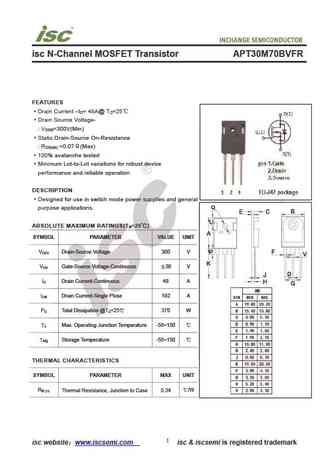
isc N-Channel MOSFET Transistor APT30M70BVFR FEATURES Drain Current I = 48A@ T =25 D C Drain Source Voltage- V =300V(Min) DSS Static Drain-Source On-Resistance R =0.07 (Max) DS(on) 100% avalanche tested Minimum Lot-to-Lot variations for robust device performance and reliable operation DESCRIPTION Designed for use in switch mode power supplies and general pu
apt30m30b2ll.pdf
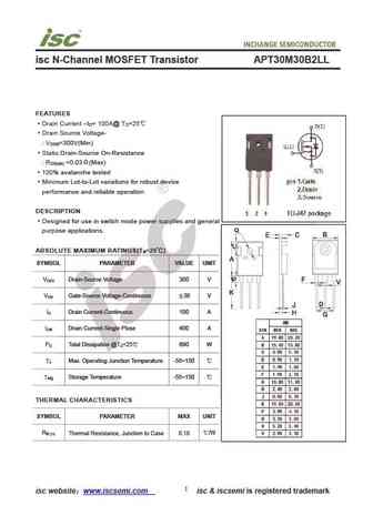
isc N-Channel MOSFET Transistor APT30M30B2LL FEATURES Drain Current I = 100A@ T =25 D C Drain Source Voltage- V =300V(Min) DSS Static Drain-Source On-Resistance R =0.03 (Max) DS(on) 100% avalanche tested Minimum Lot-to-Lot variations for robust device performance and reliable operation DESCRIPTION Designed for use in switch mode power supplies and general p
Другие IGBT... APT30M61BFLLG, APT30M61SFLLG, APT30M75BFLLG, APT30M75BLLG, APT30M75SFLLG, APT30M75SLLG, APT30M85SVRG, APT30N60BC6, IRFZ46N, APT30N60SC6, APT31M100B2, APT31M100L, APT31N60BCSG, APT31N60SCSG, APT32F120J, APT32M80J, APT33N90JCCU2
🌐 : EN ES РУ

Список транзисторов
Обновления
MOSFET: FTF30P35D | FTF25N35DHVT | FTF15N35D | FTE15C35G | FTP02P15G | FTE02P15G | AKF30N5P0SX | AKF30N10S | AKF20P45D | CM4407 | CM3407 | CM3400 | SVF11N65F | SVF11N65T | FKBB3105 | EHBA036R1
Popular searches
c2383 transistor | 2n3055 equivalent | s9015 datasheet | 2n6488 | 30j127 datasheet | 2sc1116a | 2sc460 | 2sc869 datasheet