APT5012JN. Аналоги и основные параметры
Наименование производителя: APT5012JN
Тип транзистора: MOSFET
Полярность: N
Предельные значения
Pd ⓘ - Максимальная рассеиваемая мощность: 520 W
|Vds|ⓘ - Максимально допустимое напряжение сток-исток: 500 V
|Vgs|ⓘ - Максимально допустимое напряжение затвор-исток: 30 V
|Id| ⓘ - Максимально допустимый постоянный ток стока: 43 A
Tj ⓘ - Максимальная температура канала: 150 °C
Электрические характеристики
tr ⓘ - Время нарастания: 25 ns
Cossⓘ - Выходная емкость: 1170 pf
RDSonⓘ - Сопротивление сток-исток открытого транзистора: 0.12 Ohm
Тип корпуса: SOT-227
Аналог (замена) для APT5012JN
- подборⓘ MOSFET транзистора по параметрам
APT5012JN даташит
apt5012jn.pdf
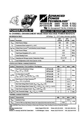
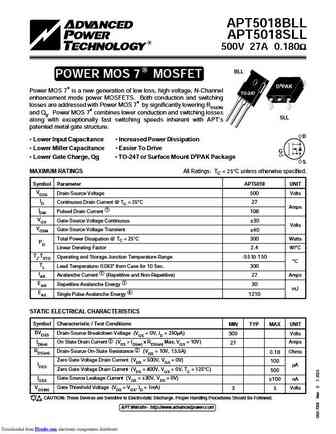
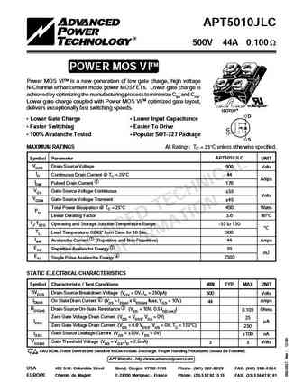
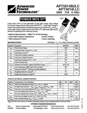
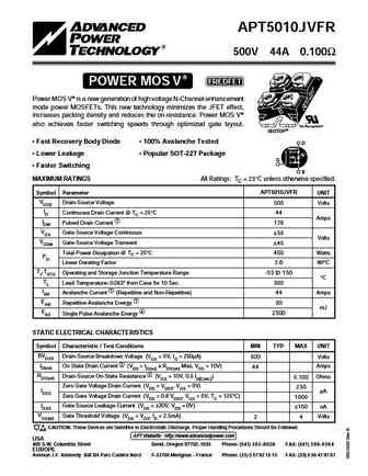
D G APT5010JN 500V 48.0A 0.10 S APT5012JN 500V 43.0A 0.12 ISOTOP "UL Recognized" File No. E145592 (S) POWER MOS IV SINGLE DIE ISOTOP PACKAGE N- CHANNEL ENHANCEMENT MODE HIGH VOLTAGE POWER MOSFETS MAXIMUM RATINGS All Ratings TC = 25 C unless otherwise specified. APT APT Symbol Parameter 5010JN 5012JN UNIT VDSS Drain-Source Voltage 500 500 Volts ID Continuous Drain Cu
apt5012wvr.pdf

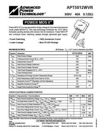
APT5012WVR 500V 40A 0.120 POWER MOS V TO-267 Power MOS V is a new generation of high voltage N-Channel enhancement mode power MOSFETs. This new technology minimizes the JFET effect, increases packing density and reduces the on-resistance. Power MOS V also achieves faster switching speeds through optimized gate layout. D Faster Switching 100% Avalanche Tested Lower
apt5012.pdf
APT5012WVR 500V 40A 0.120 POWER MOS V TO-267 Power MOS V is a new generation of high voltage N-Channel enhancement mode power MOSFETs. This new technology minimizes the JFET effect, increases packing density and reduces the on-resistance. Power MOS V also achieves faster switching speeds through optimized gate layout. D Faster Switching 100% Avalanche Tested Lower
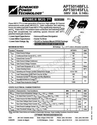
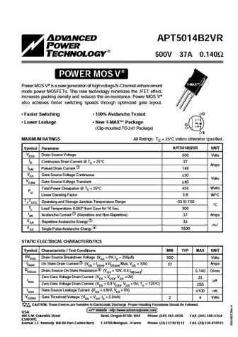
apt5014bll.pdf

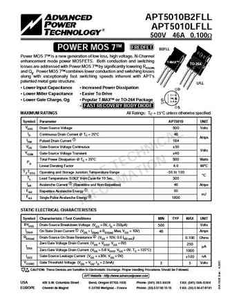
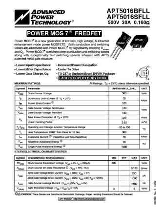
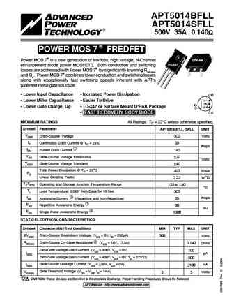
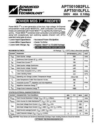
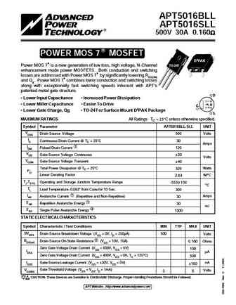
APT5014BLL APT5014SLL 500V 35A 0.140W TM BLL POWER MOS 7 Power MOS 7TM is a new generation of low loss, high voltage, N-Channel D3PAK TO-247 enhancement mode power MOSFETS. Both conduction and switching losses are addressed with Power MOS 7TM by significantly lowering RDS(ON) and Qg. Power MOS 7TM combines lower conduction and switching losses along with exceptionally fast switching
apt5018bfllg apt5018sfllg.pdf
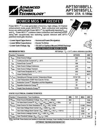
APT5018BFLL APT5018SFLL 500V 27A 0.180 BLL R POWER MOS 7 FREDFET D3PAK Power MOS 7 is a new generation of low loss, high voltage, N-Channel TO-247 enhancement mode power MOSFETS. Both conduction and switching losses are addressed with Power MOS 7 by significantly lowering RDS(ON) and Qg. Power MOS 7 combines lower conduction and switching losses SLL al
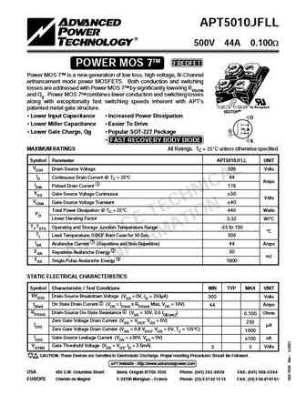
apt5010jll.pdf
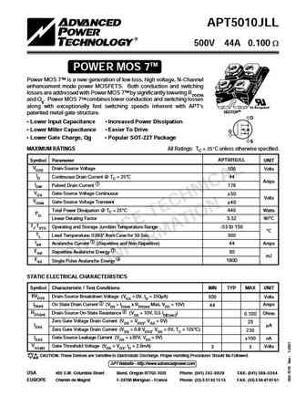
APT5010JLL 500V 44A 0.100 W TM POWER MOS 7 Power MOS 7TM is a new generation of low loss, high voltage, N-Channel enhancement mode power MOSFETS. Both conduction and switching losses are addressed with Power MOS 7TM by significantly lowering RDS(ON) and Qg. Power MOS 7TM combines lower conduction and switching losses along with exceptionally fast switching speeds inherent with APT's "
apt5010jvru3.pdf
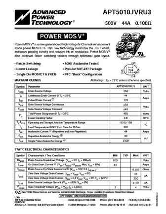
APT5010JVRU3 500V 44A 0.100 POWER MOS V Power MOS V is a new generation of high voltage N-Channel enhancement mode power MOSFETs. This new technology minimizes the JFET effect, increases packing density and reduces the on-resistance. Power MOS V also achieves faster switching speeds through optimized gate layout. "UL Recognized" ISOTOP D Faster Switching 100% Avalan
apt5010jvru2.pdf

APT5010JVRU2 500V 44A 0.100 POWER MOS V Power MOS V is a new generation of high voltage N-Channel enhancement mode power MOSFETs. This new technology minimizes the JFET effect, increases packing density and reduces the on-resistance. Power MOS V also achieves faster switching speeds through optimized gate layout. "UL Recognized" ISOTOP D Faster Switching 100% Avalan
apt5018sll.pdf
APT5018BLL APT5018SLL 500V 27A 0.180 R BLL POWER MOS 7 MOSFET D3PAK Power MOS 7 is a new generation of low loss, high voltage, N-Channel TO-247 enhancement mode power MOSFETS. Both conduction and switching losses are addressed with Power MOS 7 by significantly lowering RDS(ON) and Qg. Power MOS 7 combines lower conduction and switching losses SLL along
apt5010b2vfr.pdf
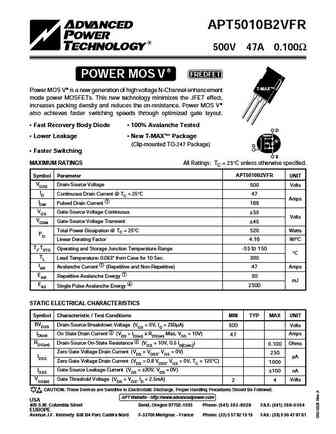
APT5010B2VFR 500V 47A 0.100 POWER MOS V FREDFET T-MAX Power MOS V is a new generation of high voltage N-Channel enhancement mode power MOSFETs. This new technology minimizes the JFET effect, increases packing density and reduces the on-resistance. Power MOS V also achieves faster switching speeds through optimized gate layout. Fast Recovery Body Diode 100% Avalanche
apt5014bfll.pdf
APT5014BFLL APT5014SFLL 500V 35A 0.140W TM BFLL FREDFET POWER MOS 7 Power MOS 7TM is a new generation of low loss, high voltage, N-Channel D3PAK TO-247 enhancement mode power MOSFETS. Both conduction and switching losses are addressed with Power MOS 7TM by significantly lowering RDS(ON) and Qg. Power MOS 7TM combines lower conduction and switching losses along with exceptionally fas
apt5015.pdf
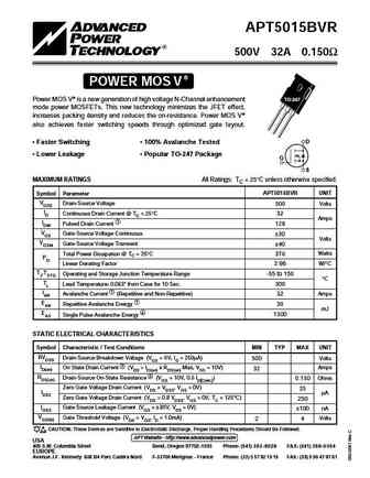
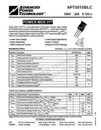
APT5015BVR 500V 32A 0.150 POWER MOS V Power MOS V is a new generation of high voltage N-Channel enhancement TO-247 mode power MOSFETs. This new technology minimizes the JFET effect, increases packing density and reduces the on-resistance. Power MOS V also achieves faster switching speeds through optimized gate layout. D Faster Switching 100% Avalanche Tested Lower
apt5010lvr.pdf
APT5010LVR 500V 47A 0.100 POWER MOS V Power MOS V is a new generation of high voltage N-Channel enhancement TO-264 mode power MOSFETs. This new technology minimizes the JFET effect, increases packing density and reduces the on-resistance. Power MOS V also achieves faster switching speeds through optimized gate layout.. Faster Switching 100% Avalanche Tested D Lower
apt5010jn.pdf
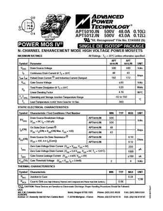
D G APT5010JN 500V 48.0A 0.10 S APT5012JN 500V 43.0A 0.12 ISOTOP "UL Recognized" File No. E145592 (S) POWER MOS IV SINGLE DIE ISOTOP PACKAGE N- CHANNEL ENHANCEMENT MODE HIGH VOLTAGE POWER MOSFETS MAXIMUM RATINGS All Ratings TC = 25 C unless otherwise specified. APT APT Symbol Parameter 5010JN 5012JN UNIT VDSS Drain-Source Voltage 500 500 Volts ID Continuous Drain Cu
apt5010b2vr.pdf

APT5010B2VR 500V 47A 0.100 POWER MOS V T-MAX Power MOS V is a new generation of high voltage N-Channel enhancement mode power MOSFETs. This new technology minimizes the JFET effect, increases packing density and reduces the on-resistance. Power MOS V also achieves faster switching speeds through optimized gate layout. Faster Switching 100% Avalanche Tested D Low
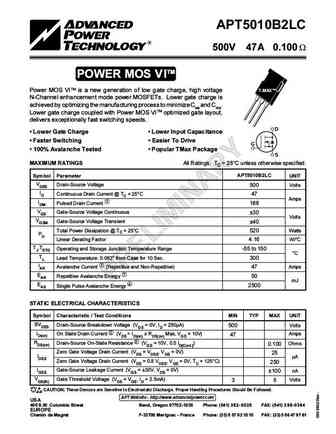
apt5010b2lc.pdf

APT5010B2LC APT5010LLC 500V 47A 0.100W B2LC TM POWER MOS VI T-MAX Power MOS VITM is a new generation of low gate charge, high voltage TO-264 N-Channel enhancement mode power MOSFETs. Lower gate charge is achieved by optimizing the manufacturing process to minimize Ciss and Crss. Lower gate charge coupled with Power MOS VITM optimized gate LLC layout, delivers exceptionally fast
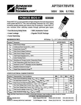
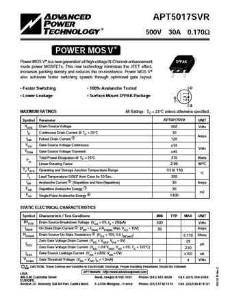
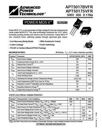
apt5017svr.pdf

APT5017SVR 500V 30A 0.170 POWER MOS V Power MOS V is a new generation of high voltage N-Channel enhancement D3PAK mode power MOSFETs. This new technology minimizes the JFET effect, increases packing density and reduces the on-resistance. Power MOS V also achieves faster switching speeds through optimized gate layout. D Faster Switching 100% Avalanche Tested Lower L
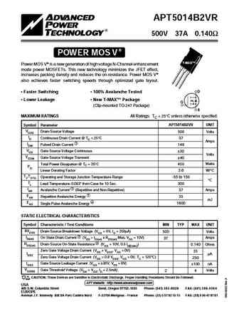
apt5014lvr.pdf

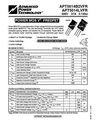
APT5014LVR 500V 37A 0.140 POWER MOS V Power MOS V is a new generation of high voltage N-Channel enhancement TO-264 mode power MOSFETs. This new technology minimizes the JFET effect, increases packing density and reduces the on-resistance. Power MOS V also achieves faster switching speeds through optimized gate layout. D Faster Switching 100% Avalanche Tested Lower
apt5017blc.pdf
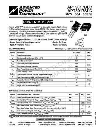
APT5017BLC APT5017SLC 500V 30A 0.170W BLC TM POWER MOS VI D3PAK Power MOS VITM is a new generation of low gate charge, high voltage TO-247 N-Channel enhancement mode power MOSFETs. Lower gate charge is achieved by optimizing the manufacturing process to minimize Ciss and Crss. Lower gate charge coupled with Power MOS VITM optimized gate layout, SLC delivers exceptionally fast switc
apt5010jlc.pdf
APT5010JLC 500V 44A 0.100 W TM POWER MOS VI Power MOS VITM is a new generation of low gate charge, high voltage N-Channel enhancement mode power MOSFETs. Lower gate charge is achieved by optimizing the manufacturing process to minimize Ciss and Crss. Lower gate charge coupled with Power MOS VITM optimized gate layout, "UL Recognized" delivers exceptionally fast switching speeds. ISOTO
apt5014b2vrg.pdf
APT5014B2VR 500V 37A 0.140 POWER MOS V T-MAX Power MOS V is a new generation of high voltage N-Channel enhancement mode power MOSFETs. This new technology minimizes the JFET effect, increases packing density and reduces the on-resistance. Power MOS V also achieves faster switching speeds through optimized gate layout. D Faster Switching 100% Avalanche Tested Lo
apt5014b2vr.pdf
APT5014B2VR 500V 37A 0.140 POWER MOS V T-MAX Power MOS V is a new generation of high voltage N-Channel enhancement mode power MOSFETs. This new technology minimizes the JFET effect, increases packing density and reduces the on-resistance. Power MOS V also achieves faster switching speeds through optimized gate layout. D Faster Switching 100% Avalanche Tested Lo
apt5010b2fll.pdf
APT5010B2FLL APT5010LFLL 500V 46A 0.100W TM FREDFET POWER MOS 7 B2FLL Power MOS 7TM is a new generation of low loss, high voltage, N-Channel enhancement mode power MOSFETS. Both conduction and switching T-MAX TO-264 losses are addressed with Power MOS 7TM by significantly lowering RDS(ON) and Qg. Power MOS 7TM combines lower conduction and switching losses along with exceptiona
apt5010jvr.pdf
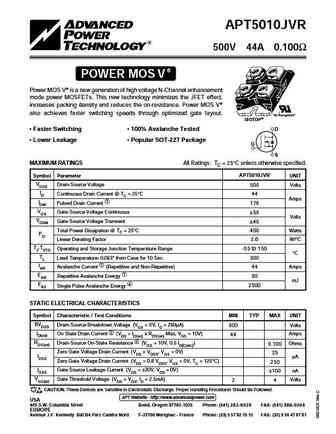
APT5010JVR 500V 44A 0.100 POWER MOS V Power MOS V is a new generation of high voltage N-Channel enhancement mode power MOSFETs. This new technology minimizes the JFET effect, increases packing density and reduces the on-resistance. Power MOS V also achieves faster switching speeds through optimized gate layout. "UL Recognized" ISOTOP Faster Switching 100% Avalanche T
apt5019hvr.pdf
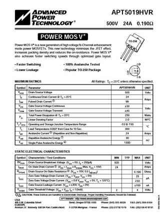
APT5019HVR 500V 24A 0.190 POWER MOS V TO-258 Power MOS V is a new generation of high voltage N-Channel enhancement mode power MOSFETs. This new technology minimizes the JFET effect, increases packing density and reduces the on-resistance. Power MOS V also achieves faster switching speeds through optimized gate layout. D Faster Switching 100% Avalanche Tested Lower
apt5010b2lc-47434900.pdf
APT5010B2LC 500V 47A 0.100 W TM POWER MOS VI Power MOS VITM is a new generation of low gate charge, high voltage T-MAX N-Channel enhancement mode power MOSFETs. Lower gate charge is achieved by optimizing the manufacturing process to minimize Ciss and C . rss Lower gate charge coupled with Power MOS VITM optimized gate layout, delivers exceptionally fast switching speeds. D L
apt5015bvr.pdf

APT5015BVR 500V 32A 0.150 POWER MOS V Power MOS V is a new generation of high voltage N-Channel enhancement TO-247 mode power MOSFETs. This new technology minimizes the JFET effect, increases packing density and reduces the on-resistance. Power MOS V also achieves faster switching speeds through optimized gate layout. D Faster Switching 100% Avalanche Tested Lower
apt5015bvfrg.pdf
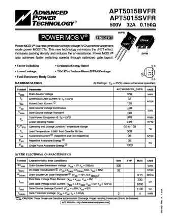
APT5015BVFR APT5015SVFR 500V 32A 0.150 BVFR POWER MOS V FREDFET D3PAK TO-247 Power MOS V is a new generation of high voltage N-Channel enhancement mode power MOSFETs. This new technology minimizes the JFET effect, increases packing density and reduces the on-resistance. Power MOS V SVFR also achieves faster switching speeds through optimized gate layout.
apt5016bfllg apt5016sfllg.pdf
APT5016BFLL APT5016SFLL 500V 30A 0.160 R POWER MOS 7 FREDFET D3PAK Power MOS 7 is a new generation of low loss, high voltage, N-Channel TO-247 enhancement mode power MOSFETS. Both conduction and switching losses are addressed with Power MOS 7 by significantly lowering RDS(ON) and Qg. Power MOS 7 combines lower conduction and switching losses along with e
apt5014.pdf

APT5014BLL APT5014SLL 500V 35A 0.140W TM BLL POWER MOS 7 Power MOS 7TM is a new generation of low loss, high voltage, N-Channel D3PAK TO-247 enhancement mode power MOSFETS. Both conduction and switching losses are addressed with Power MOS 7TM by significantly lowering RDS(ON) and Qg. Power MOS 7TM combines lower conduction and switching losses along with exceptionally fast switching
apt5014b2vfrg apt5014lvfrg.pdf
APT5014B2VFR APT5014LVFR 500V 37A 0.140 B2VFR POWER MOS V FREDFET T-MAX TO-264 Power MOS V is a new generation of high voltage N-Channel enhancement mode power MOSFETs. This new technology minimizes the JFET effect, increases packing density and reduces the on-resistance. Power MOS V also achieves faster switching speeds through optimized gate layout.
apt5010lvfr.pdf

APT5010LVFR 500V 47A 0.100 POWER MOS V FREDFET Power MOS V is a new generation of high voltage N-Channel enhancement TO-264 mode power MOSFETs. This new technology minimizes the JFET effect, increases packing density and reduces the on-resistance. Power MOS V also achieves faster switching speeds through optimized gate layout. Fast Recovery Body Diode 100% Avalanche Tes
apt5010b2llg apt5010lllg.pdf
APT5010B2LL APT5010LLL 500V 46A 0.100 B2LL R POWER MOS 7 MOSFET T-MAX TO-264 Power MOS 7 is a new generation of low loss, high voltage, N-Channel enhancement mode power MOSFETS. Both conduction and switching losses are addressed with Power MOS 7 by significantly lowering RDS(ON) and Qg. Power MOS 7 combines lower conduction and switching losses LLL
apt5016bfll.pdf

APT5016BFLL APT5016SFLL 500V 30A 0.160W TM BLL FREDFET POWER MOS 7 Power MOS 7TM is a new generation of low loss, high voltage, N-Channel D3PAK TO-247 enhancement mode power MOSFETS. Both conduction and switching losses are addressed with Power MOS 7TM by significantly lowering RDS(ON) and Qg. Power MOS 7TM combines lower conduction and switching losses along with exceptionally fast
apt5014bfllg apt5014sfllg.pdf
APT5014BFLL APT5014SFLL 500V 35A 0.140 R POWER MOS 7 FREDFET Power MOS 7 is a new generation of low loss, high voltage, N-Channel D3PAK TO-247 enhancement mode power MOSFETS. Both conduction and switching losses are addressed with Power MOS 7 by significantly lowering RDS(ON) and Qg. Power MOS 7 combines lower conduction and switching losses along with ex
apt5017bvr.pdf

APT5017BVR 500V 30A 0.170 POWER MOS V Power MOS V is a new generation of high voltage N-Channel enhancement TO-247 mode power MOSFETs. This new technology minimizes the JFET effect, increases packing density and reduces the on-resistance. Power MOS V also achieves faster switching speeds through optimized gate layout. D Faster Switching 100% Avalanche Tested Lower
apt5018bfll.pdf

APT5018BFLL APT5018SFLL 500V 27A 0.180W TM BLL FREDFET POWER MOS 7 Power MOS 7TM is a new generation of low loss, high voltage, N-Channel D3PAK TO-247 enhancement mode power MOSFETS. Both conduction and switching losses are addressed with Power MOS 7TM by significantly lowering RDS(ON) and Qg. Power MOS 7TM combines lower conduction and switching losses along with exceptionally fast
apt5014b2lc.pdf
APT5014B2LC APT5014LLC 500V 37A 0.140W B2LC TM POWER MOS VI T-MAX Power MOS VITM is a new generation of low gate charge, high voltage TO-264 N-Channel enhancement mode power MOSFETs. Lower gate charge is achieved by optimizing the manufacturing process to minimize Ciss and Crss. Lower gate charge coupled with Power MOS VITM optimized gate layout, LLC delivers exceptionally fast
apt5010b2fllg apt5010lfllg.pdf
APT5010B2FLL APT5010LFLL 500V 46A 0.100 R B2FLL POWER MOS 7 FREDFET T-MAX Power MOS 7 is a new generation of low loss, high voltage, N-Channel TO-264 enhancement mode power MOSFETS. Both conduction and switching losses are addressed with Power MOS 7 by significantly lowering RDS(ON) and Qg. Power MOS 7 combines lower conduction and switching losses a
apt5016bllg.pdf
APT5016BLL APT5016SLL 500V 30A 0.160 R POWER MOS 7 MOSFET D3PAK Power MOS 7 is a new generation of low loss, high voltage, N-Channel TO-247 enhancement mode power MOSFETS. Both conduction and switching losses are addressed with Power MOS 7 by significantly lowering RDS(ON) and Qg. Power MOS 7 combines lower conduction and switching losses along with excep
apt5010b2ll.pdf

APT5010B2LL APT5010LLL 500V 46A 0.100W B2LL TM POWER MOS 7 Power MOS 7TM is a new generation of low loss, high voltage, N-Channel T-MAX TO-264 enhancement mode power MOSFETS. Both conduction and switching losses are addressed with Power MOS 7TM by significantly lowering RDS(ON) and Qg. Power MOS 7TM combines lower conduction and switching losses along with exceptionally fast swi
apt5014bllg apt5014sllg.pdf
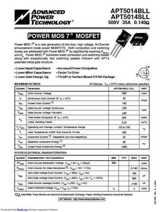
APT5014BLL APT5014SLL 500V 35A 0.140 R POWER MOS 7 MOSFET D3PAK TO-247 Power MOS 7 is a new generation of low loss, high voltage, N-Channel enhancement mode power MOSFETS. Both conduction and switching losses are addressed with Power MOS 7 by significantly lowering RDS(ON) and Qg. Power MOS 7 combines lower conduction and switching losses along with exce
apt5010b2.pdf

APT5010B2FLL APT5010LFLL 500V 46A 0.100W TM FREDFET POWER MOS 7 B2FLL Power MOS 7TM is a new generation of low loss, high voltage, N-Channel enhancement mode power MOSFETS. Both conduction and switching T-MAX TO-264 losses are addressed with Power MOS 7TM by significantly lowering RDS(ON) and Qg. Power MOS 7TM combines lower conduction and switching losses along with exceptiona
apt5016bll.pdf

APT5016BLL APT5016SLL 500V 30A 0.160W TM BLL POWER MOS 7 Power MOS 7TM is a new generation of low loss, high voltage, N-Channel D3PAK TO-247 enhancement mode power MOSFETS. Both conduction and switching losses are addressed with Power MOS 7TM by significantly lowering RDS(ON) and Qg. Power MOS 7TM combines lower conduction and switching losses along with exceptionally fast switching
apt5017bvfr.pdf
APT5017BVFR 500V 30A 0.170 POWER MOS V FREDFET Power MOS V is a new generation of high voltage N-Channel enhancement TO-247 mode power MOSFETs. This new technology minimizes the JFET effect, increases packing density and reduces the on-resistance. Power MOS V also achieves faster switching speeds through optimized gate layout. Fast Recovery Body Diode 100% Avalanche Test
apt5017.pdf
APT5017SVR 500V 30A 0.170 POWER MOS V Power MOS V is a new generation of high voltage N-Channel enhancement D3PAK mode power MOSFETs. This new technology minimizes the JFET effect, increases packing density and reduces the on-resistance. Power MOS V also achieves faster switching speeds through optimized gate layout. D Faster Switching 100% Avalanche Tested Lower L
apt5018bll.pdf

APT5018BLL APT5018SLL 500V 27A 0.180W TM BLL POWER MOS 7 Power MOS 7TM is a new generation of low loss, high voltage, N-Channel D3PAK TO-247 enhancement mode power MOSFETS. Both conduction and switching losses are addressed with Power MOS 7TM by significantly lowering RDS(ON) and Qg. Power MOS 7TM combines lower conduction and switching losses along with exceptionally fast switching
apt5010jfll.pdf
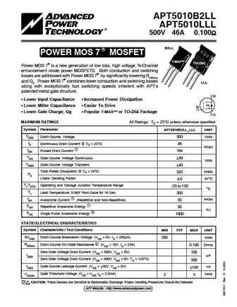
APT5010JFLL 500V 44A 0.100W TM FREDFET POWER MOS 7 Power MOS 7TM is a new generation of low loss, high voltage, N-Channel enhancement mode power MOSFETS. Both conduction and switching losses are addressed with Power MOS 7TM by significantly lowering RDS(ON) and Qg. Power MOS 7TM combines lower conduction and switching losses along with exceptionally fast switching speeds inherent with
apt5017svfrg.pdf
APT5017BVFR APT5017SVFR 500V 30A 0.170 POWER MOS V FREDFET TO-247 D3PAK Power MOS V is a new generation of high voltage N-Channel enhancement mode power MOSFETs. This new technology minimizes the JFET effect, increases packing density and reduces the on-resistance. Power MOS V also achieves faster switching speeds through optimized gate layout. D Fast
apt5010jvfr.pdf
APT5010JVFR 500V 44A 0.100 POWER MOS V FREDFET Power MOS V is a new generation of high voltage N-Channel enhancement mode power MOSFETs. This new technology minimizes the JFET effect, increases packing density and reduces the on-resistance. Power MOS V also achieves faster switching speeds through optimized gate layout. "UL Recognized" ISOTOP Fast Recovery Body Diode
apt5016.pdf

APT5016BFLL APT5016SFLL 500V 30A 0.160W TM BLL FREDFET POWER MOS 7 Power MOS 7TM is a new generation of low loss, high voltage, N-Channel D3PAK TO-247 enhancement mode power MOSFETS. Both conduction and switching losses are addressed with Power MOS 7TM by significantly lowering RDS(ON) and Qg. Power MOS 7TM combines lower conduction and switching losses along with exceptionally fast
apt5015blc.pdf
APT5015BLC 500V 32A 0.150 W TM POWER MOS VI Power MOS VITM is a new generation of low gate charge, high voltage TO-247 N-Channel enhancement mode power MOSFETs. Lower gate charge is achieved by optimizing the manufacturing process to minimize Ciss and Crss. Lower gate charge coupled with Power MOS VITM optimized gate layout, delivers exceptionally fast switching speeds. D Lower G
apt5014bll.pdf

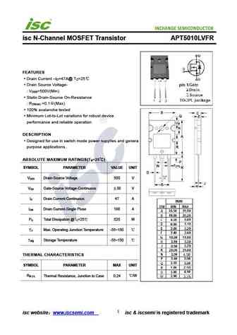
isc N-Channel MOSFET Transistor APT5014BLL FEATURES Drain Current I =35A@ T =25 D C Drain Source Voltage- V =500V(Min) DSS Static Drain-Source On-Resistance R =0.14 (Max) DS(on) 100% avalanche tested Minimum Lot-to-Lot variations for robust device performance and reliable operation DESCRIPTION Designed for use in switch mode power supplies and general purpo
apt5014bfll.pdf

isc N-Channel MOSFET Transistor APT5014BFLL FEATURES Drain Current I =35A@ T =25 D C Drain Source Voltage- V =500V(Min) DSS Static Drain-Source On-Resistance R =0.14 (Max) DS(on) 100% avalanche tested Minimum Lot-to-Lot variations for robust device performance and reliable operation DESCRIPTION Designed for use in switch mode power supplies and general purp
apt5015bvfr.pdf

isc N-Channel MOSFET Transistor APT5015BVFR FEATURES Drain Current I =32A@ T =25 D C Drain Source Voltage- V =500V(Min) DSS Static Drain-Source On-Resistance R =0.15 (Max) DS(on) 100% avalanche tested Minimum Lot-to-Lot variations for robust device performance and reliable operation DESCRIPTION Designed for use in switch mode power supplies and general purp
apt5010lfll.pdf
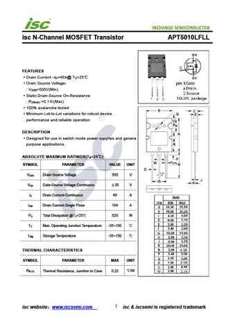
isc N-Channel MOSFET Transistor APT5010LFLL FEATURES Drain Current I =46A@ T =25 D C Drain Source Voltage- V =500V(Min) DSS Static Drain-Source On-Resistance R =0.1 (Max) DS(on) 100% avalanche tested Minimum Lot-to-Lot variations for robust device performance and reliable operation DESCRIPTION Designed for use in switch mode power supplies and general purpo
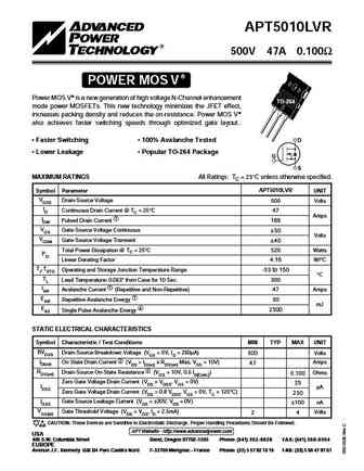
apt5010lvr.pdf

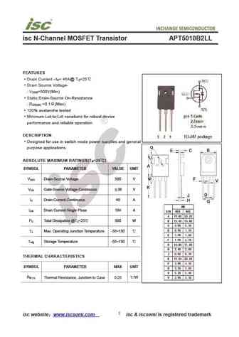
isc N-Channel MOSFET Transistor APT5010LVR FEATURES Drain Current I =47A@ T =25 D C Drain Source Voltage- V =500V(Min) DSS Static Drain-Source On-Resistance R =0.1 (Max) DS(on) 100% avalanche tested Minimum Lot-to-Lot variations for robust device performance and reliable operation DESCRIPTION Designed for use in switch mode power supplies and general purpos
apt5010b2fll.pdf

isc N-Channel MOSFET Transistor APT5010B2FLL FEATURES Drain Current I = 46A@ T =25 D C Drain Source Voltage- V =500V(Min) DSS Static Drain-Source On-Resistance R =0.1 (Max) DS(on) 100% avalanche tested Minimum Lot-to-Lot variations for robust device performance and reliable operation DESCRIPTION Designed for use in switch mode power supplies and general pur
apt5015bvr.pdf
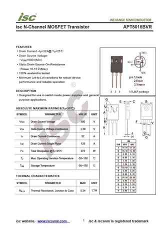
isc N-Channel MOSFET Transistor APT5015BVR FEATURES Drain Current I =32A@ T =25 D C Drain Source Voltage- V =500V(Min) DSS Static Drain-Source On-Resistance R =0.15 (Max) DS(on) 100% avalanche tested Minimum Lot-to-Lot variations for robust device performance and reliable operation DESCRIPTION Designed for use in switch mode power supplies and general purpo
apt5010lvfr.pdf
isc N-Channel MOSFET Transistor APT5010LVFR FEATURES Drain Current I =47A@ T =25 D C Drain Source Voltage- V =500V(Min) DSS Static Drain-Source On-Resistance R =0.1 (Max) DS(on) 100% avalanche tested Minimum Lot-to-Lot variations for robust device performance and reliable operation DESCRIPTION Designed for use in switch mode power supplies and general purpo
apt5016bfll.pdf

isc N-Channel MOSFET Transistor APT5016BFLL FEATURES Drain Current I =30A@ T =25 D C Drain Source Voltage- V =500V(Min) DSS Static Drain-Source On-Resistance R =0.16 (Max) DS(on) 100% avalanche tested Minimum Lot-to-Lot variations for robust device performance and reliable operation DESCRIPTION Designed for use in switch mode power supplies and general purp
apt5017bvr.pdf

isc N-Channel MOSFET Transistor APT5017BVR FEATURES Drain Current I =30A@ T =25 D C Drain Source Voltage- V =500V(Min) DSS Static Drain-Source On-Resistance R =0.17 (Max) DS(on) 100% avalanche tested Minimum Lot-to-Lot variations for robust device performance and reliable operation DESCRIPTION Designed for use in switch mode power supplies and general purpo
apt5018bfll.pdf

isc N-Channel MOSFET Transistor APT5018BFLL FEATURES Drain Current I =27A@ T =25 D C Drain Source Voltage- V =500V(Min) DSS Static Drain-Source On-Resistance R =0.18 (Max) DS(on) 100% avalanche tested Minimum Lot-to-Lot variations for robust device performance and reliable operation DESCRIPTION Designed for use in switch mode power supplies and general purp
apt5010b2ll.pdf
isc N-Channel MOSFET Transistor APT5010B2LL FEATURES Drain Current I = 46A@ T =25 D C Drain Source Voltage- V =500V(Min) DSS Static Drain-Source On-Resistance R =0.1 (Max) DS(on) 100% avalanche tested Minimum Lot-to-Lot variations for robust device performance and reliable operation DESCRIPTION Designed for use in switch mode power supplies and general purp
apt5016bll.pdf

isc N-Channel MOSFET Transistor APT5016BLL FEATURES Drain Current I =30A@ T =25 D C Drain Source Voltage- V =500V(Min) DSS Static Drain-Source On-Resistance R =0.16 (Max) DS(on) 100% avalanche tested Minimum Lot-to-Lot variations for robust device performance and reliable operation DESCRIPTION Designed for use in switch mode power supplies and general purpo
apt5017bvfr.pdf

isc N-Channel MOSFET Transistor APT5017BVFR FEATURES Drain Current I =30A@ T =25 D C Drain Source Voltage- V =500V(Min) DSS Static Drain-Source On-Resistance R =0.17 (Max) DS(on) 100% avalanche tested Minimum Lot-to-Lot variations for robust device performance and reliable operation DESCRIPTION Designed for use in switch mode power supplies and general purp
apt5018bll.pdf

isc N-Channel MOSFET Transistor APT5018BLL FEATURES Drain Current I =27A@ T =25 D C Drain Source Voltage- V =500V(Min) DSS Static Drain-Source On-Resistance R =0.18 (Max) DS(on) 100% avalanche tested Minimum Lot-to-Lot variations for robust device performance and reliable operation DESCRIPTION Designed for use in switch mode power supplies and general purpo
apt5010lll.pdf

isc N-Channel MOSFET Transistor APT5010LLL FEATURES Drain Current I = 46A@ T =25 D C Drain Source Voltage- V =500V(Min) DSS Static Drain-Source On-Resistance R =0.1 (Max) DS(on) 100% avalanche tested Minimum Lot-to-Lot variations for robust device performance and reliable operation DESCRIPTION Designed for use in switch mode power supplies and general purpo
Другие MOSFET... APT48M80L , APT4F120K , APT4F120S , APT4M120K , APT5010B2FLLG , APT5010B2LLG , APT5010LFLLG , APT5010LLLG , 2SK3568 , APT5014B2VFRG , APT5014B2VRG , APT5014BFLLG , APT5014BLLG , APT5014LVFRG , APT5014SFLLG , APT5014SLLG , APT5015BVFRG .
History: FDB0300N1007L | 2SJ374 | ME8205E-G
History: FDB0300N1007L | 2SJ374 | ME8205E-G
🌐 : EN ES РУ

Список транзисторов
Обновления
MOSFET: AUB062N08BG | AUB060N08AG | AUB056N10 | AUB056N08BGL | AUB050N085 | AUB050N055 | AUB045N12 | AUB045N10BT | AUB039N10 | AUB034N10 | AUB033N08BG | AUB026N085 | AUA062N08BG | AUA060N08AG | AUA056N08BGL | AUA039N10
Popular searches
2sc461 | hy1906 | 2sc2238 | 2sc458 transistor | b649a transistor | 2sa606 | 2n3644 | 2sc2240bl