APT6070AN datasheet, аналоги, основные параметры
Наименование производителя: APT6070AN 📄📄
Тип транзистора: MOFETS
Полярность: N
Предельные значения
Pd ⓘ - Максимальная рассеиваемая мощность: 198 W
|Vds|ⓘ - Максимально допустимое напряжение сток-исток: 600 V
|Vgs|ⓘ - Максимально допустимое напряжение затвор-исток: 30 V
|Id| ⓘ - Максимально допустимый постоянный ток стока: 10.5 A
Tj ⓘ - Максимальная температура канала: 150 °C
Электрические характеристики
tr ⓘ - Время нарастания: 18 ns
Cossⓘ - Выходная емкость: 280 pf
RDSonⓘ - Сопротивление сток-исток открытого транзистора: 0.7 Ohm
Тип корпуса: TO-3
📄📄 Копировать
Аналог (замена) для APT6070AN
- подборⓘ MOSFET транзистора по параметрам
APT6070AN даташит
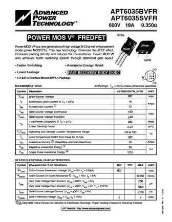
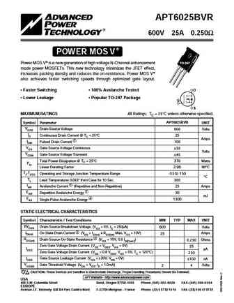
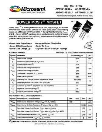
apt6045bvr.pdf

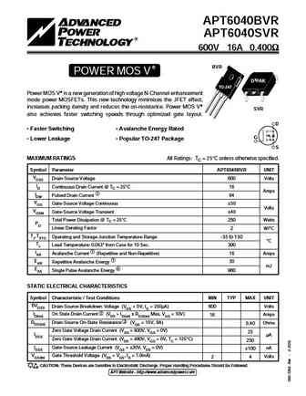
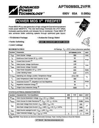
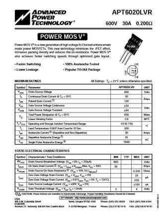
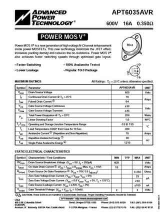
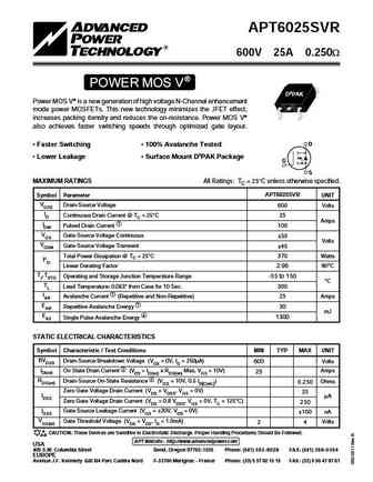
APT6045BVR 600V 15A 0.450 POWER MOS V Power MOS V is a new generation of high voltage N-Channel enhancement TO-247 mode power MOSFETs. This new technology minimizes the JFET effect, increases packing density and reduces the on-resistance. Power MOS V also achieves faster switching speeds through optimized gate layout. Faster Switching 100% Avalanche Tested D Lower L
apt60m80jvr.pdf
APT60M80JVR 600V 55A 0.080 POWER MOS V Power MOS V is a new generation of high voltage N-Channel enhancement mode power MOSFETs. This new technology minimizes the JFET effect, increases packing density and reduces the on-resistance. Power MOS V also achieves faster switching speeds through optimized gate layout. "UL Recognized" ISOTOP Popular SOT-227
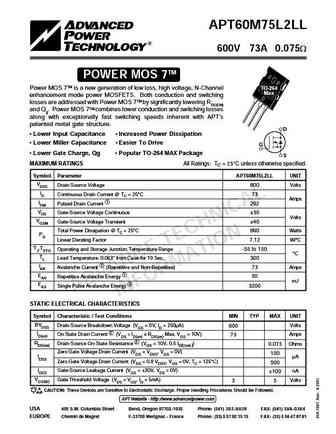
apt60m75l2llg.pdf
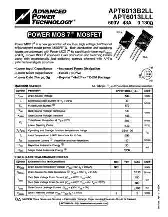
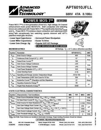
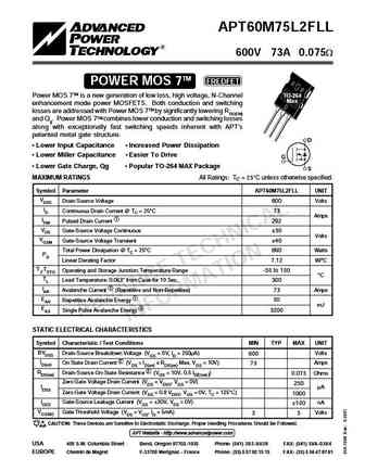
APT60M75L2LL 600V 73A 0.075 R POWER MOS 7 MOSFET TO-264 Max Power MOS 7 is a new generation of low loss, high voltage, N-Channel enhancement mode power MOSFETS. Both conduction and switching losses are addressed with Power MOS 7 by significantly lowering RDS(ON) and Qg. Power MOS 7 combines lower conduction and switching losses along with exceptionally fa
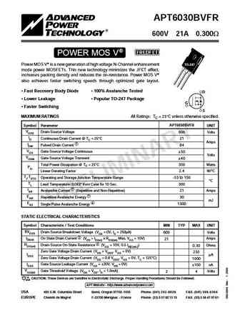
apt6030bvr.pdf

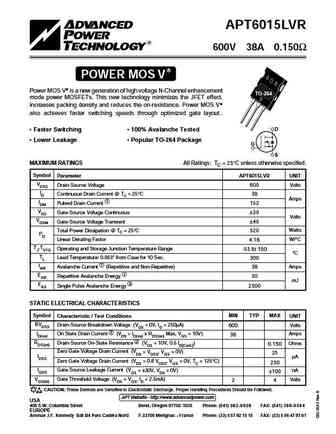
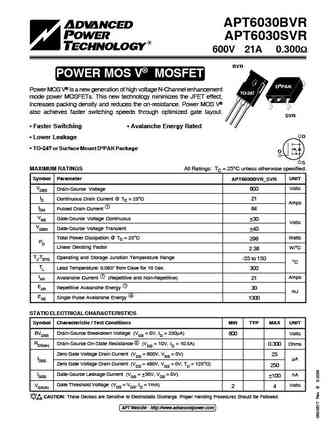
APT6030BVR 600V 21A 0.300 POWER MOS V Power MOS V is a new generation of high voltage N-Channel enhancement TO-247 mode power MOSFETs. This new technology minimizes the JFET effect, increases packing density and reduces the on-resistance. Power MOS V also achieves faster switching speeds through optimized gate layout. Faster Switching 100% Avalanche Tested D Lower L
apt6017b2ll.pdf

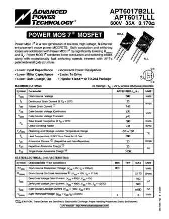
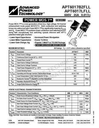
APT6017B2LL APT6017LLL 600V 35A 0.170W B2LL TM POWER MOS 7 Power MOS 7TM is a new generation of low loss, high voltage, N-Channel T-MAX TO-264 enhancement mode power MOSFETS. Both conduction and switching losses are addressed with Power MOS 7TM by significantly lowering RDS(ON) and Qg. Power MOS 7TM combines lower conduction and switching losses along with exceptionally fast swi
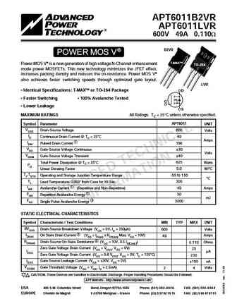
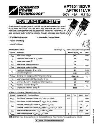
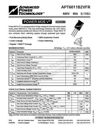
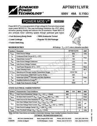
apt6011b2vfrg apt6011lvfrg.pdf
APT6011B2VFR APT6011LVFR 600V 49A 0.110 B2VFR POWER MOS V FREDFET T-MAX TO-264 Power MOS V is a new generation of high voltage N-Channel enhancement mode power MOSFETs. This new technology minimizes the JFET effect, increases packing density and reduces the on-resistance. Power MOS V also achieves faster switching speeds through optimized gate layout.
apt6013b2fll.pdf

APT6013B2FLL APT6013LFLL 600V 43A 0.130W TM FREDFET POWER MOS 7 B2FLL Power MOS 7TM is a new generation of low loss, high voltage, N-Channel enhancement mode power MOSFETS. Both conduction and switching T-MAX TO-264 losses are addressed with Power MOS 7TM by significantly lowering RDS(ON) and Qg. Power MOS 7TM combines lower conduction and switching losses along with exceptiona
apt60m75l2ll.pdf
APT60M75L2LL 600V 73A 0.075W TM POWER MOS 7 Power MOS 7TM is a new generation of low loss, high voltage, N-Channel TO-264 Max enhancement mode power MOSFETS. Both conduction and switching losses are addressed with Power MOS 7TM by significantly lowering RDS(ON) and Qg. Power MOS 7TM combines lower conduction and switching losses along with exceptionally fast switching speeds inherent
apt6015lvfr.pdf

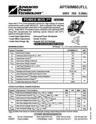
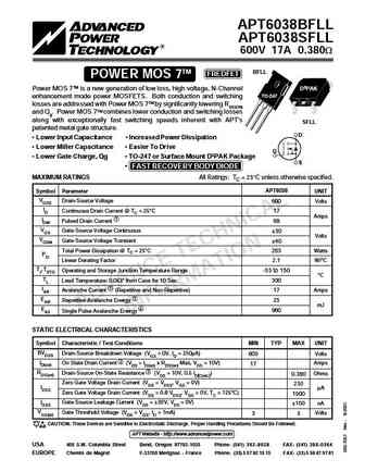
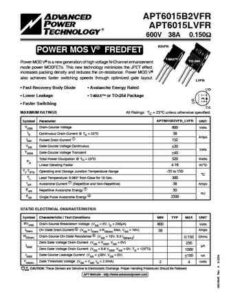
APT6015LVFR 600V 38A 0.150W POWER MOS V FREDFET Power MOS V is a new generation of high voltage N-Channel enhancement TO-264 mode power MOSFETs. This new technology minimizes the JFET effect, increases packing density and reduces the on-resistance. Power MOS V also achieves faster switching speeds through optimized gate layout. Fast Recovery Body Diode 100% Avalanche Teste
apt6029bfllg apt6029sfllg.pdf
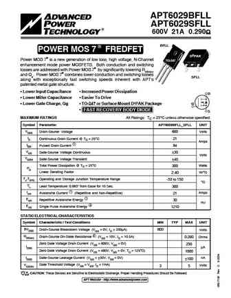
APT6029BFLL APT6029SFLL 600V 21A 0.290 BFLL R POWER MOS 7 FREDFET D3PAK Power MOS 7 is a new generation of low loss, high voltage, N-Channel TO-247 enhancement mode power MOSFETS. Both conduction and switching losses are addressed with Power MOS 7 by significantly lowering RDS(ON) and Qg. Power MOS 7 combines lower conduction and switching losses SFLL
apt6015b2vr.pdf

APT6015B2VR 600V 38A 0.150 POWER MOS V T-MAX Power MOS V is a new generation of high voltage N-Channel enhancement mode power MOSFETs. This new technology minimizes the JFET effect, increases packing density and reduces the on-resistance. Power MOS V also achieves faster switching speeds through optimized gate layout. Faster Switching 100% Avalanche Tested D Low
apt60m75l2fllg.pdf
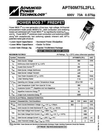
APT60M75L2FLL 600V 73A 0.075 R POWER MOS 7 FREDFET TO-264 Power MOS 7 is a new generation of low loss, high voltage, N-Channel Max enhancement mode power MOSFETS. Both conduction and switching losses are addressed with Power MOS 7 by significantly lowering RDS(ON) and Qg. Power MOS 7 combines lower conduction and switching losses along with exceptionally
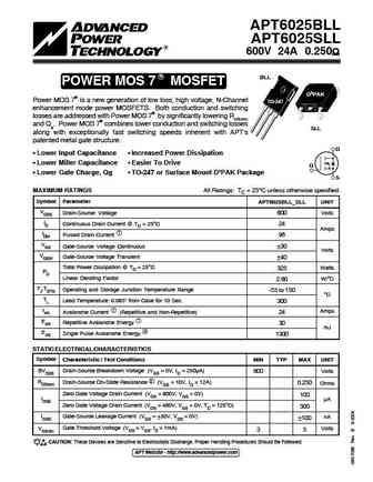
apt6035bn.pdf
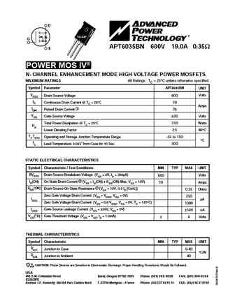
D TO-247 G APT6035BN 600V 19.0A 0.35 S POWER MOS IV N- CHANNEL ENHANCEMENT MODE HIGH VOLTAGE POWER MOSFETS MAXIMUM RATINGS All Ratings TC = 25 C unless otherwise specified. Symbol Parameter APT6035BN UNIT VDSS Drain-Source Voltage 600 Volts ID Continuous Drain Current @ TC = 25 C 19 Amps IDM Pulsed Drain Current 1 76 VGS Gate-Source Voltage 30 Volts Total Power Dissi
apt6045bn.pdf

D TO-247 G APT6040BN 600V 18.0A 0.40 S APT6045BN 600V 17.0A 0.45 POWER MOS IV N- CHANNEL ENHANCEMENT MODE HIGH VOLTAGE POWER MOSFETS MAXIMUM RATINGS All Ratings TC = 25 C unless otherwise specified. APT APT Symbol Parameter 6040BN 6045BN UNIT VDSS Drain-Source Voltage 600 600 Volts ID Continuous Drain Current @ TC = 25 C 18 17 Amps IDM Pulsed Drain Current 1 72 68 V
apt6025bfllg apt6025sfllg.pdf

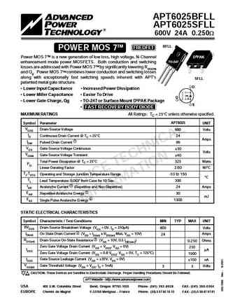
APT6025BFLL APT6025SFLL 600V 24A 0.250 BFLL R POWER MOS 7 FREDFET D3PAK Power MOS 7 is a new generation of low loss, high voltage, N-Channel TO-247 enhancement mode power MOSFETS. Both conduction and switching losses are addressed with Power MOS 7 by significantly lowering RDS(ON) and Qg. Power MOS 7 combines lower conduction and switching losses SFLL
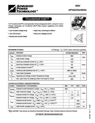
apt60gt60jr.pdf
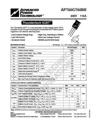
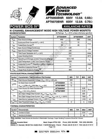
APT60GT60JR 600V 90A Thunderbolt IGBT The Thunderbolt IGBT is a new generation of high voltage power IGBTs. Using Non-Punch Through Technology the Thunderbolt IGBT offers superior ruggedness and ultrafast switching speed. "UL Recognized" ISOTOP Low Forward Voltage Drop High Freq. Switching to 150KHz C Low Tail Current Ultra Low Leakage Current Avalanche
apt60m80l2vrg.pdf
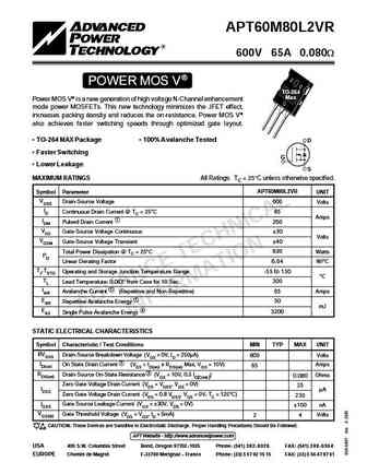
APT60M80L2VR 600V 65A 0.080 POWER MOS V MOSFET L2VR TO-264 Max Power MOS V is a new generation of high voltage N-Channel enhancement mode power MOSFETs. This new technology minimizes the JFET effect, increases packing density and reduces the on-resistance. Power MOS V also achieves faster switching speeds through optimized gate layout. TO-264 MAX Pack
apt60m75jvfr.pdf
APT60M75JVFR 600V 62A 0.075 POWER MOS V FREDFET Power MOS V is a new generation of high voltage N-Channel enhancement mode power MOSFETs. This new technology minimizes the JFET effect, increases packing density and reduces the on-resistance. Power MOS V "UL Recognized" also achieves faster switching speeds through optimized gate layout. ISOTOP Faster
apt6017b2fllg apt6017lfllg.pdf
APT6017B2FLL APT6017LFLL 600V 35A 0.170 B2FLL R POWER MOS 7 FREDFET T-MAX TO-264 Power MOS 7 is a new generation of low loss, high voltage, N-Channel enhancement mode power MOSFETS. Both conduction and switching losses are addressed with Power MOS 7 by significantly lowering RDS(ON) and Qg. Power MOS 7 combines lower conduction and switching losses L
apt6011lvr.pdf
APT6011B2VR APT6011LVR 600V 49A 0.110W B2VR POWER MOS V T-MAX Power MOS V is a new generation of high voltage N-Channel enhancement TO-264 mode power MOSFETs. This new technology minimizes the JFET effect, increases packing density and reduces the on-resistance. Power MOS V also achieves faster switching speeds through optimized gate layout. LVR Identical Specifications
apt60gf60ju2.pdf
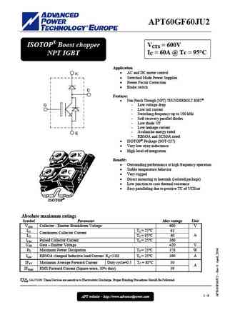
APT60GF60JU2 ISOTOP Boost chopper VCES = 600V IC = 60A @ Tc = 95 C NPT IGBT Application AC and DC motor control K Switched Mode Power Supplies Power Factor Correction Brake switch C Features Non Punch Through (NPT) THUNDERBOLT IGBT G - Low voltage drop - Low tail current - Switching frequency up to 100 kHz - Soft recovery parallel diodes - L
apt6025bll.pdf

APT6025BLL APT6025SLL 600V 24A 0.250W TM BLL POWER MOS 7 Power MOS 7TM is a new generation of low loss, high voltage, N-Channel D3PAK TO-247 enhancement mode power MOSFETS. Both conduction and switching losses are addressed with Power MOS 7TM by significantly lowering RDS(ON) and Qg. Power MOS 7TM combines lower conduction and switching losses along with exceptionally fast switching
apt6035bvr.pdf

APT6035BVR 600V 18A 0.350 POWER MOS V Power MOS V is a new generation of high voltage N-Channel enhancement TO-247 mode power MOSFETs. This new technology minimizes the JFET effect, increases packing density and reduces the on-resistance. Power MOS V also achieves faster switching speeds through optimized gate layout. Faster Switching 100% Avalanche Tested D Lower L
apt6040bn.pdf

D TO-247 G APT6040BN 600V 18.0A 0.40 S APT6045BN 600V 17.0A 0.45 POWER MOS IV N- CHANNEL ENHANCEMENT MODE HIGH VOLTAGE POWER MOSFETS MAXIMUM RATINGS All Ratings TC = 25 C unless otherwise specified. APT APT Symbol Parameter 6040BN 6045BN UNIT VDSS Drain-Source Voltage 600 600 Volts ID Continuous Drain Current @ TC = 25 C 18 17 Amps IDM Pulsed Drain Current 1 72 68 V
apt60gf120jrd.pdf
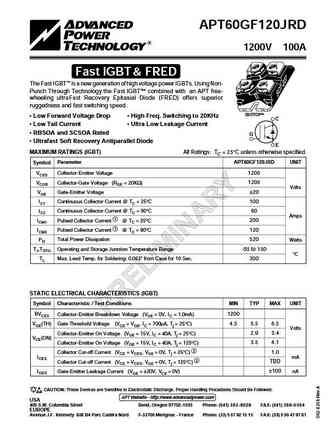
APT60GF120JRD 1200V 100A Fast IGBT & FRED The Fast IGBT is a new generation of high voltage power IGBTs. Using Non- Punch Through Technology the Fast IGBT combined with an APT free- wheeling ultraFast Recovery Epitaxial Diode (FRED) offers superior ruggedness and fast switching speed. "UL Recognized" ISOTOP Low Forward Voltage Drop High Freq. Switching to 20KHz C
apt6025bvfrg apt6025svfrg.pdf
APT6025BVFR APT6025SVFR 600V 25A 0.250 POWER MOS V FREDFET D3PAK TO-247 Power MOS V is a new generation of high voltage N-Channel enhancement mode power MOSFETs. This new technology minimizes the JFET effect, increases packing density and reduces the on-resistance. Power MOS V also achieves faster switching speeds through optimized gate layout. Fast Re
apt6035.pdf

APT6035AVR 600V 16A 0.350 POWER MOS V TO-3 Power MOS V is a new generation of high voltage N-Channel enhancement mode power MOSFETs. This new technology minimizes the JFET effect, increases packing density and reduces the on-resistance. Power MOS V also achieves faster switching speeds through optimized gate layout. D Faster Switching 100% Avalanche Tested Lower L
apt6011b2vr.pdf
APT6011B2VR APT6011LVR 600V 49A 0.110 B2VR POWER MOS V MOSFET T-MAX TO-264 Power MOS V is a new generation of high voltage N-Channel enhancement mode power MOSFETs. This new technology minimizes the JFET effect, increases packing density and reduces the on-resistance. Power MOS V also achieves faster switching speeds through optimized gate layout. LVR
apt6025bllg.pdf
APT6025BLL APT6025SLL 600V 24A 0.250 R BLL POWER MOS 7 MOSFET D3PAK Power MOS 7 is a new generation of low loss, high voltage, N-Channel TO-247 enhancement mode power MOSFETS. Both conduction and switching losses are addressed with Power MOS 7 by significantly lowering RDS(ON) and Qg. Power MOS 7 combines lower conduction and switching losses SLL along
apt6013jvr.pdf

APT6013JVR 600V 40A 0.130 POWER MOS V Power MOS V is a new generation of high voltage N-Channel enhancement mode power MOSFETs. This new technology minimizes the JFET effect, increases packing density and reduces the on-resistance. Power MOS V also achieves faster switching speeds through optimized gate layout. "UL Recognized" ISOTOP D Faster Switching 100% Avalanch
apt60gf120jrdq3.pdf
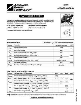
TYPICAL PERFORMANCE CURVES APT60GF120JRDQ3 1200V APT60GF120JRDQ3 FAST IGBT & FRED The Fast IGBT is a new generation of high voltage power IGBTs. Using Non-Punch through technology, the Fast IGBT combined with an APT free wheeling Ultra Fast Recovery Epi- taxial Diode (FRED) offers superior ruggedness and fast switching speed. "UL Recognized" ISOTOP file # E145592 Low Forwa
apt6033bn.pdf
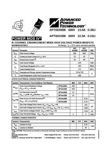
D TO-247 G APT6030BN 600V 23.0A 0.30 S APT6033BN 600V 22.0A 0.33 POWER MOS IV N- CHANNEL ENHANCEMENT MODE HIGH VOLTAGE POWER MOSFETS MAXIMUM RATINGS All Ratings TC = 25 C unless otherwise specified. APT APT Symbol Parameter 6030BN 6033BN UNIT VDSS Drain-Source Voltage 600 600 Volts ID Continuous Drain Current @ TC = 25 C 23 22 Amps IDM Pulsed Drain Current 1 92 88 V
apt6030svfr.pdf

APT6030BVFR APT6030SVFR 600V 21A 0.300 BVFR POWER MOS V FREDFET D3PAK Power MOS V is a new generation of high voltage N-Channel enhancement TO-247 mode power MOSFETs. This new technology minimizes the JFET effect, increases packing density and reduces the on-resistance. Power MOS V also achieves faster switching speeds through optimized gate layout. SVFR
apt6037hvr.pdf

APT6037HVR 600V 15.5A 0.370 POWER MOS V TO-258 Power MOS V is a new generation of high voltage N-Channel enhancement mode power MOSFETs. This new technology minimizes the JFET effect, increases packing density and reduces the on-resistance. Power MOS V also achieves faster switching speeds through optimized gate layout. Faster Switching 100% Avalanche Tested D Lowe
apt6040bvfr.pdf

APT6040BVFR APT6040SVFR 600V 16A 0.400 BVFR POWER MOS V FREDFET D3PAK Power MOS V is a new generation of high voltage N-Channel enhancement TO-247 mode power MOSFETs. This new technology minimizes the JFET effect, increases packing density and reduces the on-resistance. Power MOS V also achieves faster switching speeds through optimized gate layout. SVFR
apt6013b2ll.pdf

APT6013B2LL APT6013LLL 600V 43A 0.130W B2LL TM POWER MOS 7 Power MOS 7TM is a new generation of low loss, high voltage, N-Channel T-MAX TO-264 enhancement mode power MOSFETS. Both conduction and switching losses are addressed with Power MOS 7TM by significantly lowering RDS(ON) and Qg. Power MOS 7TM combines lower conduction and switching losses along with exceptionally fast swi
apt6013b2llg apt6013lllg.pdf
APT6013B2LL APT6013LLL 600V 43A 0.130 B2LL R POWER MOS 7 MOSFET T-MAX TO-264 Power MOS 7 is a new generation of low loss, high voltage, N-Channel enhancement mode power MOSFETS. Both conduction and switching losses are addressed with Power MOS 7 by significantly lowering RDS(ON) and Qg. Power MOS 7 combines lower conduction and switching losses LLL
apt6025bvrg.pdf

APT6025BVR 600V 25A 0.250 POWER MOS V Power MOS V is a new generation of high voltage N-Channel enhancement TO-247 mode power MOSFETs. This new technology minimizes the JFET effect, increases packing density and reduces the on-resistance. Power MOS V also achieves faster switching speeds through optimized gate layout. Faster Switching 100% Avalanche Tested D Lower L
apt6032avr.pdf
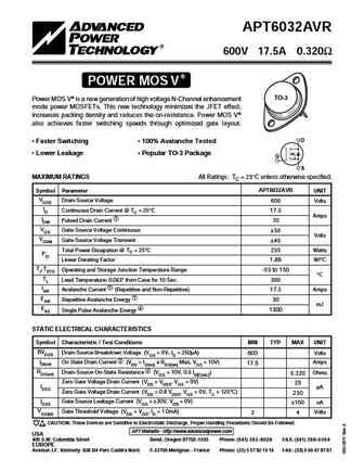
APT6032AVR 600V 17.5A 0.320 POWER MOS V TO-3 Power MOS V is a new generation of high voltage N-Channel enhancement mode power MOSFETs. This new technology minimizes the JFET effect, increases packing density and reduces the on-resistance. Power MOS V also achieves faster switching speeds through optimized gate layout. D Faster Switching 100% Avalanche Tested Lower
apt60gf60ju3.pdf
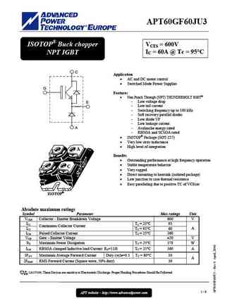
APT60GF60JU3 ISOTOP Buck chopper VCES = 600V IC = 60A @ Tc = 95 C NPT IGBT C Application AC and DC motor control Switched Mode Power Supplies G Features Non Punch Through (NPT) THUNDERBOLT IGBT - Low voltage drop E - Low tail current - Switching frequency up to 100 kHz - Soft recovery parallel diodes - Low diode VF - Low leakage current A - Avala
apt6015jvr.pdf
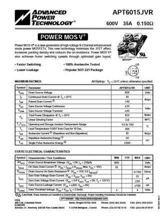
APT6015JVR 600V 35A 0.150 POWER MOS V Power MOS V is a new generation of high voltage N-Channel enhancement mode power MOSFETs. This new technology minimizes the JFET effect, increases packing density and reduces the on-resistance. Power MOS V also achieves faster switching speeds through optimized gate layout. "UL Recognized" ISOTOP Faster Switching 100% Avalanche T
apt6017wvr.pdf
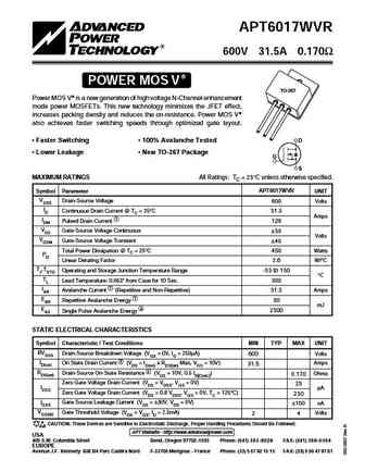
APT6017WVR 600V 31.5A 0.170 POWER MOS V TO-267 Power MOS V is a new generation of high voltage N-Channel enhancement mode power MOSFETs. This new technology minimizes the JFET effect, increases packing density and reduces the on-resistance. Power MOS V also achieves faster switching speeds through optimized gate layout. Faster Switching 100% Avalanche Tested D Lowe
apt60gt60jrdq3.pdf
TYPICAL PERFORMANCE CURVES APT60GT60JRDQ3 600V APT60GT60JRDQ3 Thunderbolt IGBT The Thunderblot IGBT is a new generation of high voltage power IGBTs. Using Non- Punch Through Technology, the Thunderblot IGBT offers superior ruggedness and ultrafast switching speed. "UL Recognized" ISOTOP file # E145592 Low Forward Voltage Drop High Freq. Switching to 100KHz
apt6030bvfr.pdf
APT6030BVFR 600V 21A 0.300W POWER MOS V FREDFET Power MOS V is a new generation of high voltage N-Channel enhancement TO-247 mode power MOSFETs. This new technology minimizes the JFET effect, increases packing density and reduces the on-resistance. Power MOS V also achieves faster switching speeds through optimized gate layout. Fast Recovery Body Diode 100% Avalanche Tested
apt60m60jfll.pdf
APT60M60JFLL 600V 70A 0.060W TM FREDFET POWER MOS 7 Power MOS 7TM is a new generation of low loss, high voltage, N-Channel enhancement mode power MOSFETS. Both conduction and switching losses are addressed with Power MOS 7TM by significantly lowering RDS(ON) and Qg. Power MOS 7TM combines lower conduction and switching losses along with exceptionally fast switching speeds inherent wit
apt6015lvr.pdf
APT6015LVR 600V 38A 0.150 POWER MOS V Power MOS V is a new generation of high voltage N-Channel enhancement TO-264 mode power MOSFETs. This new technology minimizes the JFET effect, increases packing density and reduces the on-resistance. Power MOS V also achieves faster switching speeds through optimized gate layout.. D Faster Switching 100% Avalanche Tested Lowe
apt6038bfll.pdf
APT6038BFLL APT6038SFLL 600V 17A 0.380W TM BFLL FREDFET POWER MOS 7 Power MOS 7TM is a new generation of low loss, high voltage, N-Channel D3PAK TO-247 enhancement mode power MOSFETS. Both conduction and switching losses are addressed with Power MOS 7TM by significantly lowering RDS(ON) and Qg. Power MOS 7TM combines lower conduction and switching losses along with exceptionally fas
apt6030svr.pdf
APT6030BVR APT6030SVR 600V 21A 0.300 BVR POWER MOS V MOSFET D3PAK Power MOS V is a new generation of high voltage N-Channel enhancement TO-247 mode power MOSFETs. This new technology minimizes the JFET effect, increases packing density and reduces the on-resistance. Power MOS V also achieves faster switching speeds through optimized gate layout. SVR
apt6027hvr.pdf
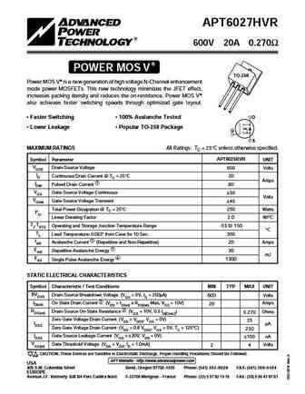
APT6027HVR 600V 20A 0.270 POWER MOS V TO-258 Power MOS V is a new generation of high voltage N-Channel enhancement mode power MOSFETs. This new technology minimizes the JFET effect, increases packing density and reduces the on-resistance. Power MOS V also achieves faster switching speeds through optimized gate layout. Faster Switching 100% Avalanche Tested D Lower
apt6025svfr.pdf

APT6025BVFR APT6025SVFR 600V 25A 0.250 POWER MOS V FREDFET D3PAK TO-247 Power MOS V is a new generation of high voltage N-Channel enhancement mode power MOSFETs. This new technology minimizes the JFET effect, increases packing density and reduces the on-resistance. Power MOS V also achieves faster switching speeds through optimized gate layout. Fast Re
apt6025bvfr.pdf
APT6025BVFR 600V 25A 0.250 POWER MOS V FREDFET Power MOS V is a new generation of high voltage N-Channel enhancement TO-247 mode power MOSFETs. This new technology minimizes the JFET effect, increases packing density and reduces the on-resistance. Power MOS V also achieves faster switching speeds through optimized gate layout. Fast Recovery Body Diode 100% Avalanche Test
apt6013jfll.pdf
APT6013JFLL 600V 39A 0.130W TM FREDFET POWER MOS 7 Power MOS 7TM is a new generation of low loss, high voltage, N-Channel enhancement mode power MOSFETS. Both conduction and switching losses are addressed with Power MOS 7TM by significantly lowering RDS(ON) and Qg. Power MOS 7TM combines lower conduction and switching losses along with exceptionally fast switching speeds inherent with
apt6010b2ll.pdf

APT6010B2LL APT6010LLL 600V 54A 0.100W B2LL TM POWER MOS 7 Power MOS 7TM is a new generation of low loss, high voltage, N-Channel T-MAX TO-264 enhancement mode power MOSFETS. Both conduction and switching losses are addressed with Power MOS 7TM by significantly lowering RDS(ON) and Qg. Power MOS 7TM combines lower conduction and switching losses along with exceptionally fast swi
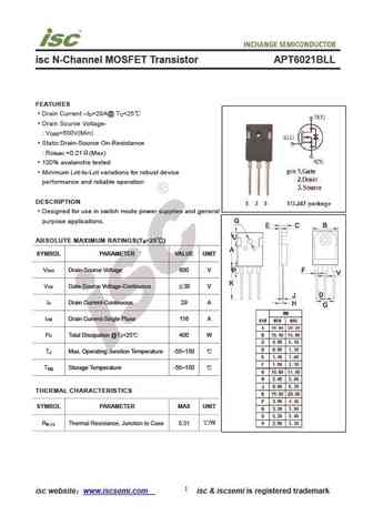
apt6021bllg.pdf
APT6021BLL APT6021SLL 600V 29A 0.210 R BLL POWER MOS 7 MOSFET D3PAK Power MOS 7 is a new generation of low loss, high voltage, N-Channel TO-247 enhancement mode power MOSFETS. Both conduction and switching losses are addressed with Power MOS 7 by significantly lowering RDS(ON) and Qg. Power MOS 7 combines lower conduction and switching losses SLL along
apt6045cvr.pdf
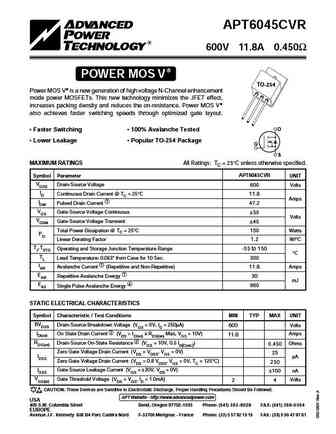
APT6045CVR 600V 11.8A 0.450 POWER MOS V TO-254 TO-254 Power MOS V is a new generation of high voltage N-Channel enhancement mode power MOSFETs. This new technology minimizes the JFET effect, increases packing density and reduces the on-resistance. Power MOS V also achieves faster switching speeds through optimized gate layout. D Faster Switching 100% Avalanche Tested
apt6011b2vfr.pdf
APT6011B2VFR 600V 49A 0.110W POWER MOS V FREDFET T-MAX Power MOS V is a new generation of high voltage N-Channel enhancement mode power MOSFETs. This new technology minimizes the JFET effect, increases packing density and reduces the on-resistance. Power MOS V also achieves faster switching speeds through optimized gate layout. Fast Recovery Body Diode 100% Avalanche Te
apt6018jn.pdf
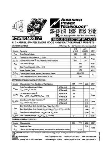
D G APT6015JN 600V 38.0A 0.15 S APT6018JN 600V 35.0A 0.18 ISOTOP "UL Recognized" File No. E145592 (S) POWER MOS IV SINGLE DIE ISOTOP PACKAGE N- CHANNEL ENHANCEMENT MODE HIGH VOLTAGE POWER MOSFETS MAXIMUM RATINGS All Ratings TC = 25 C unless otherwise specified. APT APT Symbol Parameter 6015JN 6018JN UNIT VDSS Drain-Source Voltage 600 600 Volts ID Continuous Drain Cu
apt6013jll.pdf

APT6013JLL 600V 39A 0.130W TM POWER MOS 7 Power MOS 7TM is a new generation of low loss, high voltage, N-Channel enhancement mode power MOSFETS. Both conduction and switching losses are addressed with Power MOS 7TM by significantly lowering RDS(ON) and Qg. Power MOS 7TM combines lower conduction and switching losses along with exceptionally fast switching speeds inherent with APT's "U
apt60m75jfll.pdf

APT60M75JFLL 600V 58A 0.075W TM FREDFET POWER MOS 7 Power MOS 7TM is a new generation of low loss, high voltage, N-Channel enhancement mode power MOSFETS. Both conduction and switching losses are addressed with Power MOS 7TM by significantly lowering RDS(ON) and Qg. Power MOS 7TM combines lower conduction and switching losses along with exceptionally fast switching speeds inherent wit
apt6035bvfrg apt6035svfrg.pdf
APT6035BVFR APT6035SVFR 600V 18A 0.350 BVFR POWER MOS V FREDFET D3PAK Power MOS V is a new generation of high voltage N-Channel enhancement TO-247 mode power MOSFETs. This new technology minimizes the JFET effect, increases packing density and reduces the on-resistance. Power MOS V also achieves faster switching speeds through optimized gate layout. SVFR
apt6017b2llg apt6017lllg.pdf
APT6017B2LL APT6017LLL 600V 35A 0.170 R B2LL POWER MOS 7 MOSFET T-MAX Power MOS 7 is a new generation of low loss, high voltage, N-Channel TO-264 enhancement mode power MOSFETS. Both conduction and switching losses are addressed with Power MOS 7 by significantly lowering RDS(ON) and Qg. Power MOS 7 combines lower conduction and switching losses along
apt6040bvr.pdf
APT6040BVR APT6040SVR 600V 16A 0.400 BVR POWER MOS V D3PAK TO-247 Power MOS V is a new generation of high voltage N-Channel enhancement mode power MOSFETs. This new technology minimizes the JFET effect, increases packing density and reduces the on-resistance. Power MOS V SVR also achieves faster switching speeds through optimized gate layout. D Fast
apt6038bll.pdf

APT6038BLL APT6038SLL 600V 17A 0.380W TM BLL POWER MOS 7 Power MOS 7TM is a new generation of low loss, high voltage, N-Channel D3PAK TO-247 enhancement mode power MOSFETS. Both conduction and switching losses are addressed with Power MOS 7TM by significantly lowering RDS(ON) and Qg. Power MOS 7TM combines lower conduction and switching losses along with exceptionally fast switching
apt6029bfll.pdf

APT6029BFLL APT6029SFLL 600V 21A 0.290W TM BFLL FREDFET POWER MOS 7 Power MOS 7TM is a new generation of low loss, high voltage, N-Channel D3PAK TO-247 enhancement mode power MOSFETS. Both conduction and switching losses are addressed with Power MOS 7TM by significantly lowering RDS(ON) and Qg. Power MOS 7TM combines lower conduction and switching losses along with exceptionally fas
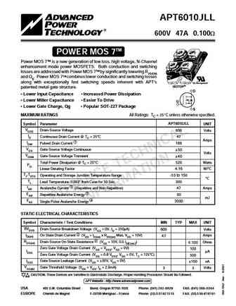
apt6010jfll.pdf
APT6010JFLL 600V 47A 0.100W TM FREDFET POWER MOS 7 Power MOS 7TM is a new generation of low loss, high voltage, N-Channel enhancement mode power MOSFETS. Both conduction and switching losses are addressed with Power MOS 7TM by significantly lowering RDS(ON) and Qg. Power MOS 7TM combines lower conduction and switching losses along with exceptionally fast switching speeds inherent with
apt60gt60jrd.pdf
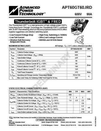
APT60GT60JRD 600V 90A Thunderbolt IGBT & FRED The Thunderbolt IGBT is a new generation of high voltage power IGBTs. Using Non-Punch Through Technology the Thunderbolt IGBT combined with an APT free-wheeling ultraFast Recovery Epitaxial Diode (FRED) offers superior ruggedness and ultrafast switching speed. "UL Recognized" ISOTOP Low Forward Voltage Drop High Freq. Swi
apt6040svr.pdf

APT6040BVR APT6040SVR 600V 16A 0.400 BVR POWER MOS V D3PAK TO-247 Power MOS V is a new generation of high voltage N-Channel enhancement mode power MOSFETs. This new technology minimizes the JFET effect, increases packing density and reduces the on-resistance. Power MOS V SVR also achieves faster switching speeds through optimized gate layout. D Fast
apt60m80l2vfrg.pdf
APT60M80L2VFR 600V 65A 0.080 POWER MOS V FREDFET L2VFR TO-264 Max Power MOS V is a new generation of high voltage N-Channel enhancement mode power MOSFETs. This new technology minimizes the JFET effect, increases packing density and reduces the on-resistance. Power MOS V also achieves faster switching speeds through optimized gate layout. TO-264 MAX P
apt6015jn.pdf
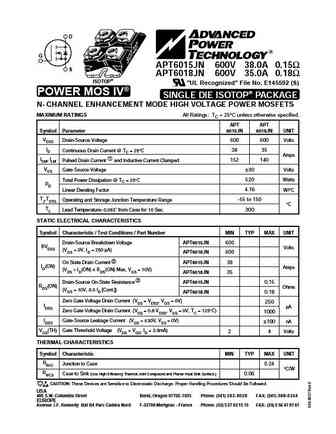
D G APT6015JN 600V 38.0A 0.15 S APT6018JN 600V 35.0A 0.18 ISOTOP "UL Recognized" File No. E145592 (S) POWER MOS IV SINGLE DIE ISOTOP PACKAGE N- CHANNEL ENHANCEMENT MODE HIGH VOLTAGE POWER MOSFETS MAXIMUM RATINGS All Ratings TC = 25 C unless otherwise specified. APT APT Symbol Parameter 6015JN 6018JN UNIT VDSS Drain-Source Voltage 600 600 Volts ID Continuous Drain Cu
apt60m90jn.pdf
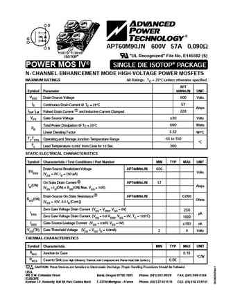
D G APT60M90JN 600V 57A 0.090 S "UL Recognized" File No. E145592 (S) ISOTOP SINGLE DIE ISOTOP PACKAGE POWER MOS IV N- CHANNEL ENHANCEMENT MODE HIGH VOLTAGE POWER MOSFETS MAXIMUM RATINGS All Ratings TC = 25 C unless otherwise specified. APT Symbol Parameter 60M90JN UNIT VDSS Drain-Source Voltage 600 Volts ID Continuous Drain Current @ TC = 25 C 57 Amps IDM, lLM Pulse
apt60gu30b.pdf
TYPICAL PERFORMANCE CURVES APT60GU30B_S APT60GU30B APT60GU30S 300V POWER MOS 7 IGBT TO-247 The POWER MOS 7 IGBT is a new generation of high voltage power IGBTs. D3PAK Using Punch Through Technology this IGBT is ideal for many high frequency, high voltage switching applications and has been optimized for high frequency C switchmode power supplies. G E G C Low Conductio
apt60m75jvr.pdf
APT60M75JVR 600V 62A 0.075 POWER MOS V Power MOS V is a new generation of high voltage N-Channel enhancement mode power MOSFETs. This new technology minimizes the JFET effect, increases packing density and reduces the on-resistance. Power MOS V also achieves faster switching speeds through optimized gate layout. "UL Recognized" ISOTOP D Faster Switching 100% Avalanc
apt6021bfllg apt6021sfllg.pdf
APT6021BFLL APT6021SFLL 600V 29A 0.210 R BFLL POWER MOS 7 FREDFET D3PAK Power MOS 7 is a new generation of low loss, high voltage, N-Channel TO-247 enhancement mode power MOSFETS. Both conduction and switching losses are addressed with Power MOS 7 by significantly lowering RDS(ON) and Qg. Power MOS 7 combines lower conduction and switching losses SFLL
apt60m75.pdf

APT60M75JVR 600V 62A 0.075 POWER MOS V Power MOS V is a new generation of high voltage N-Channel enhancement mode power MOSFETs. This new technology minimizes the JFET effect, increases packing density and reduces the on-resistance. Power MOS V also achieves faster switching speeds through optimized gate layout. "UL Recognized" ISOTOP D Faster Switching 100% Avalanc
apt6013b2fllg apt6013lfllg.pdf
APT6013B2FLL APT6013LFLL 600V 43A 0.130 B2FLL R POWER MOS 7 FREDFET T-MAX TO-264 Power MOS 7 is a new generation of low loss, high voltage, N-Channel enhancement mode power MOSFETS. Both conduction and switching losses are addressed with Power MOS 7 by significantly lowering RDS(ON) and Qg. Power MOS 7 combines lower conduction and switching losses L
apt6021bll.pdf
APT6021BLL APT6021SLL 600V 29A 0.210W TM BLL POWER MOS 7 Power MOS 7TM is a new generation of low loss, high voltage, N-Channel D3PAK TO-247 enhancement mode power MOSFETS. Both conduction and switching losses are addressed with Power MOS 7TM by significantly lowering RDS(ON) and Qg. Power MOS 7TM combines lower conduction and switching losses along with exceptionally fast switching
apt60m75jll.pdf
APT60M75JLL 600V 58A 0.075W TM POWER MOS 7 Power MOS 7TM is a new generation of low loss, high voltage, N-Channel enhancement mode power MOSFETS. Both conduction and switching losses are addressed with Power MOS 7TM by significantly lowering RDS(ON) and Qg. Power MOS 7TM combines lower conduction and switching losses along with exceptionally fast switching speeds inherent with APT's "
apt6015.pdf
APT6015B2VR 600V 38A 0.150 POWER MOS V T-MAX Power MOS V is a new generation of high voltage N-Channel enhancement mode power MOSFETs. This new technology minimizes the JFET effect, increases packing density and reduces the on-resistance. Power MOS V also achieves faster switching speeds through optimized gate layout. Faster Switching 100% Avalanche Tested D Low
apt6038bfllg apt6038sfllg.pdf

APT6038BFLL APT6038SFLL 600V 17A 0.380 R BFLL POWER MOS 7 FREDFET D3PAK Power MOS 7 is a new generation of low loss, high voltage, N-Channel TO-247 enhancement mode power MOSFETS. Both conduction and switching losses are addressed with Power MOS 7 by significantly lowering RDS(ON) and Qg. Power MOS 7 combines lower conduction and switching losses SFLL a
apt60m75pvr.pdf
APT60M75PVR 600V 60.5A 0.075 POWER MOS V P-Pack Power MOS V is a new generation of high voltage N-Channel enhancement mode power MOSFETs. This new technology minimizes the JFET effect, increases packing density and reduces the on-resistance. Power MOS V also achieves faster switching speeds through optimized gate layout. Faster Switching 100% Avalanche Tested D Low
apt6011lvfr.pdf
APT6011LVFR 600V 49A 0.110W POWER MOS V FREDFET Power MOS V is a new generation of high voltage N-Channel enhancement TO-264 mode power MOSFETs. This new technology minimizes the JFET effect, increases packing density and reduces the on-resistance. Power MOS V also achieves faster switching speeds through optimized gate layout. Fast Recovery Body Diode 100% Avalanche Teste
apt6029sll apt6029sllg.pdf

APT6029BLL APT6029SLL 600V 21A 0.290 R BLL POWER MOS 7 MOSFET D3PAK Power MOS 7 is a new generation of low loss, high voltage, N-Channel TO-247 enhancement mode power MOSFETS. Both conduction and switching losses are addressed with Power MOS 7 by significantly lowering RDS(ON) and Qg. Power MOS 7 combines lower conduction and switching losses SLL along
apt6025bvr.pdf
APT6025BVR 600V 25A 0.250 POWER MOS V Power MOS V is a new generation of high voltage N-Channel enhancement TO-247 mode power MOSFETs. This new technology minimizes the JFET effect, increases packing density and reduces the on-resistance. Power MOS V also achieves faster switching speeds through optimized gate layout. Faster Switching 100% Avalanche Tested D Lower L
apt6029bll.pdf

APT6029BLL APT6029SLL 600V 21A 0.290W TM BLL POWER MOS 7 Power MOS 7TM is a new generation of low loss, high voltage, N-Channel D3PAK TO-247 enhancement mode power MOSFETS. Both conduction and switching losses are addressed with Power MOS 7TM by significantly lowering RDS(ON) and Qg. Power MOS 7TM combines lower conduction and switching losses along with exceptionally fast switching
apt6040.pdf

D TO-247 G APT6040BN 600V 18.0A 0.40 S APT6045BN 600V 17.0A 0.45 POWER MOS IV N- CHANNEL ENHANCEMENT MODE HIGH VOLTAGE POWER MOSFETS MAXIMUM RATINGS All Ratings TC = 25 C unless otherwise specified. APT APT Symbol Parameter 6040BN 6045BN UNIT VDSS Drain-Source Voltage 600 600 Volts ID Continuous Drain Current @ TC = 25 C 18 17 Amps IDM Pulsed Drain Current 1 72 68 V
apt6045svr.pdf
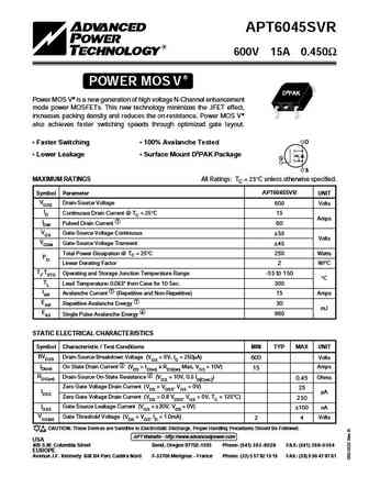
APT6045SVR 600V 15A 0.450 POWER MOS V D3PAK Power MOS V is a new generation of high voltage N-Channel enhancement mode power MOSFETs. This new technology minimizes the JFET effect, increases packing density and reduces the on-resistance. Power MOS V also achieves faster switching speeds through optimized gate layout. D Faster Switching 100% Avalanche Tested Lower
apt6038bllg apt6038sllg.pdf

APT6038BLL APT6038SLL 600V 17A 0.380 R BLL POWER MOS 7 MOSFET D3PAK TO-247 Power MOS 7 is a new generation of low loss, high voltage, N-Channel enhancement mode power MOSFETS. Both conduction and switching losses are addressed with Power MOS 7 by significantly lowering RDS(ON) and Qg. Power MOS 7 combines lower conduction and switching losses SLL along
apt6010jll.pdf
APT6010JLL 600V 47A 0.100W TM POWER MOS 7 Power MOS 7TM is a new generation of low loss, high voltage, N-Channel enhancement mode power MOSFETS. Both conduction and switching losses are addressed with Power MOS 7TM by significantly lowering RDS(ON) and Qg. Power MOS 7TM combines lower conduction and switching losses along with exceptionally fast switching speeds inherent with APT's "U
apt6021bfll.pdf

APT6021BFLL APT6021SFLL 600V 29A 0.210W TM BFLL FREDFET POWER MOS 7 Power MOS 7TM is a new generation of low loss, high voltage, N-Channel D3PAK TO-247 enhancement mode power MOSFETS. Both conduction and switching losses are addressed with Power MOS 7TM by significantly lowering RDS(ON) and Qg. Power MOS 7TM combines lower conduction and switching losses along with exceptionally fas
apt6015b2vfrg apt6015lvfrg.pdf
APT6015B2VFR APT6015LVFR 600V 38A 0.150 B2VFR POWER MOS V FREDFET T-MAX TO-264 Power MOS V is a new generation of high voltage N-Channel enhancement mode power MOSFETs. This new technology minimizes the JFET effect, increases packing density and reduces the on-resistance. Power MOS V also achieves faster switching speeds through optimized gate layout.
apt6035bvfr.pdf

APT6035BVFR APT6035SVFR 600V 18A 0.350 BVFR POWER MOS V FREDFET D3PAK Power MOS V is a new generation of high voltage N-Channel enhancement TO-247 mode power MOSFETs. This new technology minimizes the JFET effect, increases packing density and reduces the on-resistance. Power MOS V also achieves faster switching speeds through optimized gate layout. SVFR
apt6017jfll.pdf

APT6017JFLL 600V 31A 0.170W TM FREDFET POWER MOS 7 Power MOS 7TM is a new generation of low loss, high voltage, N-Channel enhancement mode power MOSFETS. Both conduction and switching losses are addressed with Power MOS 7TM by significantly lowering RDS(ON) and Qg. Power MOS 7TM combines lower conduction and switching losses along with exceptionally fast switching speeds inherent with
apt6035svr.pdf

APT6035SVR 600V 18A 0.350 POWER MOS V D3PAK Power MOS V is a new generation of high voltage N-Channel enhancement mode power MOSFETs. This new technology minimizes the JFET effect, increases packing density and reduces the on-resistance. Power MOS V also achieves faster switching speeds through optimized gate layout. D Faster Switching 100% Avalanche Tested Lower
apt6030bn.pdf
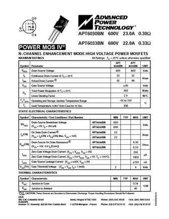
D TO-247 G APT6030BN 600V 23.0A 0.30 S APT6033BN 600V 22.0A 0.33 POWER MOS IV N- CHANNEL ENHANCEMENT MODE HIGH VOLTAGE POWER MOSFETS MAXIMUM RATINGS All Ratings TC = 25 C unless otherwise specified. APT APT Symbol Parameter 6030BN 6033BN UNIT VDSS Drain-Source Voltage 600 600 Volts ID Continuous Drain Current @ TC = 25 C 23 22 Amps IDM Pulsed Drain Current 1 92 88 V
apt6017b2fll.pdf
APT6017B2FLL APT6017LFLL 600V 35A 0.017W TM FREDFET POWER MOS 7 B2FLL Power MOS 7TM is a new generation of low loss, high voltage, N-Channel enhancement mode power MOSFETS. Both conduction and switching T-MAX TO-264 losses are addressed with Power MOS 7TM by significantly lowering RDS(ON) and Qg. Power MOS 7TM combines lower conduction and switching losses along with exceptiona
apt6025bfll.pdf
APT6025BFLL APT6025SFLL 600V 24A 0.250W TM BFLL FREDFET POWER MOS 7 Power MOS 7TM is a new generation of low loss, high voltage, N-Channel D3PAK TO-247 enhancement mode power MOSFETS. Both conduction and switching losses are addressed with Power MOS 7TM by significantly lowering RDS(ON) and Qg. Power MOS 7TM combines lower conduction and switching losses along with exceptionally fas
apt6017jll.pdf

APT6017JLL 600V 31A 0.170W TM POWER MOS 7 Power MOS 7TM is a new generation of low loss, high voltage, N-Channel enhancement mode power MOSFETS. Both conduction and switching losses are addressed with Power MOS 7TM by significantly lowering RDS(ON) and Qg. Power MOS 7TM combines lower conduction and switching losses along with exceptionally fast switching speeds inherent with APT's "U
apt60m75l2fll.pdf
APT60M75L2FLL 600V 73A 0.075W TM FREDFET POWER MOS 7 Power MOS 7TM is a new generation of low loss, high voltage, N-Channel TO-264 Max enhancement mode power MOSFETS. Both conduction and switching losses are addressed with Power MOS 7TM by significantly lowering RDS(ON) and Qg. Power MOS 7TM combines lower conduction and switching losses along with exceptionally fast switching speeds
apt6030.pdf

APT6030BVFR 600V 21A 0.300W POWER MOS V FREDFET Power MOS V is a new generation of high voltage N-Channel enhancement TO-247 mode power MOSFETs. This new technology minimizes the JFET effect, increases packing density and reduces the on-resistance. Power MOS V also achieves faster switching speeds through optimized gate layout. Fast Recovery Body Diode 100% Avalanche Tested
apt6040svfr.pdf
600V 16A 0.40 APT6040BVFR APT6040SVFR APT6040BVFRG*APT6040SVFRG* *G Denotes RoHS Compliant, Pb Free Terminal Finish. BVFR POWER MOS V FREDFET D3PAK Power MOS V is a new generation of high voltage N-Channel enhancement TO-247 mode power MOSFETs. This new technology minimizes the JFET effect, increases packing density and reduces the on-resistance. Power MOS
apt60m60jll.pdf
APT60M60JLL 600V 70A 0.060W TM POWER MOS 7 Power MOS 7TM is a new generation of low loss, high voltage, N-Channel enhancement mode power MOSFETS. Both conduction and switching losses are addressed with Power MOS 7TM by significantly lowering RDS(ON) and Qg. Power MOS 7TM combines lower conduction and switching losses along with exceptionally fast switching speeds inherent with APT's "
apt6020lvr.pdf
APT6020LVR 600V 30A 0.200 POWER MOS V Power MOS V is a new generation of high voltage N-Channel enhancement TO-264 mode power MOSFETs. This new technology minimizes the JFET effect, increases packing density and reduces the on-resistance. Power MOS V also achieves faster switching speeds through optimized gate layout.. Faster Switching 100% Avalanche Tested D Lower
apt6035avr.pdf
APT6035AVR 600V 16A 0.350 POWER MOS V TO-3 Power MOS V is a new generation of high voltage N-Channel enhancement mode power MOSFETs. This new technology minimizes the JFET effect, increases packing density and reduces the on-resistance. Power MOS V also achieves faster switching speeds through optimized gate layout. D Faster Switching 100% Avalanche Tested Lower L
apt6025svr.pdf
APT6025SVR 600V 25A 0.250W POWER MOS V D3PAK Power MOS V is a new generation of high voltage N-Channel enhancement mode power MOSFETs. This new technology minimizes the JFET effect, increases packing density and reduces the on-resistance. Power MOS V also achieves faster switching speeds through optimized gate layout. D Faster Switching 100% Avalanche Tested Lower Le
apt6015jvfr.pdf
APT6015JVFR 600V 35A 0.150W FREDFET POWER MOS V Power MOS V is a new generation of high voltage N-Channel enhance- ment mode power MOSFETs. This new technology minimizes the JFET ef- fect, increases packing density and reduces the on-resistance. Power MOS V also achieves faster switching speeds through optimized gate layout. "UL Recognized" ISOTOP file # E145592 Faster S
apt6010b2fllg apt6010lfllg.pdf
600V 54A 0.100 APT6010B2FLL APT6010LFLL APT6010B2FLL* APT6010LFLLG* *G Denotes RoHS Compliant, Pb Free Terminal Finish. R B2FLL POWER MOS 7 FREDFET T-MAX TO-264 Power MOS 7 is a new generation of low loss, high voltage, N-Channel enhancement mode power MOSFETS. Both conduction and switching losses are addressed with Power MOS 7 by significantly lowering
apt60ga60jd60.pdf
APT60GA60JD60 600V High Speed PT IGBT POWER MOS 8 is a high speed Punch-Through switch-mode IGBT. Low Eoff is achieved through leading technology silicon design and lifetime control processes. A reduced Eoff - VCE(ON) tradeoff results in superior efficiency compared to other IGBT technologies. Low gate charge and a greatly reduced ratio of Cres/Cies provide excellent noise immunity
apt6045bvfrg apt6045svfrg.pdf
APT6045BVFR APT6045SVFR APT6045BVFRG APT6045SVFRG 600V 15A 0.45 *G Denotes RoHS Compliant, Pb Free Terminal Finish. BVFR POWER MOS V FREDFET Power MOS V is a new generation of high voltage N-Channel enhance- D3PAK ment mode power MOSFETs. This new technology minimizes the JFET ef- fect, increases packing density and reduces the on-resistance. Power MOS V also achieves
apt60n90jc3.pdf
900V 60A APT60N90JC3 COOLMOS Power Semiconductors Super Junction MOSFET Ultra Low RDS(ON) Low Miller Capacitance Ultra Low Gate Charge, Qg "UL Recognized" ISOTOP file # E145592 Avalanche Energy Rated D Extreme dv/dt Rated Dual die (parallel) G Popular T-MAX Package S Unless stated otherwise, Microsemi discrete MOSFETs contain a single MOSFET
apt60n60bcsg.pdf
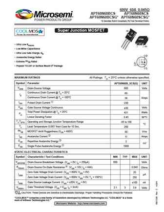
600V 60A 0.045 APT60N60BCS APT60N60SCS APT60N60BCSG* APT60N60SCSG* *G Denotes RoHS Compliant, Pb Free Terminal Finish. Super Junction MOSFET (B) COOLMOS Po we r Se miconduc tors D3PAK Ultra Low RDS(ON) (S) Low Miller Capacitance Ultra Low Gate Charge, Qg D Avalanche Energy Rated Extreme dv/dt Rated G Popular TO-247 or Surface Mount D3 Package
apt60gt60brg apt60gt60srg.pdf
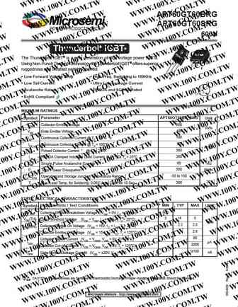
APT60GT60BRG APT60GT60SRG 600V (B) Thunderbolt IGBT D3PAK The Thunderbolt IGBT is a new generation of high voltage power IGBTs. (S) Using Non-Punch Through Technology the Thunderbolt IGBT offers superior C G E ruggedness and ultrafast switching speed. G C Low Forward Voltage Drop High Freq. Switching to 150KHz E Low Tail Current Ultra Low Leakage Curre
apt6010b2llg apt6010lllg.pdf
600V 54A 0.100 APT6010B2LL APT6010LLL APT6010B2LL* APT6010LLLG* *G Denotes RoHS Compliant, Pb Free Terminal Finish. R B2LL POWER MOS 7 MOSFET T-MAX Power MOS 7 is a new generation of low loss, high voltage, N-Channel TO-264 enhancement mode power MOSFETS. Both conduction and switching losses are addressed with Power MOS 7 by significantly lowering RDS(O
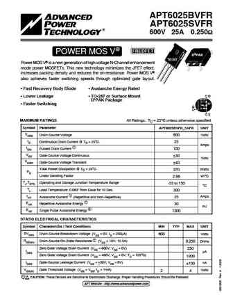
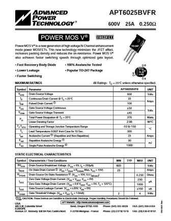
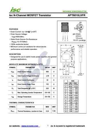
apt6045bvr.pdf

isc N-Channel MOSFET Transistor APT6045BVR FEATURES Drain Current I =15A@ T =25 D C Drain Source Voltage- V =600V(Min) DSS Static Drain-Source On-Resistance R =0.45 (Max) DS(on) 100% avalanche tested Minimum Lot-to-Lot variations for robust device performance and reliable operation DESCRIPTION Designed for use in switch mode power supplies and general purpo
apt6030bvr.pdf

isc N-Channel MOSFET Transistor APT6030BVR FEATURES Drain Current I =21A@ T =25 D C Drain Source Voltage- V =600V(Min) DSS Static Drain-Source On-Resistance R =0.3 (Max) DS(on) 100% avalanche tested Minimum Lot-to-Lot variations for robust device performance and reliable operation DESCRIPTION Designed for use in switch mode power supplies and general purpos
apt6013b2fll.pdf

isc N-Channel MOSFET Transistor APT6013B2FLL FEATURES Drain Current I = 43A@ T =25 D C Drain Source Voltage- V =600V(Min) DSS Static Drain-Source On-Resistance R =0.13 (Max) DS(on) 100% avalanche tested Minimum Lot-to-Lot variations for robust device performance and reliable operation DESCRIPTION Designed for use in switch mode power supplies and general pu
apt6015lvfr.pdf
isc N-Channel MOSFET Transistor APT6015LVFR FEATURES Drain Current I = 38A@ T =25 D C Drain Source Voltage- V =600V(Min) DSS Static Drain-Source On-Resistance R =0.15 (Max) DS(on) 100% avalanche tested Minimum Lot-to-Lot variations for robust device performance and reliable operation DESCRIPTION Designed for use in switch mode power supplies and general pur
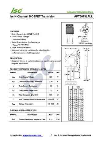
apt6017lfll.pdf
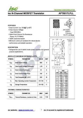
isc N-Channel MOSFET Transistor APT6017LFLL FEATURES Drain Current I = 35A@ T =25 D C Drain Source Voltage- V =600V(Min) DSS Static Drain-Source On-Resistance R =0.17 (Max) DS(on) 100% avalanche tested Minimum Lot-to-Lot variations for robust device performance and reliable operation DESCRIPTION Designed for use in switch mode power supplies and general pur
apt6025bll.pdf

isc N-Channel MOSFET Transistor APT6025BLL FEATURES Drain Current I =24A@ T =25 D C Drain Source Voltage- V =600V(Min) DSS Static Drain-Source On-Resistance R =0.25 (Max) DS(on) 100% avalanche tested Minimum Lot-to-Lot variations for robust device performance and reliable operation DESCRIPTION Designed for use in switch mode power supplies and general purpo
apt6035bvr.pdf

isc N-Channel MOSFET Transistor APT6035BVR FEATURES Drain Current I =18A@ T =25 D C Drain Source Voltage- V =600V(Min) DSS Static Drain-Source On-Resistance R =0.35 (Max) DS(on) 100% avalanche tested Minimum Lot-to-Lot variations for robust device performance and reliable operation DESCRIPTION Designed for use in switch mode power supplies and general purpo
apt6010b2fll.pdf

isc N-Channel MOSFET Transistor APT6010B2FLL FEATURES Drain Current I = 54A@ T =25 D C Drain Source Voltage- V =600V(Min) DSS Static Drain-Source On-Resistance R =0.1 (Max) DS(on) 100% avalanche tested Minimum Lot-to-Lot variations for robust device performance and reliable operation DESCRIPTION Designed for use in switch mode power supplies and general pur
apt6010lfll.pdf

isc N-Channel MOSFET Transistor APT6010LFLL FEATURES Drain Current I = 54A@ T =25 D C Drain Source Voltage- V =600V(Min) DSS Static Drain-Source On-Resistance R =0.1 (Max) DS(on) 100% avalanche tested Minimum Lot-to-Lot variations for robust device performance and reliable operation DESCRIPTION Designed for use in switch mode power supplies and general purp
apt6013b2ll.pdf

isc N-Channel MOSFET Transistor APT6013B2LL FEATURES Drain Current I = 43A@ T =25 D C Drain Source Voltage- V =600V(Min) DSS Static Drain-Source On-Resistance R =0.13 (Max) DS(on) 100% avalanche tested Minimum Lot-to-Lot variations for robust device performance and reliable operation DESCRIPTION Designed for use in switch mode power supplies and general pur
apt60n60bcs.pdf

isc N-Channel MOSFET Transistor APT60N60BCS FEATURES Drain Current I =60A@ T =25 D C Drain Source Voltage- V =600V(Min) DSS Static Drain-Source On-Resistance R =0.045 (Max) DS(on) 100% avalanche tested Minimum Lot-to-Lot variations for robust device performance and reliable operation DESCRIPTION Designed for use in switch mode power supplies and general pur
apt6015b2vfr.pdf

isc N-Channel MOSFET Transistor APT6015B2VFR FEATURES Drain Current I = 38A@ T =25 D C Drain Source Voltage- V =600V(Min) DSS Static Drain-Source On-Resistance R =0.15 (Max) DS(on) 100% avalanche tested Minimum Lot-to-Lot variations for robust device performance and reliable operation DESCRIPTION Designed for use in switch mode power supplies and general pu
apt6030bvfr.pdf

isc N-Channel MOSFET Transistor APT6030BVFR FEATURES Drain Current I =21A@ T =25 D C Drain Source Voltage- V =600V(Min) DSS Static Drain-Source On-Resistance R =0.3 (Max) DS(on) 100% avalanche tested Minimum Lot-to-Lot variations for robust device performance and reliable operation DESCRIPTION Designed for use in switch mode power supplies and general purpo
apt6038bfll.pdf

isc N-Channel MOSFET Transistor APT6038BFLL FEATURES Drain Current I =17A@ T =25 D C Drain Source Voltage- V =600V(Min) DSS Static Drain-Source On-Resistance R =0.38 (Max) DS(on) 100% avalanche tested Minimum Lot-to-Lot variations for robust device performance and reliable operation DESCRIPTION Designed for use in switch mode power supplies and general purp
apt6025bvfr.pdf

isc N-Channel MOSFET Transistor APT6025BVFR FEATURES Drain Current I =25A@ T =25 D C Drain Source Voltage- V =600V(Min) DSS Static Drain-Source On-Resistance R =0.25 (Max) DS(on) 100% avalanche tested Minimum Lot-to-Lot variations for robust device performance and reliable operation DESCRIPTION Designed for use in switch mode power supplies and general purp
apt6010b2ll.pdf

isc N-Channel MOSFET Transistor APT6010B2LL FEATURES Drain Current I = 54A@ T =25 D C Drain Source Voltage- V =600V(Min) DSS Static Drain-Source On-Resistance R =0.1 (Max) DS(on) 100% avalanche tested Minimum Lot-to-Lot variations for robust device performance and reliable operation DESCRIPTION Designed for use in switch mode power supplies and general purp
apt6038bll.pdf

isc N-Channel MOSFET Transistor APT6038BLL FEATURES Drain Current I =17A@ T =25 D C Drain Source Voltage- V =600V(Min) DSS Static Drain-Source On-Resistance R =0.38 (Max) DS(on) 100% avalanche tested Minimum Lot-to-Lot variations for robust device performance and reliable operation DESCRIPTION Designed for use in switch mode power supplies and general purpo
apt6029bfll.pdf

isc N-Channel MOSFET Transistor APT6029BFLL FEATURES Drain Current I =21A@ T =25 D C Drain Source Voltage- V =600V(Min) DSS Static Drain-Source On-Resistance R =0.29 (Max) DS(on) 100% avalanche tested Minimum Lot-to-Lot variations for robust device performance and reliable operation DESCRIPTION Designed for use in switch mode power supplies and general purp
apt6021bll.pdf
isc N-Channel MOSFET Transistor APT6021BLL FEATURES Drain Current I =29A@ T =25 D C Drain Source Voltage- V =600V(Min) DSS Static Drain-Source On-Resistance R =0.21 (Max) DS(on) 100% avalanche tested Minimum Lot-to-Lot variations for robust device performance and reliable operation DESCRIPTION Designed for use in switch mode power supplies and general purpo
apt6025bvr.pdf

isc N-Channel MOSFET Transistor APT6025BVR FEATURES Drain Current I =25A@ T =25 D C Drain Source Voltage- V =600V(Min) DSS Static Drain-Source On-Resistance R =0.25 (Max) DS(on) 100% avalanche tested Minimum Lot-to-Lot variations for robust device performance and reliable operation DESCRIPTION Designed for use in switch mode power supplies and general purpo
apt6029bll.pdf

isc N-Channel MOSFET Transistor APT6029BLL FEATURES Drain Current I =21A@ T =25 D C Drain Source Voltage- V =600V(Min) DSS Static Drain-Source On-Resistance R =0.29 (Max) DS(on) 100% avalanche tested Minimum Lot-to-Lot variations for robust device performance and reliable operation DESCRIPTION Designed for use in switch mode power supplies and general purpo
apt6013lfll.pdf
isc N-Channel MOSFET Transistor APT6013LFLL FEATURES Drain Current I = 43A@ T =25 D C Drain Source Voltage- V =600V(Min) DSS Static Drain-Source On-Resistance R =0.13 (Max) DS(on) 100% avalanche tested Minimum Lot-to-Lot variations for robust device performance and reliable operation DESCRIPTION Designed for use in switch mode power supplies and general pur
apt6021bfll.pdf

isc N-Channel MOSFET Transistor APT6021BFLL FEATURES Drain Current I =29A@ T =25 D C Drain Source Voltage- V =600V(Min) DSS Static Drain-Source On-Resistance R =0.21 (Max) DS(on) 100% avalanche tested Minimum Lot-to-Lot variations for robust device performance and reliable operation DESCRIPTION Designed for use in switch mode power supplies and general purp
apt6017b2fll.pdf
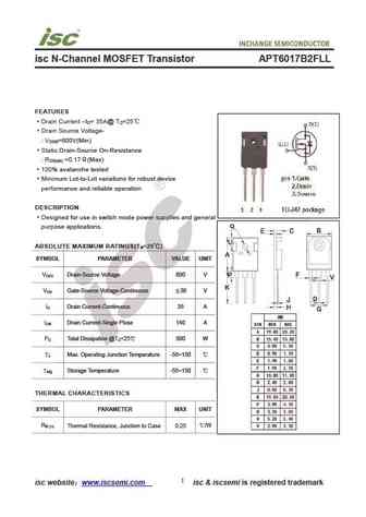
isc N-Channel MOSFET Transistor APT6017B2FLL FEATURES Drain Current I = 35A@ T =25 D C Drain Source Voltage- V =600V(Min) DSS Static Drain-Source On-Resistance R =0.17 (Max) DS(on) 100% avalanche tested Minimum Lot-to-Lot variations for robust device performance and reliable operation DESCRIPTION Designed for use in switch mode power supplies and general pu
apt6025bfll.pdf

isc N-Channel MOSFET Transistor APT6025BFLL FEATURES Drain Current I =24A@ T =25 D C Drain Source Voltage- V =600V(Min) DSS Static Drain-Source On-Resistance R =0.25 (Max) DS(on) 100% avalanche tested Minimum Lot-to-Lot variations for robust device performance and reliable operation DESCRIPTION Designed for use in switch mode power supplies and general purp
apt60m75l2fll.pdf
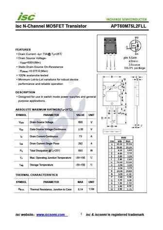
isc N-Channel MOSFET Transistor APT60M75L2FLL FEATURES Drain Current I = 73A@ T =25 D C Drain Source Voltage- V =600V(Min) DSS Static Drain-Source On-Resistance R =0.075 (Max) DS(on) 100% avalanche tested Minimum Lot-to-Lot variations for robust device performance and reliable operation DESCRIPTION Designed for use in switch mode power supplies and general
Другие IGBT... APT6038SFLLG, APT6038SLLG, APT6040SVFR, APT6040SVR, APT6045BN, APT6045BVFRG, APT6045SVFRG, APT6060AN, 7N60, APT60M75JVFR, APT60M75L2FLLG, APT60M75L2LLG, APT60M80L2VFRG, APT60M80L2VRG, APT60N60BCSG, APT60N90JC3, APT66F60B2
Параметры MOSFET. Взаимосвязь и компромиссы
History: HTD760P10T | IXFK64N60P | FDS4935BZ | HM70N90D | DHS015N06E | HM6409 | HM8205Q
🌐 : EN ES РУ

Список транзисторов
Обновления
MOSFET: CS95118 | CS85105A | CS75N45 | CS72N12 | CS55N50 | CS48N75A | CS40N27 | MSQ60P04D | MSQ40P07D | MSQ30P40D | MSQ30P15 | MSQ30P07D | MSQ100N03D | MSHM60P14 | MSHM40N085 | MSHM30N46
Popular searches
2sb649 | 2sb324 transistor | b754 transistor | 2sc828 equivalent | 4843ns | 2sc1318 datasheet | 2sc3281 datasheet | 2sa1106