APT7590AN datasheet, аналоги, основные параметры
Наименование производителя: APT7590AN 📄📄
Тип транзистора: MOFETS
Полярность: N
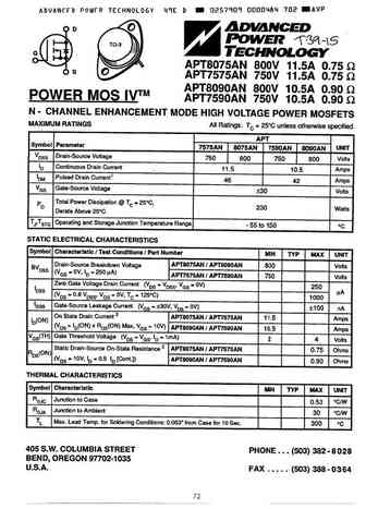
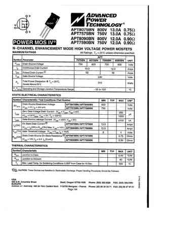
Предельные значения
Pd ⓘ - Максимальная рассеиваемая мощность: 230 W
|Vds|ⓘ - Максимально допустимое напряжение сток-исток: 750 V
|Vgs|ⓘ - Максимально допустимое напряжение затвор-исток: 30 V
|Id| ⓘ - Максимально допустимый постоянный ток стока: 10.5 A
Tj ⓘ - Максимальная температура канала: 150 °C
Электрические характеристики
tr ⓘ - Время нарастания: 18 ns
Cossⓘ - Выходная емкость: 370 pf
RDSonⓘ - Сопротивление сток-исток открытого транзистора: 0.9 Ohm
Тип корпуса: TO-3
📄📄 Копировать
Аналог (замена) для APT7590AN
- подборⓘ MOSFET транзистора по параметрам
APT7590AN даташит
9.1. Size:82K apt
apt75gn120b2g.pdf 
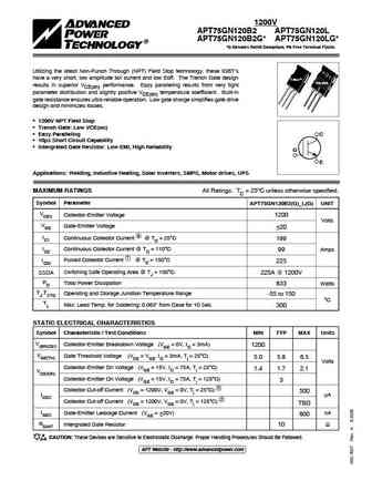
TYPICAL PERFORMANCE CURVES APT75GN120B2(G)_L(G) 1200V APT75GN120B2 APT75GN120L APT75GN120B2G* APT75GN120LG* *G Denotes RoHS Compliant, Pb Free Terminal Finish. Utilizing the latest Non-Punch Through (NPT) Field Stop technology, these IGBT s have a very short, low amplitude tail current and low Eoff. The Trench Gate design T-Max TO-264 results in superior VCE(on) perform
9.2. Size:453K apt
apt75gp120jdq3.pdf 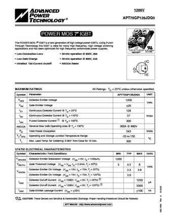
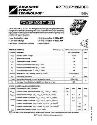
TYPICAL PERFORMANCE CURVES APT75GP120JDQ3 1200V APT75GP120JDQ3 POWER MOS 7 IGBT The POWER MOS 7 IGBT is a new generation of high voltage power IGBTs. Using Punch Through Technology this IGBT is ideal for many high frequency, high voltage switching applications and has been optimized for high frequency switchmode power supplies. "UL Recognized" ISOTOP file # E145592
9.3. Size:436K apt
apt75gn60ldq3g.pdf 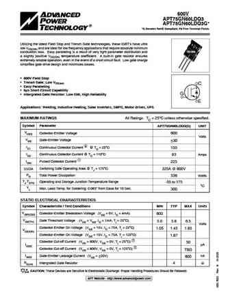
TYPICAL PERFORMANCE CURVES APT75GN60LDQ3(G) 600V APT75GN60LDQ3 APT75GN60LDQ3G* *G Denotes RoHS Compliant, Pb Free Terminal Finish. Utilizing the latest Field Stop and Trench Gate technologies, these IGBT's have ultra low VCE(ON) and are ideal for low frequency applications that require absolute minimum TO-264 conduction loss. Easy paralleling is a result of very tight parameter
9.4. Size:399K apt
apt75gn60bg.pdf 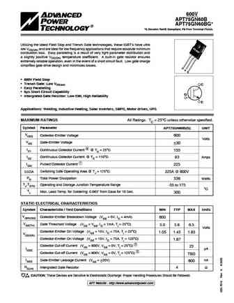
TYPICAL PERFORMANCE CURVES APT75GN60B(G) 600V APT75GN60B APT75GN60BG* *G Denotes RoHS Compliant, Pb Free Terminal Finish. Utilizing the latest Field Stop and Trench Gate technologies, these IGBT's have ultra low VCE(ON) and are ideal for low frequency applications that require absolute minimum conduction loss. Easy paralleling is a result of very tight parameter distribution and
9.5. Size:33K apt
apt75gp120j.pdf 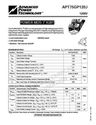
APT75GP120J 1200V POWER MOS 7 IGBT The POWER MOS 7 IGBT is a new generation of high voltage power IGBTs. Using Punch Through Technology this IGBT is ideal for many high frequency, "UL Recognized" high voltage switching applications and has been optimized for high frequency ISOTOP switchmode power supplies. C Low Conduction Loss RBSOA rated Low Gate Charge G
9.6. Size:94K apt
apt75gp120b2.pdf 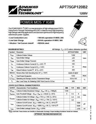
APT75GP120B2 1200V POWER MOS 7 IGBT T-MaxTM The POWER MOS 7 IGBT is a new generation of high voltage power IGBTs. Using Punch Through Technology this IGBT is ideal for many high frequency, high voltage switching applications and has been optimized for high frequency switchmode power supplies. G C E C Low Conduction Loss 100 kHz operation @ 800V, 20A Low Gate Char
9.7. Size:82K apt
apt75gn120lg.pdf 
TYPICAL PERFORMANCE CURVES APT75GN120B2(G)_L(G) 1200V APT75GN120B2 APT75GN120L APT75GN120B2G* APT75GN120LG* *G Denotes RoHS Compliant, Pb Free Terminal Finish. Utilizing the latest Non-Punch Through (NPT) Field Stop technology, these IGBT s have a very short, low amplitude tail current and low Eoff. The Trench Gate design T-Max TO-264 results in superior VCE(on) perform
9.8. Size:96K apt
apt75gp120b2g.pdf 
APT75GP120B2 1200V POWER MOS 7 IGBT T-MaxTM The POWER MOS 7 IGBT is a new generation of high voltage power IGBTs. Using Punch Through Technology this IGBT is ideal for many high frequency, high voltage switching applications and has been optimized for high frequency switchmode power supplies. G C E C Low Conduction Loss 100 kHz operation @ 800V, 20A Low Gate Char
9.9. Size:606K apt
apt75gt120ju3.pdf 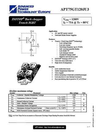
APT75GT120JU3 ISOTOP Buck chopper VCES = 1200V IC = 75A @ Tc = 80 C Trench IGBT Application C AC and DC motor control Switched Mode Power Supplies G Features Trench + Field Stop IGBT Technology - Low voltage drop E - Low tail current - Switching frequency up to 20 kHz - Soft recovery parallel diodes - Low diode VF - Low leakage current - Avalanche
9.10. Size:420K apt
apt75gn120j.pdf 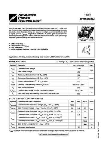
TYPICAL PERFORMANCE CURVES APT75GN120J 1200V APT75GN120J Utilizing the latest Field Stop and Trench Gate technologies, these IGBT's have ultra low VCE(ON) and are ideal for low frequency applications that require absolute minimum conduction loss. Easy paralleling is a result of very tight parameter distribution and a slightly positive VCE(ON) temperature coefficient. A built-in g
9.12. Size:606K apt
apt75gt120ju2.pdf 
APT75GT120JU2 ISOTOP Boost chopper VCES = 1200V IC = 75A @ Tc = 80 C Trench IGBT Application AC and DC motor control K Switched Mode Power Supplies Power Factor Correction Brake switch C Features Trench + Field Stop IGBT Technology G - Low voltage drop - Low tail current - Switching frequency up to 20 kHz - Soft recovery parallel diodes -
9.13. Size:331K apt
apt75gn120jdq3.pdf 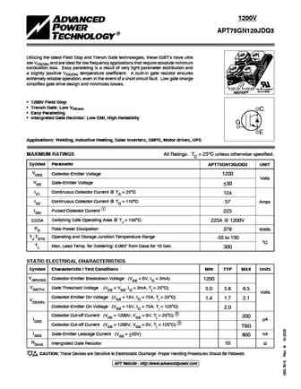
TYPICAL PERFORMANCE CURVES APT75GN120JDQ3 1200V APT75GN120JDQ3 Utilizing the latest Field Stop and Trench Gate technologies, these IGBT's have ultra low VCE(ON) and are ideal for low frequency applications that require absolute minimum conduction loss. Easy paralleling is a result of very tight parameter distribution and a slightly positive VCE(ON) temperature coefficient. A buil
9.14. Size:212K microsemi
apt75gn60bdq2g.pdf 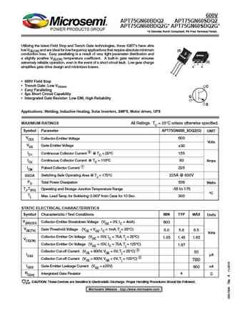
TYPICAL PERFORMANCE CURVES APT75GN60B_SDQ2(G) 600V APT75GN60BDQ2 APT75GN60SDQ2 APT75GN60BDQ2G* APT75GN60SDQ2G* *G Denotes RoHS Compliant, Pb Free Terminal Finish. Utilizing the latest Field Stop and Trench Gate technologies, these IGBT's have ultra low VCE(ON) and are ideal for low frequency applications that require absolute minimum (B) conduction loss. Easy paralleling is a result
9.15. Size:212K microsemi
apt75gn60sdq2g.pdf 
TYPICAL PERFORMANCE CURVES APT75GN60B_SDQ2(G) 600V APT75GN60BDQ2 APT75GN60SDQ2 APT75GN60BDQ2G* APT75GN60SDQ2G* *G Denotes RoHS Compliant, Pb Free Terminal Finish. Utilizing the latest Field Stop and Trench Gate technologies, these IGBT's have ultra low VCE(ON) and are ideal for low frequency applications that require absolute minimum (B) conduction loss. Easy paralleling is a result
9.16. Size:212K microsemi
apt75m50b2 apt75m50l.pdf 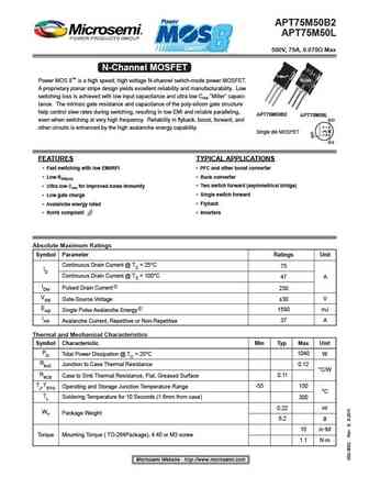
APT75M50B2 APT75M50L 500V, 75A, 0.075 Max N-Channel MOSFET T-Ma xTM TO-264 Power MOS 8 is a high speed, high voltage N-channel switch-mode power MOSFET. A proprietary planar stripe design yields excellent reliability and manufacturability. Low switching loss is achieved with low input capacitance and ultra low Crss "Miller" capaci- tance. The intrinsic gate resistance and ca
9.18. Size:268K microsemi
apt75f50b2 apt75f50l.pdf 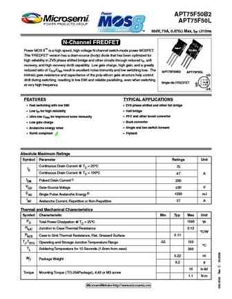
APT75F50B2 APT75F50L 500V, 75A, 0.075 Max, trr 310ns N-Channel FREDFET T-Max TO-264 Power MOS 8 is a high speed, high voltage N-channel switch-mode power MOSFET. This 'FREDFET' version has a drain-source (body) diode that has been optimized for high reliability in ZVS phase shifted bridge and other circuits through reduced trr, soft recovery, and high recovery dv/dt c
9.19. Size:254K inchange semiconductor
apt75f50l.pdf 
isc N-Channel MOSFET Transistor APT75F50L FEATURES Drain Current I = 75A@ T =25 D C Drain Source Voltage- V =500V(Min) DSS Static Drain-Source On-Resistance R =0.075 (Max) DS(on) 100% avalanche tested Minimum Lot-to-Lot variations for robust device performance and reliable operation DESCRIPTION Designed for use in switch mode power supplies and general purp
9.20. Size:375K inchange semiconductor
apt75m50b2.pdf 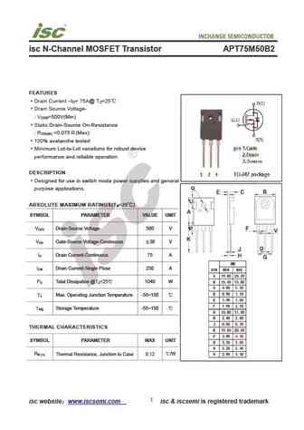
isc N-Channel MOSFET Transistor APT75M50B2 FEATURES Drain Current I = 75A@ T =25 D C Drain Source Voltage- V =500V(Min) DSS Static Drain-Source On-Resistance R =0.075 (Max) DS(on) 100% avalanche tested Minimum Lot-to-Lot variations for robust device performance and reliable operation DESCRIPTION Designed for use in switch mode power supplies and general pur
9.21. Size:254K inchange semiconductor
apt75m50l.pdf 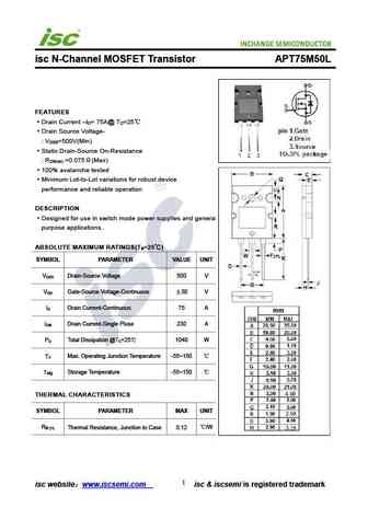
isc N-Channel MOSFET Transistor APT75M50L FEATURES Drain Current I = 75A@ T =25 D C Drain Source Voltage- V =500V(Min) DSS Static Drain-Source On-Resistance R =0.075 (Max) DS(on) 100% avalanche tested Minimum Lot-to-Lot variations for robust device performance and reliable operation DESCRIPTION Designed for use in switch mode power supplies and general purp
9.22. Size:375K inchange semiconductor
apt75f50b2.pdf 
isc N-Channel MOSFET Transistor APT75F50B2 FEATURES Drain Current I = 75A@ T =25 D C Drain Source Voltage- V =500V(Min) DSS Static Drain-Source On-Resistance R =0.075 (Max) DS(on) 100% avalanche tested Minimum Lot-to-Lot variations for robust device performance and reliable operation DESCRIPTION Designed for use in switch mode power supplies and general pur
Другие IGBT... APT60N90JC3, APT66F60B2, APT66F60L, APT66M60B2, APT66M60L, APT6M100K, APT7575AN, APT7575BN, AON6426, APT7590BN, APT75F50B2, APT75F50L, APT75M50B2, APT75M50L, APT77N60BC6, APT77N60SC6, APT7F100B