IPB029N06N3 datasheet, аналоги, основные параметры
Наименование производителя: IPB029N06N3
Тип транзистора: MOSFET
Полярность: N
Предельные значения
Pd ⓘ
- Максимальная рассеиваемая мощность: 188 W
|Vds|ⓘ - Максимально допустимое напряжение сток-исток: 60 V
|Vgs|ⓘ - Максимально допустимое напряжение затвор-исток: 20 V
|Id| ⓘ - Максимально допустимый постоянный ток стока: 120 A
Tj ⓘ - Максимальная температура канала: 175 °C
Электрические характеристики
tr ⓘ -
Время нарастания: 120 ns
Cossⓘ - Выходная емкость: 2200 pf
RDSonⓘ - Сопротивление сток-исток открытого транзистора: 0.0032 Ohm
Тип корпуса: D2PAK
TO-263
Аналог (замена) для IPB029N06N3
- подборⓘ MOSFET транзистора по параметрам
IPB029N06N3 даташит
..1. Size:258K inchange semiconductor
ipb029n06n3.pdf 
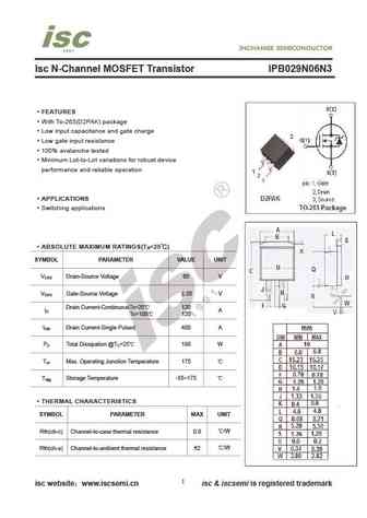
Isc N-Channel MOSFET Transistor IPB029N06N3 FEATURES With To-263(D2PAK) package Low input capacitance and gate charge Low gate input resistance 100% avalanche tested Minimum Lot-to-Lot variations for robust device performance and reliable operation APPLICATIONS Switching applications ABSOLUTE MAXIMUM RATINGS(T =25 ) a SYMBOL PARAMETER VALUE UNIT V Drain-Source V
0.1. Size:996K infineon
ipb029n06n3ge8187.pdf 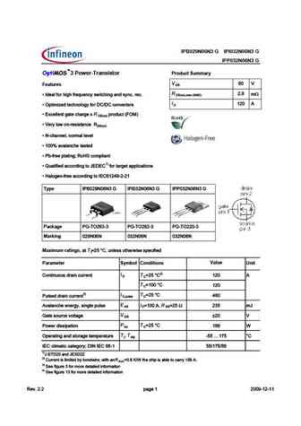
pe IPB029N06N3 G IPI032N06N3 G IPP032N06N3 G 3 Power-Transistor Product Summary V Features D R m Q #4513I CG9D389>7 1>4 CI>3 B53 , ?> =1H ,& I 1 Q ( @D9=9J54 D538>?F5BD5BC D Q H35
0.2. Size:483K infineon
ipb029n06n3g ipi032n06n3g ipp032n06n3g.pdf 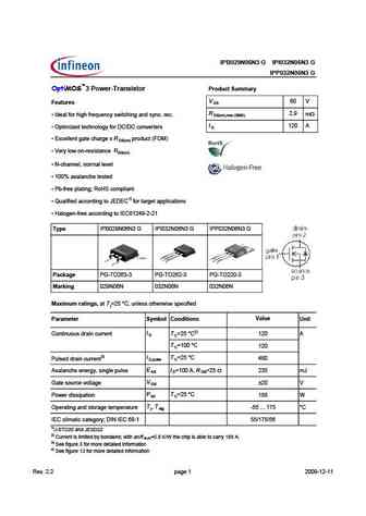
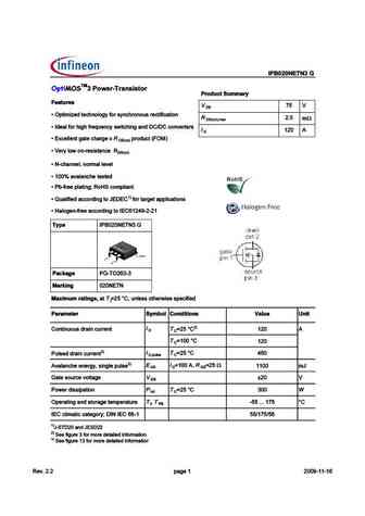
Type IPB029N06N3 G IPI032N06N3 G IPP032N06N3 G OptiMOS 3 Power-Transistor Product Summary V 60 V Features DS R 2.9 m Ideal for high frequency switching and sync. rec. DS(on),max (SMD) I 120 A Optimized technology for DC/DC converters D Excellent gate charge x R product (FOM) DS(on) Very low on-resistance RDS(on) N-channel, normal level 100% avalanche t
9.3. Size:841K infineon
ipb025n08n3g.pdf 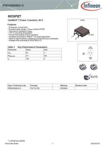
IPB025N08N3 G MOSFET D PAK OptiMOS 3 Power-Transistor, 80 V Features N-channel, normal level Excellent gate charge x R product (FOM) DS(on) Very low on-resistance R DS(on) 175 C operating temperature Pb-free lead plating; RoHS compliant Qualified according to JEDEC1) for target application Ideal for high-frequency switching and synchronous rectificat
9.4. Size:999K infineon
ipp024n06n3g ipb021n06n3g ipi024n06n3g.pdf 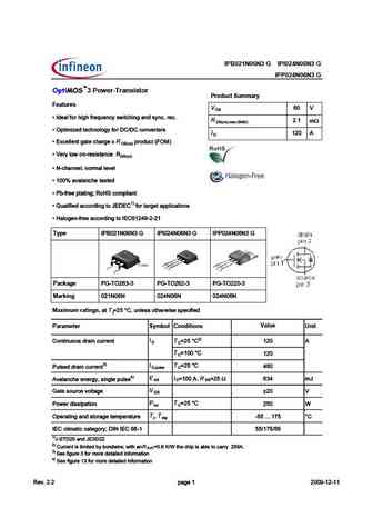
pe IPB021N06N3 G IPI024N06N3 G IPP024N06N3 G 3 Power-Transistor Product Summary Features V D Q #4513I CG9D389>7 1>4 CI>3 B53 R 1 m , ?> =1H ,& Q ( @D9=9J54 D538>?F5BD5BC I 1 D Q H35
9.6. Size:583K infineon
ipb023n04n ipp023n04ng ipb023n04ng.pdf 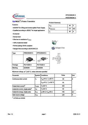
pe IPP023N04N G IPB023N04N G 3 Power-Transistor Product Summary Features V 4 D Q &( , - 7@B ( + ?8 2?5 . ? ?D6BBEAD 3=6 )@G6B ,EAA=I R m , @? >2H 1) Q * E2= 7 65 244@B5 ?8 D@ $ 7@B D2B86D 2AA= 42D @?C I D Q ' 492??6= Q '@B>2= =6F6= Q . =DB2 =@G @? B6C CD2?46 R D n) Q F2=2?496 D6CD65 Q )3 7B66 A=2D ?8 + @", 4@>A= 2?D Q "2=@86? 7B66 244@B5 ?8 D@ # Type #) ' '
9.7. Size:1134K infineon
ipb027n10n5.pdf 
MOSFET Metal Oxide Semiconductor Field Effect Transistor OptiMOSTM OptiMOS 5 Power-Transistor, 100 V IPB027N10N5 Data Sheet Rev. 2.1 Final Power Management & Multimarket OptiMOS 5 Power-Transistor, 100 V IPB027N10N5 D PAK 1 Description Features Ideal for high frequency switching and sync. rec. Excellent gate charge x R product (FOM) DS(on) Very low on-resista
9.8. Size:553K infineon
ipb025n08n3.pdf 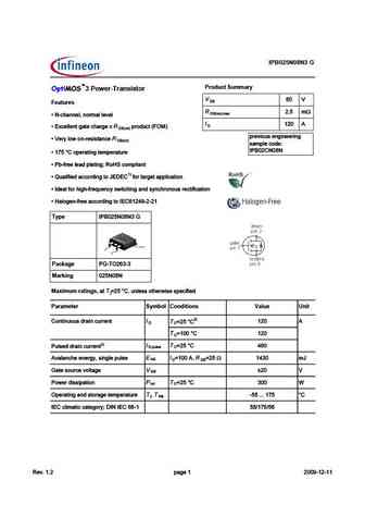
IPB025N08N3 G Product Summary 3 Power-Transistor V 80 V DS Features R 2.5 m DS(on) max Q ' 381>>5?B=1
9.9. Size:531K infineon
ipb027n10n3g.pdf 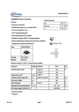
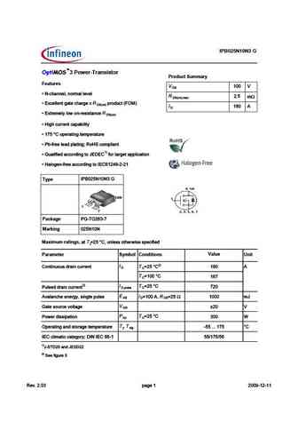
IPB027N10N3 G 3 Power-Transistor Product Summary Features V 1 D Q ' 381>>5?B=1
9.10. Size:483K infineon
ipb021n06n3g ipi024n06n3g ipp024n06n3g.pdf 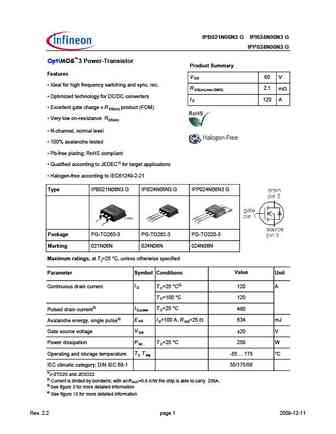
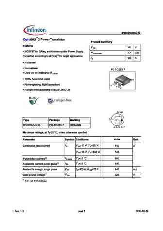
Type IPB021N06N3 G IPI024N06N3 G IPP024N06N3 G OptiMOS 3 Power-Transistor Product Summary Features V 60 V DS Ideal for high frequency switching and sync. rec. R 2.1 m DS(on),max (SMD) Optimized technology for DC/DC converters I 120 A D Excellent gate charge x R product (FOM) DS(on) Very low on-resistance RDS(on) N-channel, normal level 100% avalanch
9.11. Size:1011K infineon
ipb020n10n5lf.pdf 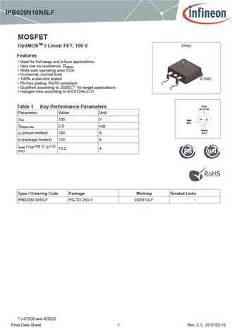
IPB020N10N5LF MOSFET D PAK OptiMOSTM 5 Linear FET, 100 V Features Ideal for hot-swap and e-fuse applications Very low on-resistance R DS(on) Wide safe operating area SOA N-channel, normal level 100% avalanche tested Pb-free plating; RoHS compliant Qualified according to JEDEC1) for target applications Halogen-free according to IEC61249-2-21 Drain
9.12. Size:671K infineon
ipb023n06n3.pdf 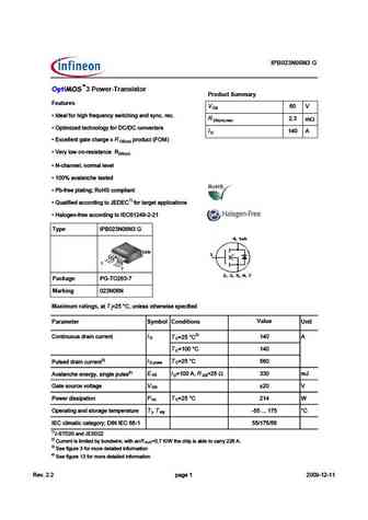
pe IPB023N06N3 G 3 Power-Transistor Product Summary Features V D Q #4513I CG9D389>7 1>4 CI>3 B53 R m D n) m x Q ( @D9=9J54 D538>?F5BD5BC I 14 D Q H35
9.13. Size:1169K infineon
ipb020n10n5.pdf 
MOSFET Metal Oxide Semiconductor Field Effect Transistor OptiMOSTM OptiMOS 5 Power-Transistor, 100 V IPB020N10N5 Data Sheet Rev. 2.1 Final Power Management & Multimarket OptiMOS 5 Power-Transistor, 100 V IPB020N10N5 D PAK 1 Description Features N-channel, normal level Optimized for FOM OSS Very low on-resistance R DS(on) 175 C operating temperature
9.14. Size:680K infineon
ipb022n04l.pdf 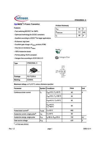
Type IPB022N04L G 3 Power-Transistor Product Summary Features V 40 V DS Fast switching MOSFET for SMPS R 2.2 mW DS(on),max Optimized technology for DC/DC converters I 90 A D Qualified according to JEDEC1) for target applications N-channel, logic level Excellent gate charge x R product (FOM) DS(on) Very low on-resistance R DS(on) 100% Avalanc
9.15. Size:1126K infineon
ipb024n08n5.pdf 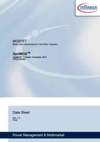
MOSFET Metal Oxide Semiconductor Field Effect Transistor OptiMOSTM OptiMOS 5 Power-Transistor, 80 V IPB024N08N5 Data Sheet Rev. 2.0 Final Power Management & Multimarket OptiMOS 5 Power-Transistor, 80 V IPB024N08N5 D PAK 1 Description Features Ideal for high frequency switching and sync. rec. Excellent gate charge x R product (FOM) DS(on) Very low on-resistance
9.16. Size:245K infineon
ipp023n04n-g ipb023n04n-g.pdf 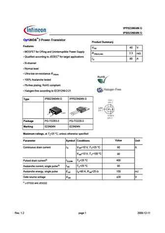
Type IPP023N04N G IPB023N04N G OptiMOS 3 Power-Transistor Product Summary Features V 40 V DS MOSFET for ORing and Uninterruptible Power Supply R 2.3 m DS(on),max Qualified according to JEDEC1) for target applications I 90 A D N-channel Normal level Ultra-low on-resistance R DS(on) 100% Avalanche tested Pb-free plating; RoHS compliant Hal
9.17. Size:1131K infineon
ipb020n08n5.pdf 
MOSFET Metal Oxide Semiconductor Field Effect Transistor OptiMOSTM OptiMOS 5 Power-Transistor, 80 V IPB020N08N5 Data Sheet Rev. 2.0 Final Power Management & Multimarket OptiMOS 5 Power-Transistor, 80 V IPB020N08N5 D PAK 1 Description Features Ideal for high frequency switching and sync. rec. Excellent gate charge x R product (FOM) DS(on) Very low on-resistance
9.18. Size:1099K infineon
ipb024n10n5.pdf 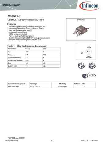
IPB024N10N5 MOSFET D -PAK 7pin OptiMOS 5 Power-Transistor, 100 V Features Ideal for high frequency switching and sync. rec. tab Excellent gate charge x R product (FOM) DS(on) Very low on-resistance R DS(on) N-channel, normal level 1 100% avalanche tested Pb-free plating; RoHS compliant 7 Qualified according to JEDEC1) for target applications H
9.19. Size:563K infineon
ipb026n06n.pdf 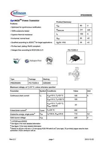
Type IPB026N06N OptiMOSTM Power-Transistor Product Summary Features VDS 60 V Optimized for synchronous rectification RDS(on),max 2.6 mW 100% avalanche tested ID 100 A Superior thermal resistance Qoss 65 nC N-channel, normal level Qualified according to JEDEC1) for target applications Qg(0V..10V) 56 nC Pb-free lead plating; RoHS compliant Haloge
9.20. Size:258K inchange semiconductor
ipb027n10n5.pdf 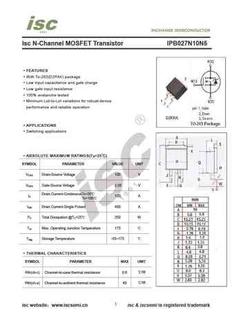
Isc N-Channel MOSFET Transistor IPB027N10N5 FEATURES With To-263(D2PAK) package Low input capacitance and gate charge Low gate input resistance 100% avalanche tested Minimum Lot-to-Lot variations for robust device performance and reliable operation APPLICATIONS Switching applications ABSOLUTE MAXIMUM RATINGS(T =25 ) a SYMBOL PARAMETER VALUE UNIT V Drain-Source V
9.21. Size:258K inchange semiconductor
ipb020n10n5lf.pdf 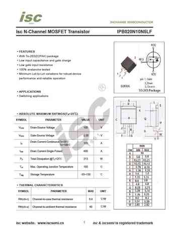
Isc N-Channel MOSFET Transistor IPB020N10N5LF FEATURES With To-263(D2PAK) package Low input capacitance and gate charge Low gate input resistance 100% avalanche tested Minimum Lot-to-Lot variations for robust device performance and reliable operation APPLICATIONS Switching applications ABSOLUTE MAXIMUM RATINGS(T =25 ) a SYMBOL PARAMETER VALUE UNIT V Drain-Source
9.22. Size:228K inchange semiconductor
ipb021n06n3g.pdf 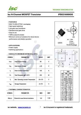
Isc N-Channel MOSFET Transistor IPB021N06N3G FEATURES With TO-263( D PAK ) packaging High speed switching Low gate input resistance Standard level gate drive Easy to use 100% avalanche tested Minimum Lot-to-Lot variations for robust device performance and reliable operation APPLICATIONS Power supply Switching applications ABSOLUTE MAXIMUM RATINGS(T =25 )
9.23. Size:258K inchange semiconductor
ipb027n10n3.pdf 
Isc N-Channel MOSFET Transistor IPB027N10N3 FEATURES With To-263(D2PAK) package Low input capacitance and gate charge Low gate input resistance 100% avalanche tested Minimum Lot-to-Lot variations for robust device performance and reliable operation APPLICATIONS Switching applications ABSOLUTE MAXIMUM RATINGS(T =25 ) a SYMBOL PARAMETER VALUE UNIT V Drain-Source V
9.24. Size:258K inchange semiconductor
ipb023n04n.pdf 
isc N-Channel MOSFET Transistor IPB023N04N FEATURES With TO-263( D2PAK ) packaging High speed switching Low gate input resistance Standard level gate drive Easy to use 100% avalanche tested Minimum Lot-to-Lot variations for robust device performance and reliable operation APPLICATIONS Power supply Switching applications ABSOLUTE MAXIMUM RATINGS(T =25 ) a
9.25. Size:204K inchange semiconductor
ipb020n10n5.pdf 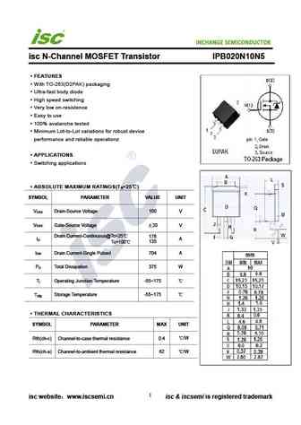
INCHANGE Semiconductor isc N-Channel MOSFET Transistor IPB020N10N5 FEATURES With TO-263(D2PAK) packaging Ultra-fast body diode High speed switching Very low on-resistence Easy to use 100% avalanche tested Minimum Lot-to-Lot variations for robust device performance and reliable operationz APPLICATIONS Switching applications ABSOLUTE MAXIMUM RATINGS(T =25 ) a
9.26. Size:257K inchange semiconductor
ipb026n06n.pdf 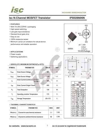
isc N-Channel MOSFET Transistor IPB026N06N FEATURES With TO-263( D2PAK ) packaging High speed switching Low gate input resistance Standard level gate drive Easy to use 100% avalanche tested Minimum Lot-to-Lot variations for robust device performance and reliable operation APPLICATIONS Power supply Switching applications ABSOLUTE MAXIMUM RATINGS(T =25 ) a
Другие IGBT... IPF075N03L, FQB70N08, FTP03N03N, IPB015N04N, IPB019N06L3, IPB020N10N5LF, IPB023N04N, IPB027N10N3, AON7403, IPB031NE7N3, IPB033N10N5LF, IPB037N06N3, IPB039N04L, IPB041N04N, IPB049N06L3, IPB049NE7N3, IPB054N06N3