2305. Аналоги и основные параметры
Наименование производителя: 2305
Тип транзистора: MOSFET
Полярность: P
Предельные значения
Pd ⓘ - Максимальная рассеиваемая мощность: 0.35 W
|Vds|ⓘ - Максимально допустимое напряжение сток-исток: 8 V
|Vgs|ⓘ - Максимально допустимое напряжение затвор-исток: 8 V
|Id| ⓘ - Максимально допустимый постоянный ток стока: 4.1 A
Tj ⓘ - Максимальная температура канала: 150 °C
Электрические характеристики
tr ⓘ - Время нарастания: 35 ns
Cossⓘ - Выходная емкость: 290 pf
RDSonⓘ - Сопротивление сток-исток открытого транзистора: 0.045 Ohm
Тип корпуса: SOT-23
Аналог (замена) для 2305
- подборⓘ MOSFET транзистора по параметрам
2305 даташит
2305.pdf
2305 MOSFET(P-Channel) V(BR)DSS RDS(ON)MAX ID SOT-23 45m @-4.5V SOT-23 Plastic-Encapsulate MOSFET -12V 60m @-2.5V -4.1A 90m @-1.8V Features SOT-23 TrenchFET Power MOSFET Load Switch for Portable Devices. DC/DC Converter. Mechanical Data SOT-23 SOT-23 Small Outline Plastic Package. UL
rn2301 rn2302 rn2303 rn2304 rn2305 rn2306.pdf
RN2301 RN2306 TOSHIBA Transistor Silicon PNP Epitaxial Type (PCT Process) RN2301,RN2302,RN2303 RN2304,RN2305,RN2306 Unit mm Switching, Inverter Circuit, Interface Circuit and Driver Circuit Applications With built-in bias resistors Simplify circuit design Reduce a quantity of parts and manufacturing process Complementary to RN1301to1306 Equivalent Circuit Bias Resi
rej03g0026 h5n2305pf.pdf
To our customers, Old Company Name in Catalogs and Other Documents On April 1st, 2010, NEC Electronics Corporation merged with Renesas Technology Corporation, and Renesas Electronics Corporation took over all the business of both companies. Therefore, although the old company name remains in this document, it is a valid Renesas Electronics document. We appreciate your understanding.
si2305ad.pdf

New Product Si2305ADS Vishay Siliconix P-Channel 8-V (D-S) MOSFET FEATURES PRODUCT SUMMARY Halogen-free According to IEC 61249-2-21 VDS (V) RDS(on) ( )ID (A) Qg (Typ.) Definition 0.040 at VGS = - 4.5 V - 4.1 TrenchFET Power MOSFET - 8 0.060 at VGS = - 2.5 V - 3.4 7.8 nC 100 % Rg Tested 0.088 at VGS = - 1.8 V - 2.0 APPLICATIONS Load Switch DC/DC Conv
si2305cds.pdf

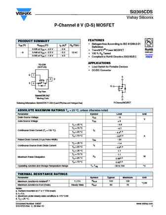
Si2305CDS Vishay Siliconix P-Channel 8 V (D-S) MOSFET FEATURES PRODUCT SUMMARY Halogen-free According to IEC 61249-2-21 VDS (V) RDS(on) ( ) ID (A)d Qg (Typ.) Definition 0.035 at VGS = - 4.5 V - 5.8 TrenchFET Power MOSFET - 8 0.048 at VGS = - 2.5 V - 5.0 12 nC 100 % Rg Tested 0.065 at VGS = - 1.8 V - 4.3 Compliant to RoHS Directive 2002/95/EC APPLICATIONS
si2305cd.pdf
Si2305CDS Vishay Siliconix P-Channel 8 V (D-S) MOSFET FEATURES PRODUCT SUMMARY Halogen-free According to IEC 61249-2-21 VDS (V) RDS(on) ( ) ID (A)d Qg (Typ.) Definition 0.035 at VGS = - 4.5 V - 5.8 TrenchFET Power MOSFET - 8 0.048 at VGS = - 2.5 V - 5.0 12 nC 100 % Rg Tested 0.065 at VGS = - 1.8 V - 4.3 Compliant to RoHS Directive 2002/95/EC APPLICATIONS
si2305ads.pdf
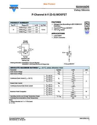
New Product Si2305ADS Vishay Siliconix P-Channel 8-V (D-S) MOSFET FEATURES PRODUCT SUMMARY Halogen-free According to IEC 61249-2-21 VDS (V) RDS(on) ( )ID (A) Qg (Typ.) Definition 0.040 at VGS = - 4.5 V - 4.1 TrenchFET Power MOSFET - 8 0.060 at VGS = - 2.5 V - 3.4 7.8 nC 100 % Rg Tested 0.088 at VGS = - 1.8 V - 2.0 APPLICATIONS Load Switch DC/DC Conv
si2305ds.pdf
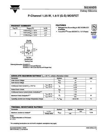
Si2305DS Vishay Siliconix P-Channel 1.25-W, 1.8-V (G-S) MOSFET FEATURES PRODUCT SUMMARY Halogen-free According to IEC 61249-2-21 VDS (V) RDS(on) ( )ID (A) Available 0.052 at VGS = - 4.5 V 3.5 TrenchFET Power MOSFETs 1.8 V Rated 0.071 at VGS = - 2.5 V - 8 3 0.108 at VGS = - 1.8 V 2 TO-236 (SOT-23) G 1 3 D S 2 Top View Si2305DS (A5)* * Mark
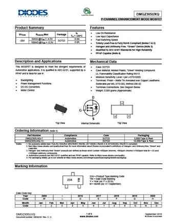
dmp2305uvt.pdf
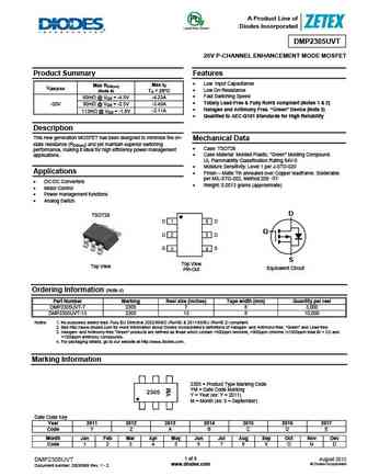
A Product Line of Diodes Incorporated DMP2305UVT 20V P-CHANNEL ENHANCEMENT MODE MOSFET Product Summary Features Low Input Capacitance Max ID Max RDS(on) V(BR)DSS Low On-Resistance (Note 6) TA = 25 C Fast Switching Speed 60m @ VGS = -4.5V -4.23A Totally Lead-Free & Fully RoHS compliant (Notes 1 & 2) -20V 90m @ VGS = -2.5V -3.49A Halogen and Ant
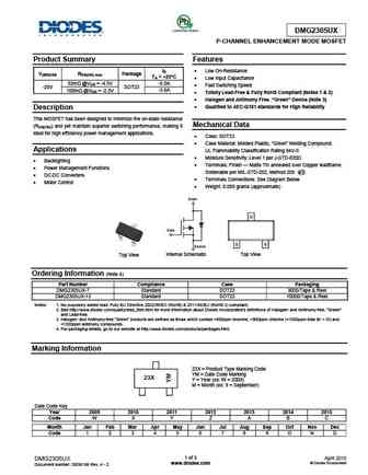
dmg2305uxq.pdf
DMG2305UXQ P-CHANNEL ENHANCEMENT MODE MOSFET Product Summary Features ID Low On-Resistance BVDSS RDS(ON) Max Package TA = +25 C Low Input Capacitance 52m @VGS = -4.5V -5.0A Fast Switching Speed -20V SOT23 -3.6A 100m @VGS = -2.5V Totally Lead-Free & Fully RoHS Compliant (Notes 1 & 2) Halogen and Antimony Free. Green Device (Note 3)
dmp2305u.pdf
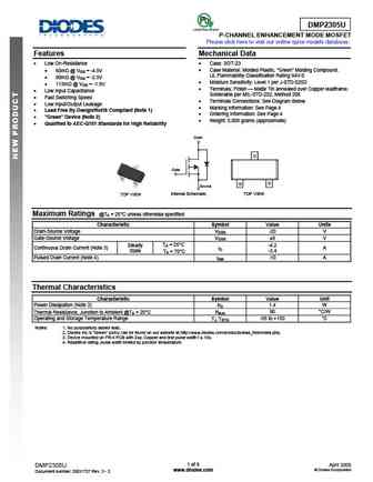
DMP2305U P-CHANNEL ENHANCEMENT MODE MOSFET Please click here to visit our online spice models database. Features Mechanical Data Low On-Resistance Case SOT-23 60m @ VGS = -4.5V Case Material Molded Plastic, Green Molding Compound. UL Flammability Classification Rating 94V-0 90m @ VGS = -2.5V Moisture Sensitivity Level 1 per J-STD-020D 11
mcs2305b.pdf
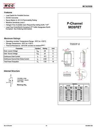
MCS2305B Features Load Switch for Portable Devices DC/DC Converter Epoxy Meets UL 94 V-0 Flammability Rating Moisture Sensitivity Level 1 P-Channel Halogen Free Available Upon Request By Adding Suffix "-HF" Lead Free Finish/RoHS Compliant ("P" Suffix Designates RoHS MOSFET Compliant. See Ordering Information) Maximum Ratings Operating Junction Temperature
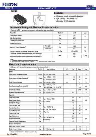
si2305b.pdf
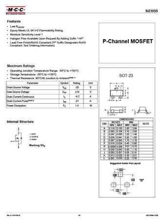
SI2305B Features Low RDS(ON) Epoxy Meets UL 94 V-0 Flammability Rating Moisture Sensitivity Level 1 Halogen Free Available Upon Request By Adding Suffix "-HF" P-Channel MOSFET Lead Free Finish/RoHS Compliant ("P" Suffix Designates RoHS Compliant. See Ordering Information) Maximum Ratings Operating Junction Temperature Range -55 C to +150 C Storage Tempe
ut2305a.pdf
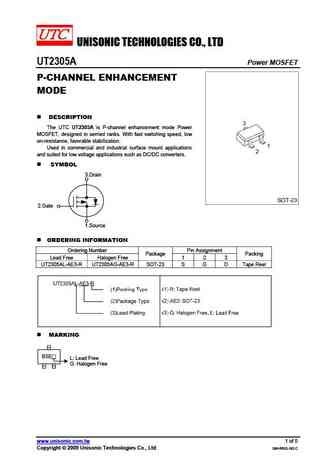
UNISONIC TECHNOLOGIES CO., LTD UT2305A Power MOSFET P-CHANNEL ENHANCEMENT MODE DESCRIPTION The UTC UT2305A is P-channel enhancement mode Power MOSFET, designed in serried ranks. With fast switching speed, low on-resistance, favorable stabilization. Used in commercial and industrial surface mount applications and suited for low voltage applications such as DC/DC converters.
ut2305l-ae2-r ut2305g-ae2-r ut2305l-ae3-r ut2305g-ae3-r ut2305l-al3-r ut2305g-ag3-r.pdf
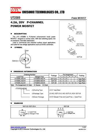
UNISONIC TECHNOLOGIES CO., LTD UT2305 Power MOSFET 4.2A, 20V P-CHANNEL POWER MOSFET DESCRIPTION The UTC UT2305 is P-channel enhancement mode power MOSFET, designed in serried ranks. With fast switching speed, low on-resistance, favorable stabilization. Used in commercial and industrial surface mount applications and suited for low voltage applications such as DC/DC conve
ut2305.pdf
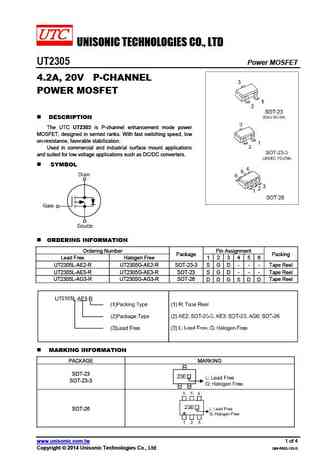
UNISONIC TECHNOLOGIES CO., LTD UT2305 Power MOSFET 4.2A, 20V P-CHANNEL POWER MOSFET DESCRIPTION The UTC UT2305 is P-channel enhancement mode power MOSFET, designed in serried ranks. With fast switching speed, low on-resistance, favorable stabilization. Used in commercial and industrial surface mount applications and suited for low voltage applications such as DC/DC conve
ut2305g-ae2-r ut2305g-ae3-r ut2305g-ag3-r.pdf
UNISONIC TECHNOLOGIES CO., LTD UT2305 Power MOSFET 4.2A, 20V P-CHANNEL POWER MOSFET DESCRIPTION The UTC UT2305 is P-channel enhancement mode power MOSFET, designed in serried ranks. With fast switching speed, low on-resistance, favorable stabilization. Used in commercial and industrial surface mount applications and suited for low voltage applications such as DC/DC conve
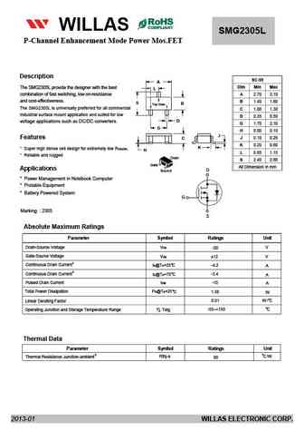
smg2305.pdf
SMG2305 -4.2A, -20V,RDS(ON) 65m Elektronische Bauelemente P-Channel Enhancement Mode Power Mos.FET RoHS Compliant Product A suffix of -C specifies halogen & lead-free Description SC-59 A Dim Min Max The SMG2305 provide the designer with the best L combination of fast switching, low on-resistance A 2.70 3.10 3 and cost-effectiveness. B 1.40 1.60 S B Top View 2 1
smg2305p.pdf
SMG2305P -4.5A , -20V , RDS(ON) 43 m P-Channel Enhancement MOSFET Elektronische Bauelemente RoHS Compliant Product A suffix of -C specifies halogen & lead-free DESCRIPTION SC-59 These miniature surface mount MOSFETs utilize a high A cell density trench process to provide low RDS(on) and to L ensure minimal power loss and heat dissipation. 3 3 Top
smg2305pe.pdf
SMG2305PE -4.5 A, -20 V, RDS(ON) 43 m P-Channel Enhancement MOSFET Elektronische Bauelemente RoHS Compliant Product A suffix of -C specifies halogen & lead-free DESCRIPTION SC-59 These miniature surface mount MOSFETs utilize a high cell density trench process to provide low RDS(on) and to A L ensure minimal power loss and heat dissipation. Typical 3 3 applicat
sgm2305a.pdf
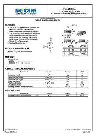
SGM2305A -3.2 A, -30 V, RDS(ON) 80 m P-Channel Enhancement Mode Power MOSFET Elektronische Bauelemente RoHS Compliant Product A suffix of -C specifies halogen & lead-free SOT-89 FEATURES A The SGM2305A provide the designer with best combination of fast switching, 4 Top View C B low on-resistance and cost-effectiveness. The SGM2305A is universally preferred
tsm2305cx.pdf
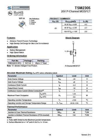
TSM2305 20V P-Channel MOSFET SOT-23 PRODUCT SUMMARY Pin Definition 1. Gate VDS (V) RDS(on)(m ) ID (A) 2. Source 3. Drain 55 @ VGS =-4.5V -3.2 80 @ VGS =-2.5V -2.7 -20 130 @ VGS =-1.8V -2.0 Block Diagram Features Advance Trench Process Technology High Density Cell Design for Ultra Low On-resistance Application Battery Management High Spe
cjk2305.pdf
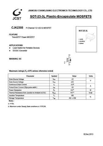
JIANGSU CHANGJIANG ELECTRONICS TECHNOLOGY CO., LTD SOT-23-3L Plastic-Encapsulate MOSFETS CJK2305 P-Channel 12-V(D-S) MOSFET SOT-23-3L FEATURE TrenchFET Power MOSFET 1. GATE 2. SOURCE 3. DRAIN APPLICATIONS Load Switch for Portable Devices DC/DC Converter MARKING S5 Maximum ratings (Ta=25 unless otherwise noted) Parameter Symbol Value Units Drain-Source Volt
cj2305.pdf
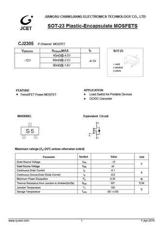
JIANGSU CHANGJIANG ELECTRONICS TECHNOLOGY CO., LTD SOT-23 Plastic-Encapsulate MOSFETS CJ2305 P-Channel MOSFET ID V(BR)DSS RDS(on)MAX SOT-23 45m @-4.5V -12V 60m @-2.5V -4.1A 1. GATE 90m @-1.8V 2. SOURCE 3. DRAIN APPLICATION FEATURE Load Switch for Portable Devices TrenchFET Power MOSFET DC/DC Converter MARKING Equivalent Circuit Maximum ratings
2sc2305.pdf
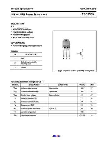
Product Specification www.jmnic.com Silicon NPN Power Transistors 2SC2305 DESCRIPTION With TO-3PN package High breakdown voltage Fast switching speed Wide safe operating area APPLICATIONS For switching regulator applications PINNING PIN DESCRIPTION 1 Base Collector;connected to 2 mounting base 3 Emitter Fig.1 simplified outline (TO-3PN) and symbol
si2305.pdf
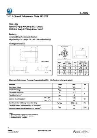
SI2305 20V P-Channel Enhancement Mode MOSFET VDS= -20V RDS(ON), Vgs@-4.5V, Ids@-2.8A 130m RDS(ON), Vgs@-2.5V, Ids@-2.0A 190m Features Advanced trench process technology High Density Cell Design For Ultra Low On-Resistance Package Dimensions D G S SOT-23(PACKAGE) Millimeter Millimeter REF. REF. Min. Max. Min. Max. A 2.70 3.10 G 1.90 REF. B 2.40 2.80 H 1.00 1.30
ceh2305.pdf
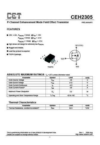
CEH2305 P-Channel Enhancement Mode Field Effect Transistor PRELIMINARY FEATURES -30V, -4.9A , RDS(ON) = 52m @VGS = -10V. RDS(ON) = 65m @VGS = -4.5V. RDS(ON) = 119m @VGS = -2.5V. High dense cell design for extremely low RDS(ON). D(1,2,5,6,) Rugged and reliable. Lead free product is acquired. TSOP-6 package. 4 5 6 G(3) 3 2 1 S(4) TSOP-6 ABSOLUTE MAXIMUM RATINGS TA
ces2305.pdf
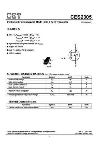
CES2305 P-Channel Enhancement Mode Field Effect Transistor PRELIMINARY FEATURES -30V, -4A, RDS(ON) = 55m @VGS = -10V. RDS(ON) = 70m @VGS = -4.5V. RDS(ON) = 120m @VGS = -2.5V. High dense cell design for extremely low RDS(ON). D Rugged and reliable. Lead-free plating ; RoHS compliant. SOT-23 package. G D S G S SOT-23 ABSOLUTE MAXIMUM RATINGS TA = 25 C unless otherwise
g2305.pdf
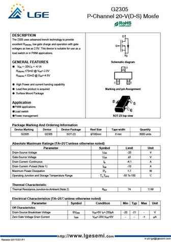
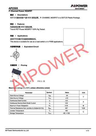
G2305 P-Channel 20-V(D-S) Mosfe DESCRIPTION D The 2305 uses advanced trench technology to provide excellent RDS(ON), low gate charge and operation with gate G voltages as low as 2.5V. This device is suitable for use as a load switch or in PWM applications. S Schematic diagram GENERAL FEATURES VDS = -20V,ID = -4.1A RDS(ON)
wtc2305ds.pdf
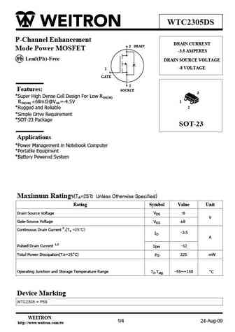
WTC2305DS P-Channel Enhancement DRAIN CURRENT 3 DRAIN Mode Power MOSFET -3.5 AMPERES DRAIN SOURCE VOLTAGE -8 VOLTAGE 1 GATE 2 Features SOURCE 3 *Super High Dense Cell Design For Low RDS(ON) 1 RDS(ON)
wtc2305.pdf
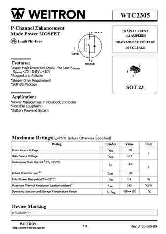
WTC2305 P-Channel Enhancement DRAIN CURRENT 3 DRAIN Mode Power MOSFET -4.2 AMPERES DRAIN SOURCE VOLTAGE -30 VOLTAGE 1 GATE 2 Features SOURCE 3 *Super High Dense Cell Design For Low RDS(ON) 1 RDS(ON)
se2305.pdf
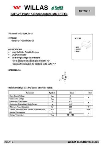
FM120-M WILLAS THRU SE2305 FM1200-M 1.0A SURFACE MOUNT SCHOTTKY SOT-23 Plastic-Encapsulate MOSFETS BARRIER RECTIFIERS -20V- 200V SOD-123 PACKAGE Pb Free Produ Package outline Features Batch process design, excellent power dissipation offers better reverse leakage current and thermal resistance. SOD-123H Low profile surface mounted application in order to optimize b
smg2305l.pdf
FM120-M WILLAS SMG2305L THRU P-Channel Enhancement Mode Power Mos.FET FM1200-M 1.0A SURFACE MOUNT SCHOTTKY BARRIER RECTIFIERS -20V- 200V SOD-123 PACKAGE Pb Free Product Package outline Features Batch process design, excellent power dissipation offers better r Descriptioneverse leakage current and thermal resistance. SOD-123H SC-59 Low profile surface mounted applic
h2305n.pdf
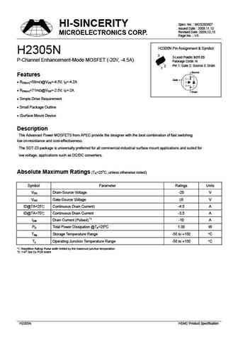
Spec. No. MOS200807 HI-SINCERITY Issued Date 2008.11.12 Revised Date 2009,12,15 MICROELECTRONICS CORP. Page No. 1/5 H2305N Pin Assignment & Symbol H2305N 3 3-Lead Plastic SOT-23 P-Channel Enhancement-Mode MOSFET (-20V, -4.5A) Package Code N Pin 1 Gate 2 Source 3 Drain 2 1 Source Features Gate RDS(on)
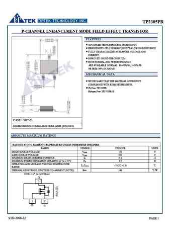
ap2305agn.pdf
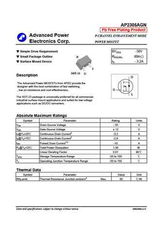
AP2305AGN Pb Free Plating Product Advanced Power P-CHANNEL ENHANCEMENT MODE Electronics Corp. POWER MOSFET Simple Drive Requirement BVDSS -30V Small Package Outline RDS(ON) 80m D Surface Mount Device ID - 3.2A S SOT-23 G Description D The Advanced Power MOSFETs from APEC provide the designer with the best combination of fast switching, G , low on-resistance and cos
ap2305cgn-hf.pdf
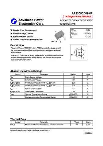
AP2305CGN-HF Halogen-Free Product Advanced Power P-CHANNEL ENHANCEMENT MODE Electronics Corp. POWER MOSFET Simple Drive Requirement BVDSS -30V D Small Package Outline RDS(ON) 85m Surface Mount Device ID - 3.2A S RoHS Compliant & Halogen-Free SOT-23 G Description D Advanced Power MOSFETs from APEC provide the designer with the best combination of fast switching,l
ap2305bgn-hf.pdf
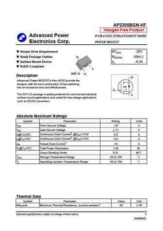
AP2305BGN-HF Halogen-Free Product Advanced Power P-CHANNEL ENHANCEMENT MODE Electronics Corp. POWER MOSFET Simple Drive Requirement BVDSS -20V Small Package Outline RDS(ON) 65m D Surface Mount Device ID -4.2A RoHS Compliant S SOT-23 G Description D Advanced Power MOSFETs from APEC provide the designer with the best combination of fast switching, low on-resistan
ap2305n-hf.pdf
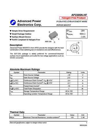
AP2305N-HF Halogen-Free Product Advanced Power P-CHANNEL ENHANCEMENT MODE Electronics Corp. POWER MOSFET Simple Drive Requirement BVDSS -20V D Small Package Outline RDS(ON) 65m Surface Mount Device ID - 3.4A S RoHS Compliant & Halogen-Free SOT-23S G D Description Advanced Power MOSFETs from APEC provide the designer with the best combination of fast switching,lo
ap2305gn-hf.pdf
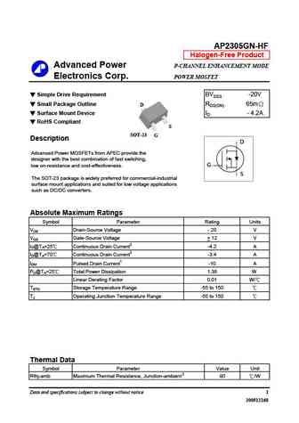
AP2305GN-HF Halogen-Free Product Advanced Power P-CHANNEL ENHANCEMENT MODE Electronics Corp. POWER MOSFET Simple Drive Requirement BVDSS -20V Small Package Outline RDS(ON) 65m D Surface Mount Device ID - 4.2A RoHS Compliant S SOT-23 G Description D Advanced Power MOSFETs from APEC provide the designer with the best combination of fast switching, G low on-resis
ap2305agn-hf.pdf
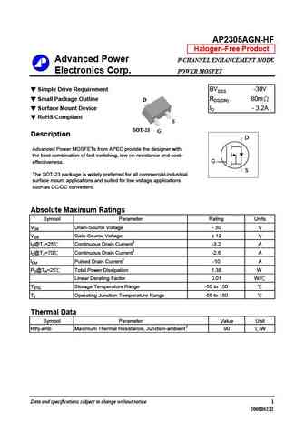
AP2305AGN-HF Halogen-Free Product Advanced Power P-CHANNEL ENHANCEMENT MODE Electronics Corp. POWER MOSFET Simple Drive Requirement BVDSS -30V Small Package Outline RDS(ON) 80m D Surface Mount Device ID - 3.2A RoHS Compliant S SOT-23 G Description D Advanced Power MOSFETs from APEC provide the designer with the best combination of fast switching, low on-resistan
am2305p.pdf
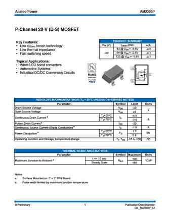
Analog Power AM2305P P-Channel 20-V (D-S) MOSFET PRODUCT SUMMARY Key Features rDS(on) (m ) VDS (V) ID(A) Low r trench technology DS(on) 43 @ VGS = -4.5V -4.5 Low thermal impedance -20 54 @ VGS = -2.5V -4.1 Fast switching speed 120 @ VGS = -1.8V -2.7 Typical Applications White LED boost converters Automotive Systems Industrial DC/DC Conversion Ci
am2305pe.pdf
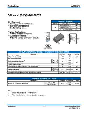
Analog Power AM2305PE P-Channel 20-V (D-S) MOSFET PRODUCT SUMMARY Key Features rDS(on) (m ) VDS (V) ID(A) Low r trench technology DS(on) 43 @ VGS = -4.5V -4.5 Low thermal impedance -20 54 @ VGS = -2.5V -4.1 Fast switching speed 120 @ VGS = -1.8V -2.7 Typical Applications White LED boost converters Automotive Systems Industrial DC/DC Conversion C
si2305b.pdf
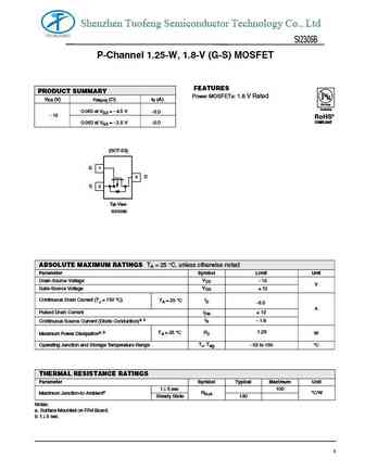
Shenzhen Tuofeng Semiconductor Technology Co., Ltd SI2305B P-Channel 1.25-W, 1.8-V (G-S) MOSFET FEATURES PRODUCT SUMMARY Power MOSFETs 1.8 V Rated VDS (V) rDS(on) ( )ID (A) Pb-free Available 0.060 at VGS = - 4.5 V -3.0 - 16 RoHS* COMPLIANT 0.080 at VGS = - 2.5 V -2.0 (SOT-23) G 1 3 D S 2 Top View Si2305B ABSOLUTE MAXIMUM RATINGS TA = 25 C, unless otherwise noted Para
mtp2305n3.pdf
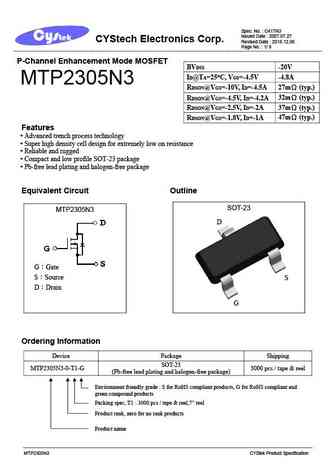
Spec. No. C417N3 Issued Date 2007.07.27 CYStech Electronics Corp. Revised Date 2018.12.06 Page No. 1/ 9 P-Channel Enhancement Mode MOSFET BVDSS -20V ID@TA=25 C, VGS=-4.5V -4.8A MTP2305N3 27m (typ.) RDSON@VGS=-10V, ID=-4.5A 32m (typ.) RDSON@VGS=-4.5V, ID=-4.2A 37m (typ.) RDSON@VGS=-2.5V, ID=-2A 47m (typ.) RDSON@VGS=-1.8V, ID=-1A Features
g2305.pdf
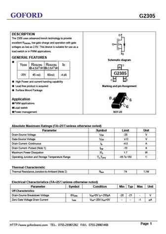
GOFORD G2305 DESCRIPTION D The 2305 uses advanced trench technology to provide excellent RDS(ON), low gate charge and operation with gate G voltages as low as 2.5V. This device is suitable for use as a load switch or in PWM applications. S GENERAL FEATURES Schematic diagram VDSS RDS(ON) RDS(ON) ID (Typ) @-2.5V @-4.5V (Typ) G2305 -20V 45 m 60m -4.8 A
sts2305a.pdf
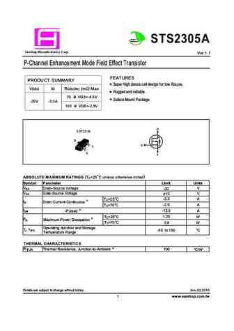
Green Product STS2305A a S mHop Microelectronics C orp. Ver 1.1 P-Channel Enhancement Mode Field Effect Transistor FEATURES PRODUCT SUMMARY Super high dense cell design for low RDS(ON). VDSS ID RDS(ON) (m ) Max Rugged and reliable. 70 @ VGS=-4.5V Suface Mount Package. -20V -3.3A 100 @ VGS=-2.5V D S OT23-3L D G S G S (TC=25 C unless otherwise noted) ABSOLUTE MAXIMUM RA
sts2305.pdf
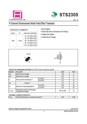
Green Product STS2305 a S mHop Microelectronics C orp. Ver 1.0 P-Channel Enhancement Mode Field Effect Transistor FEATURES PRODUCT SUMMARY Super high dense cell design for low RDS(ON). VDSS ID RDS(ON) (m ) Max Rugged and reliable. 57 @ VGS=-4.5V Suface Mount Package. 78 @ VGS=-4.0V 83 @ VGS=-3.7V -20V -3.4A 93 @ VGS=-3.1V 115 @ VGS=-2.5V D SOT-23 D G S G S ABSOL
ssf2305.pdf
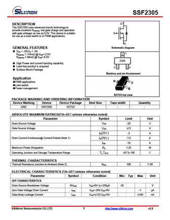
SSF2305 D DESCRIPTION The SSF2305 uses advanced trench technology to provide excellent RDS(ON), low gate charge and operation with gate voltages as low as 0.5V. This device is suitable G for use as a load switch or in PWM applications. S Schematic diagram GENERAL FEATURES VDS = -20V,ID = -3A RDS(ON)
brcs2305mc.pdf
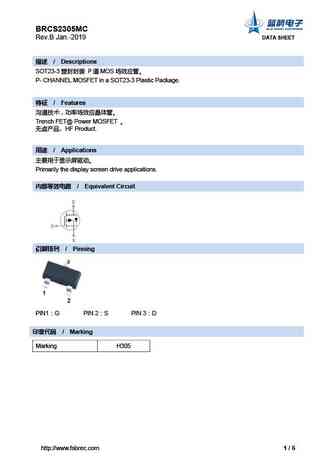
BRCS2305MC Rev.B Jan.-2019 DATA SHEET / Descriptions SOT23-3 P MOS P- CHANNEL MOSFET in a SOT23-3 Plastic Package. / Features Trench FET@ Power MOSFET HF Product. / Applications Primarily the display screen drive applications.
lp2305dslt1g s-lp2305dslt1g.pdf
LESHAN RADIO COMPANY, LTD. 12V P-Channel Enhancement-Mode MOSFET LP2305DSLT1G V = -12V DS S-LP2305DSLT1G RDS(ON), Vgs@-4.5V, Ids@" 3.5A = 68m R 3A = 81 DS(ON), Vgs@-2.5V, Ids@" m R 2A = 118 m DS(ON), Vgs@-1.8V, Ids@" 3 Features Advanced trench process technology 1 High Density Cell Design For Ultra Low On-Resistance 2 SOT 23 (TO 236AB) Fully Characterized Avalan
lp2305dslt1g.pdf
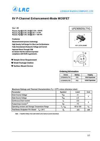
LESHAN RADIO COMPANY, LTD. 8V P-Channel Enhancement-Mode MOSFET V = -8V DS LP2305DSLT1G RDS(ON), Vgs@-4.5V, Ids@" 3.5A = 58m R 3A = 71 DS(ON), Vgs@-2.5V, Ids@" m R 2A = 108 m DS(ON), Vgs@-1.8V, Ids@" 3 Features 1 Advanced trench process technology 2 High Density Cell Design For Ultra Low On-Resistance SOT 23 (TO 236AB) Fully Characterized Avalanche Voltage and
sm2305psa.pdf
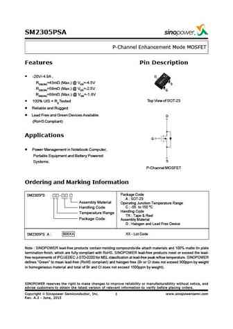
SM2305PSA P-Channel Enhancement Mode MOSFET Features Pin Description -20V/-4.9A , D RDS(ON)=43m (Max.) @ VGS=-4.5V S RDS(ON)=58m (Max.) @ VGS=-2.5V G RDS(ON)=88m (Max.) @ VGS=-1.8V Top View of SOT-23 100% UIS + Rg Tested Reliable and Rugged Lead Free and Green Devices Available D (RoHS Compliant) Applications G Power Management in Notebook Computer, Po
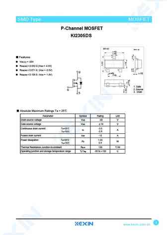
ki2305.pdf
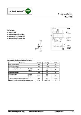
SMD Type MOSFET Product specification KI2305 SOT-23-3 Unit mm 2.9+0.2 -0.2 Features 0.4+0.1 -0.05 3 VDS (V) = -20V RDS(ON) 0.065 (VGS = -4.5V) RDS(ON) 0.100 (VGS = -2.5V) 12 RDS(ON) 0.250 (VGS = -1.8V) +0.1 0.95-0.1 0.1+0.05 -0.01 +0.2 1.9-0.2 D 1. Gate 2. Source 3. Drain G S Absolute Maximum Ratings Ta = 25 Parameter Sym
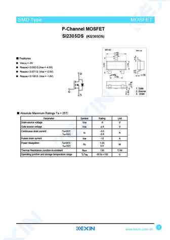
si2305ds-3.pdf
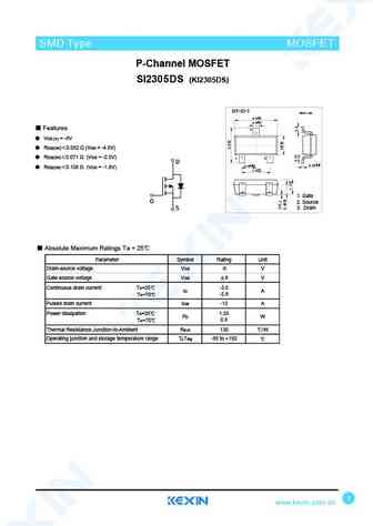
SMD Type MOSFET SMD Type P-Channel MOSFET SI2305DS (KI2305DS) SOT-23-3 Unit mm +0.2 2.9-0.1 +0.1 0.4 -0.1 Features 3 VDS (V) = -8V RDS(ON) 0.052 (VGS = -4.5V) RDS(ON) 0.071 (VGS = -2.5V) 1 2 D +0.02 +0.1 0.15 -0.02 0.95 -0.1 RDS(ON) 0.108 (VGS = -1.8V) +0.1 1.9-0.2 1. Gate G 2. Source 3. Drain S Absolute Maximum Ratings Ta
ki2305ds.pdf
SMD Type MOSFET SMD Type P-Channel MOSFET KI2305DS SOT-23 Unit mm 2.9+0.1 -0.1 +0.1 0.4-0.1 3 Features VDS (V) = -20V RDS(ON) 0.052 (VGS = -4.5V) 1 2 RDS(ON) 0.071 (VGS = -2.5V) D +0.1 +0.05 0.95 -0.1 0.1 -0.01 RDS(ON) 0.108 (VGS = -1.8V) +0.1 1.9 -0.1 1. Gate 2. Source G 3. Drain S Absolute Maximum Ratings Ta = 25 Paramet
ki2305.pdf
SMD Type MOSFET P-Channel MOSFET KI2305 SOT-23-3 Unit mm 2.9+0.2 -0.2 Features 0.4+0.1 -0.05 3 VDS (V) = -20V RDS(ON) 0.065 (VGS = -4.5V) RDS(ON) 0.100 (VGS = -2.5V) 12 RDS(ON) 0.250 (VGS = -1.8V) +0.1 0.95-0.1 0.1+0.05 -0.01 +0.2 1.9-0.2 D 1. Gate 2. Source 3. Drain G S Absolute Maximum Ratings Ta = 25 Parameter Symbol R
si2305ds.pdf
SMD Type MOSFET SMD Type P-Channel MOSFET SI2305DS (KI2305DS) SOT-23 Unit mm 2.9+0.1 -0.1 +0.1 0.4-0.1 3 Features VDS (V) = -8V RDS(ON) 0.052 (VGS = -4.5V) 1 2 RDS(ON) 0.071 (VGS = -2.5V) D +0.1 +0.05 0.95 -0.1 0.1 -0.01 RDS(ON) 0.108 (VGS = -1.8V) +0.1 1.9 -0.1 1. Gate 2. Source G 3. Drain S Absolute Maximum Ratings Ta = 25
sis2305plt1g.pdf
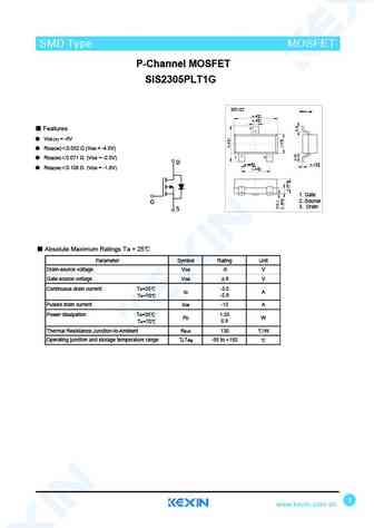
SMD Type MOSFET SMD Type P-Channel MOSFET SIS2305PLT1G SOT-23 Unit mm 2.9+0.1 -0.1 +0.1 0.4-0.1 3 Features VDS (V) = -8V RDS(ON) 0.052 (VGS = -4.5V) 1 2 RDS(ON) 0.071 (VGS = -2.5V) D +0.1 +0.05 0.95 -0.1 0.1 -0.01 RDS(ON) 0.108 (VGS = -1.8V) +0.1 1.9 -0.1 1. Gate 2. Source G 3. Drain S Absolute Maximum Ratings Ta = 25 Para
am2305.pdf
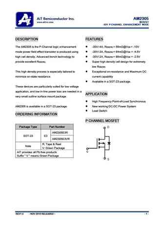
AiT Semiconductor Inc. AM2305 www.ait-ic.com MOSFET -30V P-CHANNEL ENHANCEMENT MODE DESCRIPTION FEATURES The AM2305 is the P-Channel logic enhancement -30V/-4A, R = 55m @V = -10V DS(ON) GS mode power field effect transistor is produced using -30V/-3A, R = 64m @V = -4.5V DS(ON) GS high cell density. Advanced trench technology to -30V/-2A, R = 85m @V = -2.5V DS(ON)
blm2305.pdf
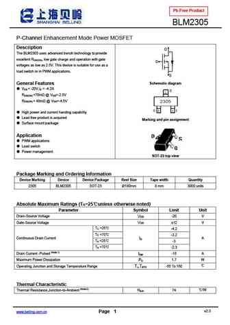
Pb Free Product BLM2305 P-Channel Enhancement Mode Power MOSFET Description D The BLM2305 uses advanced trench technology to provide excellent R , low gate charge and operation with gate DS(ON) G voltages as low as 2.5V. This device is suitable for use as a load switch or in PWM applications. S Schematic diagram General Features V = -20V,I = -4.2A DS D RDS(ON)
chm2305gp.pdf
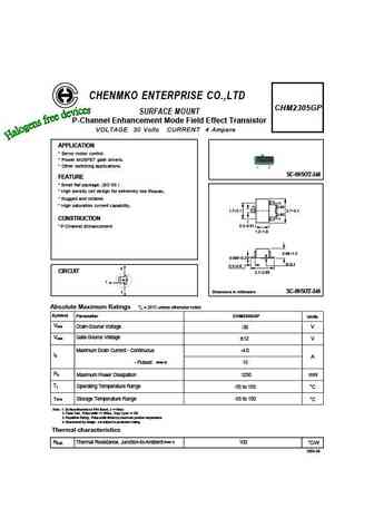
CHENMKO ENTERPRISE CO.,LTD CHM2305GP SURFACE MOUNT P-Channel Enhancement Mode Field Effect Transistor VOLTAGE 30 Volts CURRENT 4 Ampere APPLICATION * Servo motor control. * Power MOSFET gate drivers. * Other switching applications. SC-59/SOT-346 FEATURE * Small flat package. (SC-59 ) * High density cell design for extremely low RDS(ON). * Rugged and reliable. (2) * High satur
bl2305.pdf
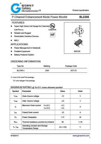
Product specification P-Channel Enhancement Mode Power Mosfet BL2305 FEATURES Super High Dense Cell Design for Extremely Pb Low R Lead-free DS(ON) Reliable and Rugged Electrostatic Sensitive Devices. MSL1 APPLICATIONS Power Management in Notebook. Portable Equipment. SOT-23 Battery Powered System. ORDERING INFORMATION Type No. Marking P
kia2305.pdf
-3.5A -20V 2305 P-CHANNELMOSFET KIA KIA KIA SEMICONDUCTORS SEMICONDUCTORS SEMICONDUCTORS 1. Features V =-20V,R =0.055 @V =-4.5V,I =-3.5A DS DS(on) GS D V =-20V,R =0.075 @V =-2.5V,I =-3.0A DS DS(on) GS D V =-20V,R =0.095 @V =-1.8V,I =-1.8A DS DS(on) GS D 2.Symbol Pin Function 1 Gate 2 Source 3 Drain 3. Absolute maximumratings Parameter Symbol Rating Units Drain-sou
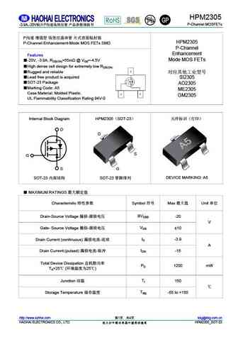
me2305 me2305-g.pdf
ME2305/ME2305-G P-Channel 20V (D-S) MOSFET GENERAL DESCRIPTION FEATURES The ME2305 is the P-Channel logic enhancement mode power RDS(ON) 62m @VGS=-10V field effect transistors are produced using high cell density, DMOS RDS(ON) 72m @VGS=-4.5V trench technology. This high density process is especially tailored RDS(ON) 91m @VGS=-2.5V to minimize on-state resista
me2305a me2305a-g.pdf
ME2305A/ME2305A-G P-Channel 20V (D-S) MOSFET GENERAL DESCRIPTION FEATURES The ME2305A is the P-Channel logic enhancement mode power RDS(ON) 67m @VGS=-10V field effect transistors are produced using high cell density, DMOS RDS(ON) 77m @VGS=-4.5V trench technology. This high density process is especially tailored RDS(ON) 96m @VGS=-2.5V to minimize on-state resistan
nce2305a.pdf
Pb Free Product http //www.ncepower.com NCE2305A NCE P-Channel Enhancement Mode Power MOSFET D Description The NCE2305A uses advanced trench technology to provide G excellent RDS(ON), low gate charge and operation with gate voltages as low as 2.5V. This device is suitable for use as a load switch or in PWM applications. S Schematic diagram General Features VDS = -12V,
nce2305.pdf
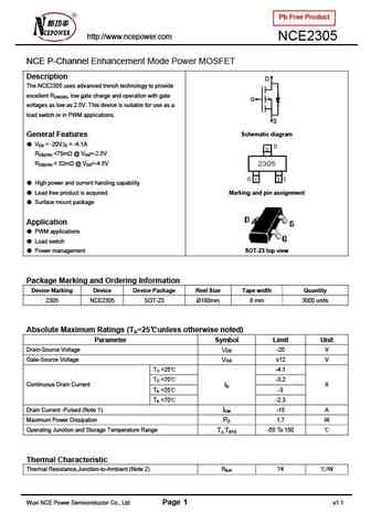
Pb Free Product http //www.ncepower.com NCE2305 NCE P-Channel Enhancement Mode Power MOSFET Description D The NCE2305 uses advanced trench technology to provide excellent RDS(ON), low gate charge and operation with gate G voltages as low as 2.5V. This device is suitable for use as a load switch or in PWM applications. S Schematic diagram General Features VDS = -20V,ID
stp2305.pdf
STP2305 -30V P-Channel Enhancement Mode MOSFET DESCRIPTION FEATURE The STP2305 is the P-Channel logic enhancement -30V/-4.3A, RDS(ON) =55m (typ.)@VGS =-10V mode power field effect transistor is produced using -30V/-3.5A, RDS(ON) =65m (typ.)@VGS =-4.5V high cell density. advanced trench technology to -30V/-2.5A, RDS(ON) =87m (typ.)@VGS =-2.5V provide exce
ssm2305gn.pdf
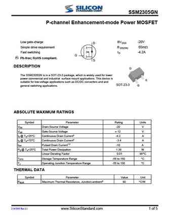
SSM2305GN P-channel Enhancement-mode Power MOSFET Low gate-charge BVDSS -20V D Simple drive requirement R 65m DS(ON) Fast switching ID -4.2A G Pb-free; RoHS compliant. S DESCRIPTION D The SSM2305GN is in a SOT-23-3 package, which is widely used for lower power commercial and industrial surface mount applications. This device is S suitable for low-voltage applications such as
ssm2305agn.pdf

SSM2305AGN P-channel Enhancement-mode Power MOSFET Low gate-charge BVDSS -30V D Simple drive requirement R 80m DS(ON) Fast switching ID -3.2A G Pb-free; RoHS compliant. S DESCRIPTION D The SSM2305AGN is in a SOT-23-3 package, which is widely used for lower power commercial and industrial surface mount applications. This device is S suitable for low-voltage applications such a
sl2305.pdf
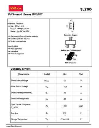
SL2305 P-Channel Power MOSFET D General Features G VDS = -20V,ID = -4.1A RDS(ON)
st2305.pdf
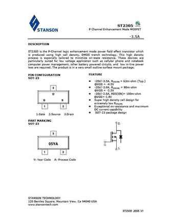
ST2305 P Channel Enhancement Mode MOSFET -3.5A DESCRIPTION ST2305 is the P-Channel logic enhancement mode power field effect transistor which is produced using high cell density, DMOS trench technology. This high density process is especially tailored to minimize on-state resistance. These devices are particularly suited for low voltage application such as cellular phone and not
st2305a.pdf

ST2305A P Channel Enhancement Mode MOSFET -3.5A DESCRIPTION ST2305A is the P-Channel logic enhancement mode power field effect transistor which is produced using high cell density, DMOS trench technology. This high density process is especially tailored to minimize on-state resistance. These devices are particularly suited for low voltage application such as cellular phone and no
si2305a.pdf
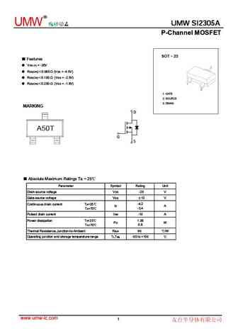
R UMW SI2305A UMW SI2305A UMW P-Channel MOSFET SOT 23 Features VDS (V) = -20V RDS(ON) 0.065 (VGS = -4.5V) RDS(ON) 0.100 (VGS = -2.5V) RDS(ON) 0.250 (VGS = -1.8V) 1. GATE 2. SOURCE 3. DRAIN MARKING D A50T G S Absolute Maximum Ratings Ta = 25 Parameter Symbol Rating Unit Drain-source voltage VDS -20 V Gate-source voltage VG
atm2305psa.pdf
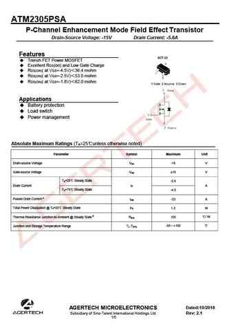
ATM2305PSA P-Channel Enhancement Mode Field Effect Transistor Drain-Source Voltage -15V Drain Current -5.6A Features Trench FET Power MOSFET Excellent RDS(on) and Low Gate Charge RDS(ON)( at VGS=-4.5V) 36.4 mohm RDS(ON)( at VGS=-2.5V) 53.0 mohm RDS(ON)( at VGS=-1.8V) 62.0 mohm Applications Battery protection Load switch Power manag
as2305.pdf
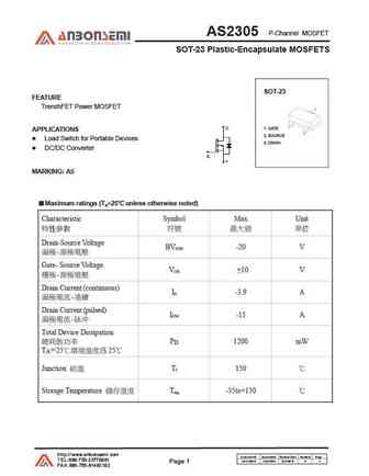
P-Channel MOSFET AS2305 SOT-23 Plastic-Encapsulate MOSFETS SOT-23 FEATURE TrenchFET Power MOSFET 1. GATE APPLICATIONS 2. SOURCE Load Switch for Portable Devices 3. DRAIN DC/DC Converter MARKING A5 Maximum ratings (Ta=25 unless otherwise noted) Characteristic Symbol Max Unit Drain-Source Voltage BV -20 V DSS -
si2305.pdf
SI2305 MOSFET ROHS P-Channel MOSFET SOT-23 - Features Advanced trench process technology High Density Cell Design For Ultra Low On-Resistance Maximum Ratings & Thermal Characteristics (Ratings at 25 ambient temperature unless otherwise specified.) Parameter Symbol Limit Unit Drain-Source Voltage VDS -20 V Gate-Source Voltage 12 VGS ID Continuous Drain
ctz2305a.pdf
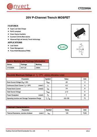
nvert CTZ2305A Suzhou Convert Semiconductor Co ., Ltd. 20V P-Channel Trench MOSFET FEATURES Super Low Gate Charge RoHS compliant Green Device Available Excellent CdV/dt effect decline Advanced high cell density Trench technology APPLICATIONS Load Switch Power Management Pulse Width Modulation(PWM) Device Marking and Package Information Device Packa
en2305.pdf
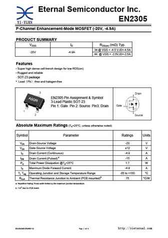
Eternal Semiconductor Inc. EN2305 P-Channel Enhancement-Mode MOSFET (-20V, -4.9A) PRODUCT SUMMARY VDSS ID RDS(on) (m ) Typ. 34 @ VGS = -4.5 V,ID=-4.5A -20V -4.9A 44 @ VGS = -2.5V,ID=-2.5A Features Super high dense cell trench design for low RDS(on) Rugged and reliable SOT-23 package Lead Pb -free and halogen-free EN2305 Pin Assignment & Symbol 3-Lead Plastic S
si2305.pdf
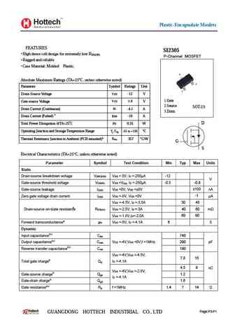
Plastic-Encapsulate Mosfets FEATURES SI2305 High dense cell design for extremely low RDS(ON) P-Channel MOSFET Rugged and reliable Case Material Molded Plastic. Absolute Maximum Ratings (TA=25oC, unless otherwise noted) Parameter Symbol Ratings Unit Drain-Source Voltage VDS -12 V 1.Gate Gate-source Voltage VGS 8 V 2.Source SOT-23 Drain Current (Continuous) ID -4.1 A 3.Drain a
hss2305a.pdf
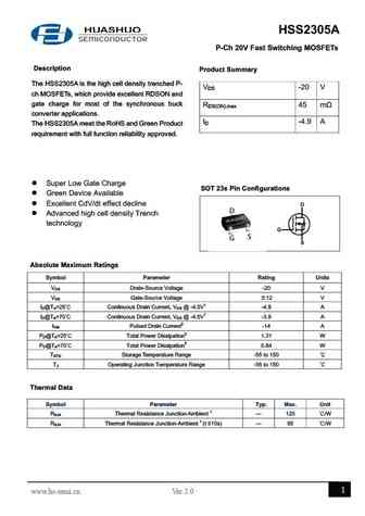
HSS2305A P-Ch 20V Fast Switching MOSFETs Description Product Summary The HSS2305A is the high cell density trenched P- VDS -20 V ch MOSFETs, which provide excellent RDSON and gate charge for most of the synchronous buck RDS(ON),max 45 m converter applications. ID -4.9 A The HSS2305A meet the RoHS and Green Product requirement with full function reliability approved. l
hx2305.pdf
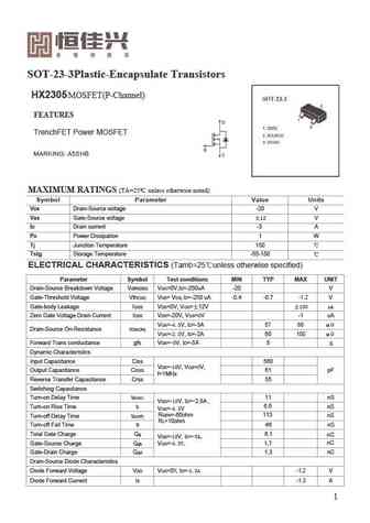
SOT-23-3Plastic-Encapsulate Transistors HX2305MOSFET(P-Channel) FEATURES TrenchFET Power MOSFET MARKING A5SHB MAXIMUM RATINGS (TA=25 unless otherwise noted) Symbol Parameter Value Units VDS Drain-Source voltage -20 V VGS Gate-Source voltage 12 V -3 A ID Drain current PD Power Dissipation 1 W Tj Junction Temperature 150 Tstg Storage Temperature -55-150 ELECTRICAL CHAR
hd2305.pdf
HD2305 SOT-23 Plastic-Encapsulate MOSFET P -Channel MOSFET roduct Summary P ID V(BR)DSS RDS(on)MAX SOT- 23 45m @-4.5V D -12V 60m @-2.5V -4.1A 90m @-1.8V S Features TrenchFET Power MOSFET G Applications Load Switch for Portable Devices DC/DC Converter Marking S5 Symbol Value Parameter Unit Drain-Source Voltage VDS -12 V Gate-
jmtl2305a.pdf
JMTL2305A Description JMT P-channel Enhancement Mode Power MOSFET Features Application V = -20V, I = -4.1A PWM Applications DS D R
jmtv2305a.pdf
JMTV2305A Description JMT P-channel Enhancement Mode Power MOSFET Features Application V = -20V, I = -7A PWM Applications DS D R
jmtl2305b1.pdf
JMTL2305B Description JMT P-channel Enhancement Mode Power MOSFET Features Application V =-12V, I =-4.1A PWM Applications DS D R
si2305.pdf
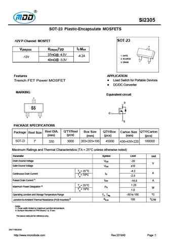
SI2305 SOT-23 Plastic-Encapsulate MOSFETS SOT-23 -12V P-Channel MOSFET 3 ID Max V(BR)DSS RDS(on)Typ 37m @ -4.5V 1. GATE -4.2A -12V 2. SOURCE 40m @ -3.3V 1 3. DRAIN 2 APPLICATION Features Load Switch for Portable Devices Trench FET Power MOSFET DC/DC Converter MARKING Equivalent circuit D S5 G S PACKAGE SPECIFICATIONS Reel DIA. Q'TY/Reel
pjm2305psa.pdf
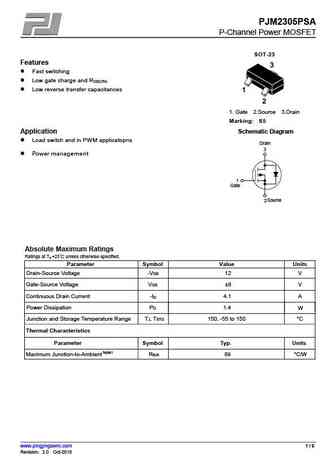
PJM2305PSA P-Channel Power MOSFET SOT-23 Features Fast switching Low gate charge and R DS(ON) Low reverse transfer capacitances 1. Gate 2.Source 3.Drain Marking S5 Application Schematic Diagram Load switch and in PWM applicatopns Drain 3 Power management 1 Gate Source 2 Absolute Maximum Ratings Ratings at TA =25 unless otherwise specified. Paramete
wtm2305.pdf
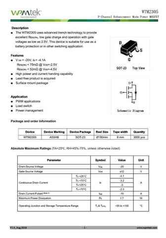
WTM2305 P-Channel Enhancement Mode Power MOSFET Description The WTM2305 uses advanced trench technology to provide excellent R , low gate charge and operation with gate DS(ON) voltages as low as 2.5V. This device is suitable for use as a battery protection or in other switching application. Features V DS = -20V, lD = -4.1A R
si2305.pdf
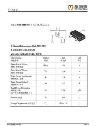
SI2305 SOT-23 (SOT-23 Field Effect Transistors) P-Channel Enhancement-Mode MOS FETs P MOS MAXIMUM RATINGS Characteristic Symbol Rat Unit Drain-Source Voltage BV -20 V DSS - Gate- Source Voltage V +10 V GS - Drain Current (continuous) I -3.9 A D
si2305.pdf
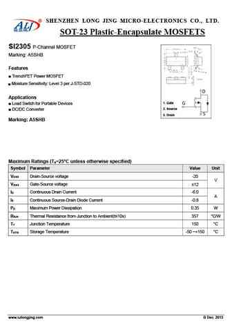
SHENZHEN LONG JING MICRO-ELECTRONICS CO., LTD. SOT-23 Plastic-Encapsulate MOSFETS SI2305 P-Channel MOSFET Marking A5SHB Features TrenchFET Power MOSFET Moisture Sensitivity Level 3 per J-STD-020 Applications 1. Gate Load Switch for Portable Devices 2. Source DC/DC Converter 3. Drain Marking A5SHB Maximum Ratings (T =25 C unless otherwise specified) a S
si2305.pdf
SI2305 AO3401 SI2305 SOT-23 Plastic-Encapsulate MOSFETS P-Channel 12-V( D-S) MOSFET FEATURE TrenchFET Power MOSFET APPLICATIONS z Load Switch for Portable Devices z DC/DC Converter MARKING Equivalent Circuit A09T A19T 2305 1.GATE 1.GATE 2.SOURCE 2.SOURCE 3.DRAIN 3.DRAIN Maximum ratings (Ta=25 unless otherwise noted) Parameter Symbol Value Unit Drain-Source Voltag
wst2305a.pdf
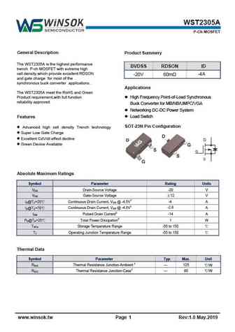
WST2305A P-Ch MOSFET General Description Product Summery The WST2305A is the highest performance BVDSS RDSON ID trench P-ch MOSFET with extreme high cell density,which provide excellent RDSON -4A -20V 60m and gate charge for most of the synchronous buck converter applications . Applications The WST2305A meet the RoHS and Green Product requirement,with full function Hi
wst2305.pdf
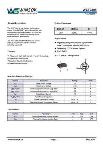
WST2305 P-Ch MOSFET General Description Product Summery The WST2305 is the highest performance BVDSS RDSON ID trench P-ch MOSFET with extreme high cell density,which provide excellent RDSON and -4.4A -20V 50m gate charge for most of the synchronous buck converter applications . Applications The WST2305 meet the RoHS and Green Product requirement,with full function H
se2305.pdf
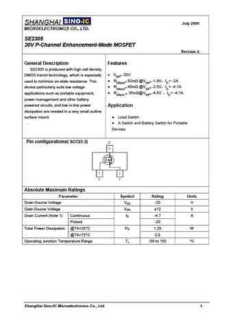
SHANGHAI July 2005 MICROELECTRONICS CO., LTD. SE2305 20V P-Channel Enhancement-Mode MOSFET Revision A General Description Features SE2305 is produced with high cell density VDS= -20V DMOS trench technology, which is especially RDS(on)= 52m @VGS= -1.8V ID = -2A used to minimize on-state resistance. This RDS(on)= 40m @VGS= -2.5V ID = -4.1A device part
se2305a.pdf
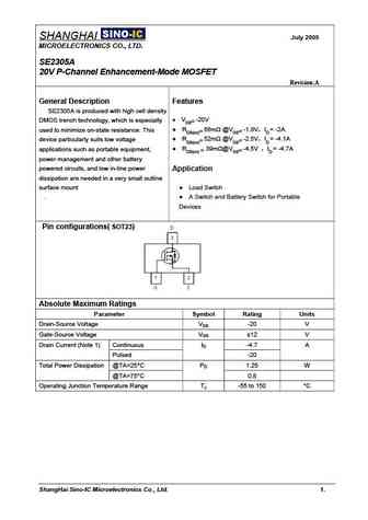
SHANGHAI July 2005 MICROELECTRONICS CO., LTD. SE2305A 20V P-Channel Enhancement-Mode MOSFET Revision A General Description Features SE2305A is produced with high cell density VDS= -20V DMOS trench technology, which is especially RDS(on)= 68m @VGS= -1.8V ID = -2A used to minimize on-state resistance. This RDS(on)= 52m @VGS= -2.5V ID = -4.1A device pa
sm2305.pdf
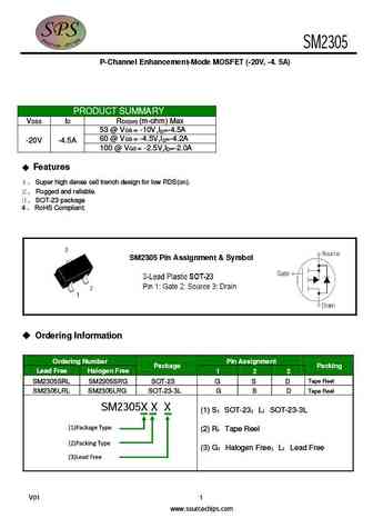
SM2305 P-Channel Enhancement-Mode MOSFET (-20V, -4. 5A) PRODUCT SUMMARY VDSS ID RDS(on) (m-ohm) Max 53 @ VGS = -10V,ID=-4.5A 60 @ VGS = -4.5V,ID=-4.2A -20V -4.5A 100 @ VGS = -2.5V,ID=-2.0A Features 1 Super high dense cell trench design for low RDS(on). 2 Rugged and reliable. 3 SOT-23 package 4 RoHS Compliant. SM2305 Pin Assignment & Symbol
apm2305ac.pdf
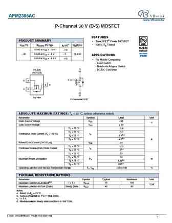
APM2305AC www.VBsemi.tw P-Channel 30 V (D-S) MOSFET FEATURES PRODUCT SUMMARY TrenchFET Power MOSFET 100 % Rg Tested VDS (V) RDS(on) ( ) Typ. ID (A)a Qg (Typ.) 0.046 at VGS = - 10 V - 5.6 0.049 at VGS = - 6 V - 5 11.4 nC - 30 APPLICATIONS 0.054 at VGS = - 4.5 V -4.5 For Mobile Computing - Load Switch - Notebook Adaptor Switch S TO-236 - DC/DC Converter (SOT-2
vbqa2305.pdf
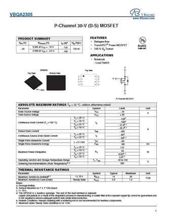
VBQA2305 www.VBsemi.com P-Channel 30-V (D-S) MOSFET FEATURES PRODUCT SUMMARY Halogen-free VDS (V) RDS(on) ( ) ID (A)a Qg (Typ.) TrenchFET Power MOSFET RoHS 0.004 at VGS = - 10 V - 120 COMPLIANT - 30 130 nC 100 % Rg Tested 0.006 at VGS = - 4.5 V - 100 APPLICATIONS Notebook - Load Switch S DFN5X6 Top View Top View Bottom View 1 8 G 2 7 3 6 4
si2305cds-t1-ge3.pdf
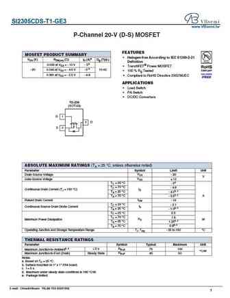
SI2305CDS-T1-GE3 www.VBsemi.tw P-Channel 20-V (D-S) MOSFET FEATURES MOSFET PRODUCT SUMMARY Halogen-free According to IEC 61249-2-21 VDS (V) RDS(on) ( )ID (A)a Qg (Typ.) Definition 0.035 at VGS = - 10 V - 5e TrenchFET Power MOSFET e - 20 0.043 at VGS = - 4.5 V - 5 10 nC 100 % Rg Tested 0.061 at VGS = - 2.5 V - 4.8 Compliant to RoHS Directive 2002/95/EC APPLICA
ap2305agn.pdf
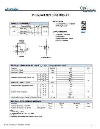
AP2305AGN www.VBsemi.tw P-Channel 30 V (D-S) MOSFET FEATURES PRODUCT SUMMARY TrenchFET Power MOSFET 100 % Rg Tested VDS (V) RDS(on) ( ) Typ. ID (A)a Qg (Typ.) 0.046 at VGS = - 10 V - 5.6 0.049 at VGS = - 6 V - 5 11.4 nC - 30 APPLICATIONS 0.054 at VGS = - 4.5 V -4.5 For Mobile Computing - Load Switch - Notebook Adaptor Switch S TO-236 - DC/DC Converter (SOT-2
cmn2305m.pdf

CMN2305M www.VBsemi.tw P-Channel 20-V (D-S) MOSFET FEATURES MOSFET PRODUCT SUMMARY Halogen-free According to IEC 61249-2-21 VDS (V) RDS(on) ( )ID (A)a Qg (Typ.) Definition 0.035 at VGS = - 10 V - 5e TrenchFET Power MOSFET e - 20 0.043 at VGS = - 4.5 V - 5 10 nC 100 % Rg Tested 0.061 at VGS = - 2.5 V - 4.8 Compliant to RoHS Directive 2002/95/EC APPLICATION
sts2305a.pdf

STS2305A www.VBsemi.tw P-Channel 20-V (D-S) MOSFET FEATURES MOSFET PRODUCT SUMMARY Halogen-free According to IEC 61249-2-21 VDS (V) RDS(on) ( )ID (A)a Qg (Typ.) Definition 0.035 at VGS = - 10 V - 5e TrenchFET Power MOSFET e - 20 0.043 at VGS = - 4.5 V - 5 10 nC 100 % Rg Tested 0.061 at VGS = - 2.5 V - 4.8 Compliant to RoHS Directive 2002/95/EC APPLICATION
am2305pe.pdf
AM2305PE www.VBsemi.tw P-Channel 30 V (D-S) MOSFET FEATURES PRODUCT SUMMARY TrenchFET Power MOSFET 100 % Rg Tested VDS (V) RDS(on) ( ) Typ. ID (A)a Qg (Typ.) 0.046 at VGS = - 10 V - 5.6 0.049 at VGS = - 6 V - 5 11.4 nC - 30 APPLICATIONS 0.054 at VGS = - 4.5 V -4.5 For Mobile Computing - Load Switch - Notebook Adaptor Switch S TO-236 - DC/DC Converter (SOT-23
vbe2305.pdf
VBE2305 www.VBsemi.com P-Channel 30 V (D-S) MOSFET FEATURES PRODUCT SUMMARY Compliant to RoHS Directive 2002/95/EC VDS (V) RDS(on) ( )ID (A)a Available 0.005 at VGS = - 10 V -100 RoHS* - 30 COMPLIANT 0.007 at VGS = - 4.5 V -90 S TO-252 G D G S D Top View P-Channel MOSFET ABSOLUTE MAXIMUM RATINGS (TC = 25 C, unless otherwise noted) Parameter Symbol Limit Unit Gate
vba2305.pdf
VBA2305 www.VBsemi.com P-Channel 30 V (D-S) MOSFET FEATURES PRODUCT SUMMARY TrenchFET Gen IV p-channel power MOSFET VDS (V) -30 RDS(on) max. ( ) at VGS = 10 V 0.0050 Enables higher power density RDS(on) max. ( ) at VGS = 4.5 V 0.0080 100 % Rg and UIS tested Qg typ. (nC) 27 ID (A) 18 Configuration Single APPLICATIONS SO-8 Single S D Battery management in m
si2305ads-t1-ge3.pdf

SI2305ADS-T1-GE3 www.VBsemi.tw P-Channel 20-V (D-S) MOSFET FEATURES MOSFET PRODUCT SUMMARY Halogen-free According to IEC 61249-2-21 VDS (V) RDS(on) ( )ID (A)a Qg (Typ.) Definition 0.035 at VGS = - 10 V - 5e TrenchFET Power MOSFET e - 20 0.043 at VGS = - 4.5 V - 5 10 nC 100 % Rg Tested 0.061 at VGS = - 2.5 V - 4.8 Compliant to RoHS Directive 2002/95/EC APPLICA
nce2305a.pdf
NCE2305A www.VBsemi.tw P-Channel 30 V (D-S) MOSFET FEATURES PRODUCT SUMMARY TrenchFET Power MOSFET 100 % Rg Tested VDS (V) RDS(on) ( ) Typ. ID (A)a Qg (Typ.) 0.046 at VGS = - 10 V - 5.6 0.049 at VGS = - 6 V - 5 11.4 nC - 30 APPLICATIONS 0.054 at VGS = - 4.5 V -4.5 For Mobile Computing - Load Switch - Notebook Adaptor Switch S TO-236 - DC/DC Converter (SOT-23
si2305ds-t1-ge3.pdf
SI2305DS-T1-GE3 www.VBsemi.tw P-Channel 20-V (D-S) MOSFET FEATURES MOSFET PRODUCT SUMMARY Halogen-free According to IEC 61249-2-21 VDS (V) RDS(on) ( )ID (A)a Qg (Typ.) Definition 0.035 at VGS = - 10 V - 5e TrenchFET Power MOSFET e - 20 0.043 at VGS = - 4.5 V - 5 10 nC 100 % Rg Tested 0.061 at VGS = - 2.5 V - 4.8 Compliant to RoHS Directive 2002/95/EC APPLICAT
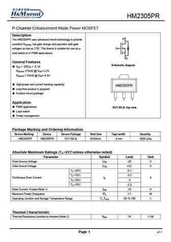
hm2305pr.pdf
HM2305PR www.VBsemi.tw P-Channel 30-V (D-S) MOSFET FEATURES PRODUCT SUMMARY Halogen-free According to IEC 61249-2-21 VDS (V) RDS(on) ( ) ID (A)d Qg (Typ.) Definition 0.050 at VGS = - 10 V - 7.6 TrenchFET Power MOSFET - 30 13 nC 100 % Rg Tested 0.056 at VGS = - 4.5 V - 6.0 APPLICATIONS Load Switch Battery Switch D S G G D S D P-Channel MOSFET ABS
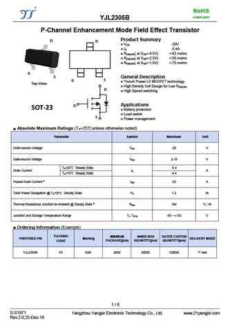
yjl2305a.pdf
RoHS COMPLIANT YJL2305A P-Channel Enhancement Mode Field Effect Transistor Product Summary V -15V DS I -5.6A D R ( at V =-4.5V) 36.4 mohm DS(ON) GS R ( at V =-2.5V) 53.0 mohm DS(ON) GS R ( at V =-1.8V) 70.0 mohm DS(ON) GS General Description Trench Power LV MOSFET technology High Density Cell Design for Low R DS(ON) High
yjl2305b.pdf
RoHS COMPLIANT YJL2305B P-Channel Enhancement Mode Field Effect Transistor Product Summary V -20V DS I -5.4A D R ( at V =-4.5V) 42 mohm DS(ON) GS R ( at V =-2.5V) 55 mohm DS(ON) GS R ( at V =-1.8V) 75 mohm DS(ON) GS General Description Trench Power LV MOSFET technology High Density Cell Design for Low R DS(ON) High Speed
ttx2305a.pdf
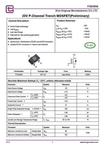
TTX2305A Wuxi Unigroup Microelectronics CO.,LTD. 20V P-Channel Trench MOSFET(Preliminary) Product Summary General Description VDS -20V Trench Power technology ID (at VGS =-10V) -4.5A Low RDS(ON) RDS(ON) (at VGS =-10V)
hm2305b.pdf
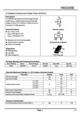
HM2305B P-Channel Enhancement Mode Power MOSFET Description D The HM2305B uses advanced trench technology to provide excellent RDS(ON), low gate charge and operation with gate G voltages as low as 2.5V. This device is suitable for use as a load switch or in PWM applications. S Schematic diagram General Features VDS = -12V,ID = -4.1A RDS(ON)
hm2305d.pdf
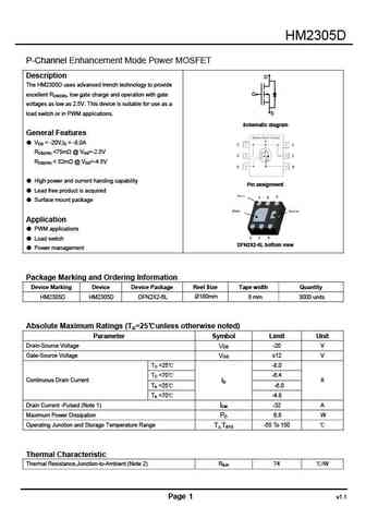
HM2305D P-Channel Enhancement Mode Power MOSFET Description D The HM2305D uses advanced trench technology to provide excellent RDS(ON), low gate charge and operation with gate G voltages as low as 2.5V. This device is suitable for use as a S load switch or in PWM applications. Schematic diagram General Features VDS = -20V,ID = -8.0A RDS(ON)
hm2305pr.pdf
HM2305PR P-Channel Enhancement Mode Power MOSFET Description D The HM2305PR uses advanced trench technology to provide excellent RDS(ON), low gate charge and operation with gate voltages as low as 2.5V. This device is suitable for use as a G load switch or in PWM applications. S General Features Schematic diagram VDS = -20V,ID = - .1A RDS(ON)
hm2305.pdf
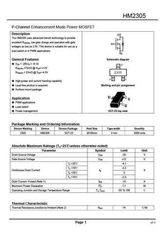
P-Channel Enhancement Mode Power MOSFET Description D The uses advanced trench technology to provide excellent RDS(ON), low gate charge and operation with gate G voltages as low as 2.5V. This device is suitable for use as a load switch or in PWM applications. S Schematic diagram General Features VDS = -20V,ID = -4.1A RDS(ON)
hpm2305.pdf
HPM2305 P-Channel MOSFETs -3.9A,-20V P P HPM2305 P-Channel Enhancement-Mode MOS FETs SMD P-Channel Enhancement Features Mode MOS FETs -20V, -3.9A, RDS(ON)=55m @ VGS=-4.5V High dense cell design for extremely low RDS(ON) Rugged and reliable
2sc2305.pdf
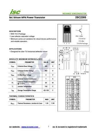
INCHANGE Semiconductor isc Silicon NPN Power Transistor 2SC2305 DESCRIPTION With TO-3 Package Low collector saturation voltage Minimum Lot-to-Lot variations for robust device performance and reliable operation. APPLICATIONS Designed for color TV horizontal deflection driver ABSOLUTE MAXIMUM RATINGS(T =25 ) a SYMBOL PARAMETER VALUE UNIT V Collector-Base Voltage 400 V CBO
ap2305bi.pdf
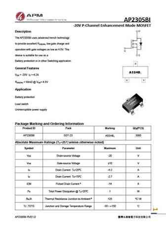
AP2305BI -20V P-Channel Enhancement Mode MOSFET Description The AP2305BI uses advanced trench technology to provide excellent R , low gate charge and DS(ON) operation with gate voltages as low as 4.5V. This device is suitable for use as a Battery protection or in other Switching application. General Features V = -20V I =-4.2A DS D R
ap2305mi.pdf
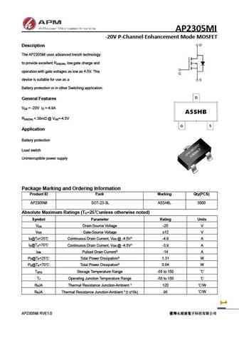
AP2305MI -20V P-Channel Enhancement Mode MOSFET Description The AP2305MI uses advanced trench technology to provide excellent R , low gate charge and DS(ON) operation with gate voltages as low as 4.5V. This device is suitable for use as a Battery protection or in other Switching application. General Features V = -20V I =-4.9A DS D R
ap2305ai.pdf
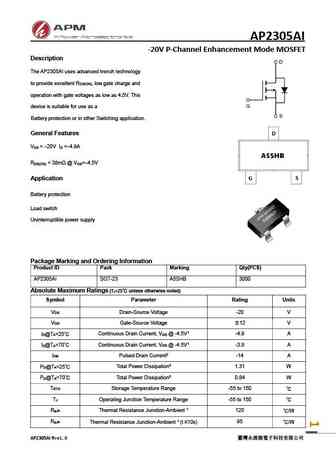
AP2305AI -20V P-Channel Enhancement Mode MOSFET Description The AP2305AI uses advanced trench technology to provide excellent R , low gate charge and DS(ON) operation with gate voltages as low as 4.5V. This device is suitable for use as a Battery protection or in other Switching application. General Features V = -20V I =-4.9A DS D R
Другие MOSFET... 2N6800LCC4 , 2N6800U , 2N6802U , 2N6845LCC4 , 2N6845U , 2N6847U , 2303 , 2304 , STP80NF70 , 4414 , 4614 , 4800 , 8958 , 9926 , 045Y , 06N03 , 10N60A .
History: AOC3860C | D2N60
🌐 : EN ES РУ

Список транзисторов
Обновления
MOSFET: AUB034N10 | AUB033N08BG | AUB026N085 | AUA062N08BG | AUA060N08AG | AUA056N08BGL | AUA039N10 | ASW80R290E | ASW65R120EFD | ASW65R110E | ASW65R095EFD | ASW65R046EFD | ASW65R041EFDA | ASW65R041E | ASW60R150E | ASW60R090EFDA
Popular searches
bc547 datasheet | k3797 mosfet | bs170 datasheet | tip41c | irfp460 | irfz44n mosfet | lm317t datasheet | irf540