50N15. Аналоги и основные параметры
Наименование производителя: 50N15
Тип транзистора: MOSFET
Полярность: N
Предельные значения
Pd ⓘ
- Максимальная рассеиваемая мощность: 220 W
|Vds|ⓘ - Максимально допустимое напряжение сток-исток: 150 V
|Vgs|ⓘ - Максимально допустимое напряжение затвор-исток: 20 V
|Id| ⓘ - Максимально допустимый постоянный ток стока: 50 A
Tj ⓘ - Максимальная температура канала: 150 °C
Электрические характеристики
RDSonⓘ - Сопротивление сток-исток открытого транзистора: 0.023 Ohm
Тип корпуса: TO-220C
Аналог (замена) для 50N15
- подборⓘ MOSFET транзистора по параметрам
50N15 даташит
..1. Size:215K inchange semiconductor
50n15.pdf 
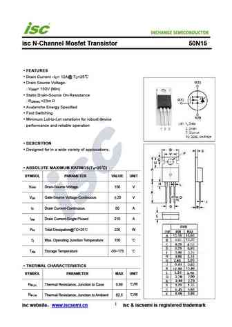
INCHANGE Semiconductor isc N-Channel Mosfet Transistor 50N15 FEATURES Drain Current I = 12A@ T =25 D C Drain Source Voltage- V = 150V (Min) DSS Static Drain-Source On-Resistance R
0.1. Size:468K 1
mte050n15brv8.pdf 
Spec. No. C033V8 Issued Date 2017.10.05 CYStech Electronics Corp. Revised Date Page No. 1/9 N-Channel Enhancement Mode Power MOSFET MTE050N15BRV8 BVDSS 150V ID @ TC=25 C, VGS=10V 12.4A ID @ TA=25 C, VGS=10V 4.3A 49.1m VGS=10V, ID=3.4A Features RDSON(TYP) 58.5m VGS=6V, ID=3.3A Single Drive Requirement Low On-resistance Fast Switchi
0.2. Size:858K 1
mte050n15brh8.pdf 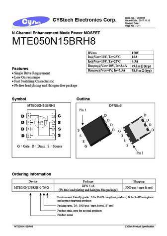
Spec. No. C033H8 Issued Date 2017.11.15 CYStech Electronics Corp. Revised Date Page No. 1/11 N-Channel Enhancement Mode Power MOSFET MTE050N15BRH8 BVDSS 150V ID@VGS=10V, TC=25 C 16A ID@VGS=10V, TA=25 C 4.3A RDS(ON)@VGS=10V, ID=3.4A 49.1m (typ) Features RDS(ON)@VGS=6V, ID=3.3A 58.5 m (typ) Single Drive Requirement Low On-resistance Fast Switchi
0.3. Size:252K ixys
ixtk150n15p ixtq150n15p.pdf 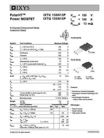
IXTK 150N15P PolarHTTM VDSS = 150 V IXTQ 150N15P Power MOSFET ID25 = 150 A RDS(on) 13 m N-Channel Enhancement Mode Avalanche Rated TO-264 (IXTK) Symbol Test Conditions Maximum Ratings VDSS TJ = 25 C to 175 C 150 V VDGR TJ = 25 C to 175 C; RGS = 1 M 150 V G D (TAB) VGS Continuous 20 V D S VGSM Transient 30 V ID25 TC = 25
0.4. Size:252K ixys
ixfh150n15p ixfk150n15p.pdf 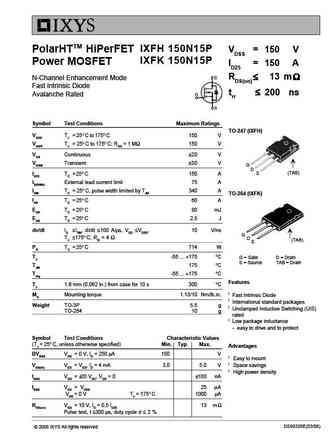
IXFH 150N15P PolarHTTM HiPerFET VDSS = 150 V IXFK 150N15P Power MOSFET ID25 = 150 A RDS(on) 13 m N-Channel Enhancement Mode Fast Intrinsic Diode trr 200 ns Avalanche Rated Symbol Test Conditions Maximum Ratings TO-247 (IXFH) VDSS TJ = 25 C to 175 C 150 V VDGR TJ = 25 C to 175 C; RGS = 1 M 150 V VGS Contin
0.5. Size:47K ixys
ixfk150n15 ixfx150n15.pdf 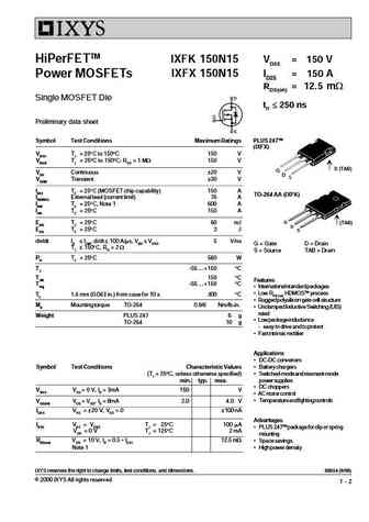
HiPerFETTM IXFK 150N15 VDSS = 150 V IXFX 150N15 ID25 = 150 A Power MOSFETs RDS(on) = 12.5 mW Single MOSFET Die trr 250 ns Preliminary data sheet Symbol Test Conditions Maximum Ratings PLUS 247TM (IXFX) VDSS TJ = 25 C to 150 C 150 V VDGR TJ = 25 C to 150 C; RGS = 1 MW 150 V D (TAB) G VGS Continuous 20 V D VGSM Transient 30 V ID25 TC = 25 C (MOSFET chip capability) 150
0.6. Size:70K ixys
ixfn150n15.pdf 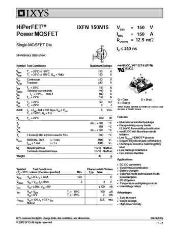
HiPerFETTM IXFN 150N15 VDSS = 150 V ID25 = 150 A Power MOSFET RDS(on) = 12.5 mW Single MOSFET Die trr 250 ns Preliminary data sheet miniBLOC, SOT-227 B (IXFN) Symbol Test Conditions Maximum Ratings E153432 VDSS TJ = 25 C to 150 C 150 V S VDGR TJ = 25 C to 150 C, RGS = 1MW 150 V G VGS Continuous 20 V VGSM Transient 30 V ID25 TC = 25 C 150 A S IL(RMS) Terminal (curre
0.7. Size:382K cystek
mte50n15j3.pdf 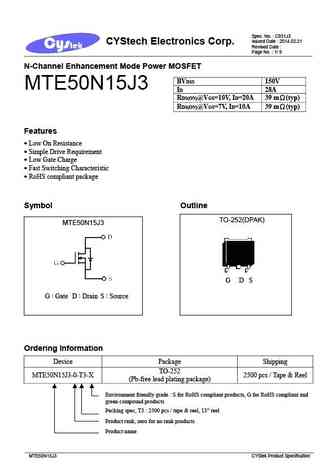
Spec. No. C931J3 Issued Date 2014.02.21 CYStech Electronics Corp. Revised Date Page No. 1/ 9 N-Channel Enhancement Mode Power MOSFET BVDSS 150V MTE50N15J3 ID 28A RDS(ON)@VGS=10V, ID=20A 39 m (typ) RDS(ON)@VGS=7V, ID=10A 39 m (typ) Features Low On Resistance Simple Drive Requirement Low Gate Charge Fast Switching Characteristic RoHS com
0.8. Size:299K cystek
mte50n15fp.pdf 
Spec. No. C931FP Issued Date 2013.12.06 CYStech Electronics Corp. Revised Date Page No. 1/ 8 N-Channel Enhancement Mode Power MOSFET BVDSS 150V MTE50N15FP ID 24A RDS(ON)@VGS=10V, ID=20A 39 m (typ) RDS(ON)@VGS=7V, ID=10A 39 m (typ) Features Low On Resistance Simple Drive Requirement Low Gate Charge Fast Switching Characteristic Insulatin
0.9. Size:468K cystek
mte050n15brv8.pdf 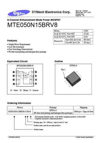
Spec. No. C033V8 Issued Date 2017.10.05 CYStech Electronics Corp. Revised Date Page No. 1/9 N-Channel Enhancement Mode Power MOSFET MTE050N15BRV8 BVDSS 150V ID @ TC=25 C, VGS=10V 12.4A ID @ TA=25 C, VGS=10V 4.3A 49.1m VGS=10V, ID=3.4A Features RDSON(TYP) 58.5m VGS=6V, ID=3.3A Single Drive Requirement Low On-resistance Fast Switchi
0.10. Size:333K cystek
mte50n15q8.pdf 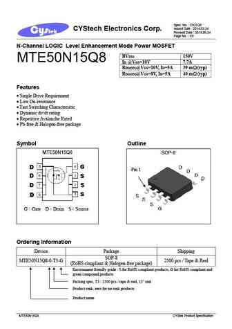
Spec. No. C931Q8 Issued Date 2014.03.24 CYStech Electronics Corp. Revised Date 2014.06.24 Page No. 1/9 N-Channel LOGIC Level Enhancement Mode Power MOSFET BVDSS 150V MTE50N15Q8 ID @VGS=10V 7.7A RDS(ON)@VGS=10V, ID=5A 39 m (typ) RDS(ON)@VGS=8V, ID=5A 40 m (typ) Features Single Drive Requirement Low On-resistance Fast Switching Characteristic
0.11. Size:858K cystek
mte050n15brh8.pdf 
Spec. No. C033H8 Issued Date 2017.11.15 CYStech Electronics Corp. Revised Date Page No. 1/11 N-Channel Enhancement Mode Power MOSFET MTE050N15BRH8 BVDSS 150V ID@VGS=10V, TC=25 C 16A ID@VGS=10V, TA=25 C 4.3A RDS(ON)@VGS=10V, ID=3.4A 49.1m (typ) Features RDS(ON)@VGS=6V, ID=3.3A 58.5 m (typ) Single Drive Requirement Low On-resistance Fast Switchi
0.12. Size:550K cystek
mtb050n15j3.pdf 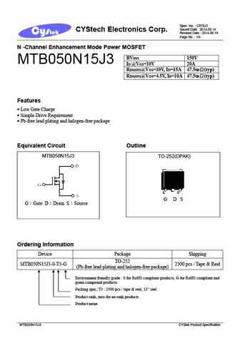
Spec. No. C979J3 Issued Date 2014.08.14 CYStech Electronics Corp. Revised Date 2014.08.18 Page No. 1/9 N -Channel Enhancement Mode Power MOSFET BVDSS 150V MTB050N15J3 ID @VGS=10V 20A RDS(ON)@VGS=10V, ID=15A 47.5m (typ) RDS(ON)@VGS=4.5V, ID=10A 47.5m (typ) Features Low Gate Charge Simple Drive Requirement Pb-free lead plating and halogen-free p
0.13. Size:1399K cn wxdh
dh50n15 dhf50n15 dhi50n15 dhe50n15.pdf 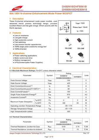
DH50N15/DHF50N15/ DHI50N15/DHE50N15 50A 150V N-channel Enhancement Mode Power MOSFET 1 Description These N-channel enhancement mode power mosfets. used 2 D V = 150V DSS advanced trench process technology design, provided excellent Rdson and low gate charge. Which accords with the R = 18m DS(on) (Type) G RoHS standard. 1 I = 50A 3 S D 2 Features Low on resistance Low
0.14. Size:4894K first semi
fir50n15pg.pdf 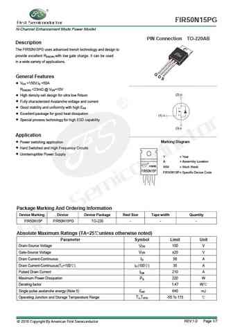
FIR50N15PG N-Channel Enhancement Mode Power Mosfet PIN Connection TO-220AB Description The FIR50N15PG uses advanced trench technology and design to provide excellent RDS(ON) with low gate charge. It can be used in a wide variety of applications. General Features VDS =150V,ID =50A RDS(ON)
0.15. Size:736K huashuo
hsp150n15.pdf 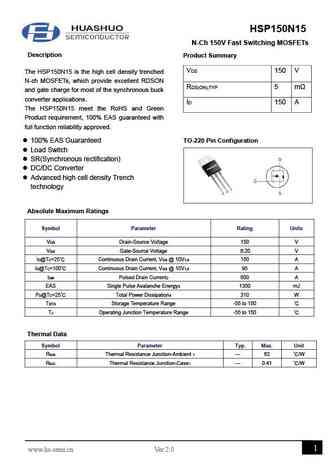
HSP150N15 N-Ch 150V Fast Switching MOSFETs Description Product Summary VDS 150 V The HSP150N15 is the high cell density trenched N-ch MOSFETs, which provide excellent RDSON RDS(ON),TYP 5 m and gate charge for most of the synchronous buck converter applications. ID 150 A The HSP150N15 meet the RoHS and Green Product requirement, 100% EAS guaranteed with full function
0.17. Size:900K cn hunteck
hgs650n15s.pdf 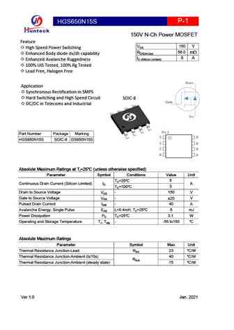
HGS650N15S P-1 150V N-Ch Power MOSFET Feature 150 V VDS High Speed Power Switching 58.0 RDS(on),typ mW Enhanced Body diode dv/dt capability 5 A ID (Sillicon Limited) Enhanced Avalanche Ruggedness 100% UIS Tested, 100% Rg Tested Lead Free, Halogen Free Drain Application Synchronous Rectification in SMPS Hard Switching and High Speed Circuit SOIC-8 G
0.18. Size:894K cn hunteck
hgd650n15s.pdf 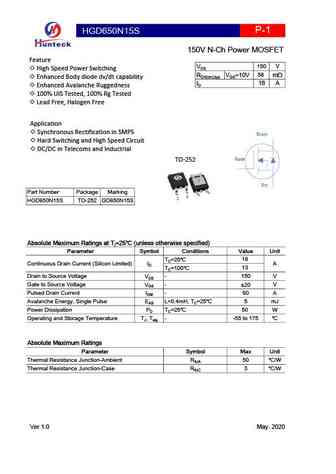
HGD650N15S P-1 150V N-Ch Power MOSFET Feature 150 V VDS High Speed Power Switching 58 RDS(on),typ VGS=10V mW Enhanced Body diode dv/dt capability 18 A ID Enhanced Avalanche Ruggedness 100% UIS Tested, 100% Rg Tested Lead Free, Halogen Free Application Synchronous Rectification in SMPS Drain Hard Switching and High Speed Circuit DC/DC in Telecoms
0.19. Size:900K cn hunteck
hgd650n15sl.pdf 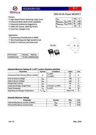
HGD650N15SL P-1 150V N-Ch Power MOSFET Feature 150 V VDS High Speed Power Switching, Logic Level 58 RDS(on),typ VGS=10V mW Enhanced Body diode dv/dt capability 66 RDS(on),typ VGS=4.5V mW Enhanced Avalanche Ruggedness 18 A ID 100% UIS Tested, 100% Rg Tested Lead Free, Halogen Free Application Synchronous Rectification in SMPS Drain Hard Switching an
0.20. Size:895K cn hunteck
hgd750n15ml hgi750n15ml.pdf 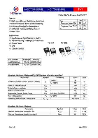
HGD750N15ML HGI750N15ML P-1 , 150V N-Ch Power MOSFET Feature 150 V VDS High Speed Power Switching, logic level 63 RDS(on),typ VGS=10V m Enhanced Body diode dv/dt capability 72 RDS(on),typ VGS=4.5V m Enhanced Avalanche Ruggedness 18 A ID 100% UIS Tested, 100% Rg Tested Lead Free Application Synchronous Rectification in SMPS Hard Switching and
0.21. Size:893K cn hunteck
hgn650n15sl.pdf 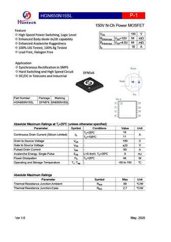
HGN650N15SL P-1 150V N-Ch Power MOSFET Feature 150 V VDS High Speed Power Switching, Logic Level 58 RDS(on),typ VGS=10V mW Enhanced Body diode dv/dt capability 66 RDS(on),typ VGS=4.5V mW Enhanced Avalanche Ruggedness 18 A ID 100% UIS Tested, 100% Rg Tested Lead Free, Halogen Free Application Synchronous Rectification in SMPS Drain Hard Switching an
0.22. Size:904K cn hunteck
hgs650n15sl.pdf 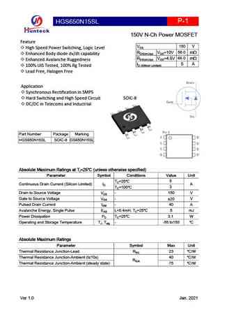
HGS650N15SL P-1 150V N-Ch Power MOSFET Feature 150 V VDS High Speed Power Switching, Logic Level 58.0 RDS(on),typ VGS=10V mW Enhanced Body diode dv/dt capability 66.0 RDS(on),typ VGS=4.5V mW Enhanced Avalanche Ruggedness 5 A ID (Sillicon Limited) 100% UIS Tested, 100% Rg Tested Lead Free, Halogen Free Drain Application Synchronous Rectification in SMPS
0.23. Size:906K cn hunteck
hgs750n15ml.pdf 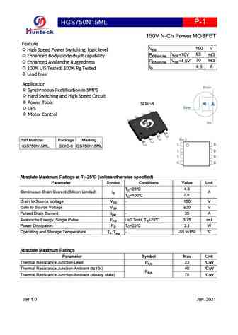
HGS750N15ML P-1 150V N-Ch Power MOSFET Feature 150 V VDS High Speed Power Switching, logic level 63 RDS(on),typ VGS=10V mW Enhanced Body diode dv/dt capability 70 RDS(on),typ VGS=4.5V mW Enhanced Avalanche Ruggedness 4.6 A ID 100% UIS Tested, 100% Rg Tested Lead Free Application Drain Synchronous Rectification in SMPS Hard Switching and High Speed
0.24. Size:892K cn hunteck
hgn650n15s.pdf 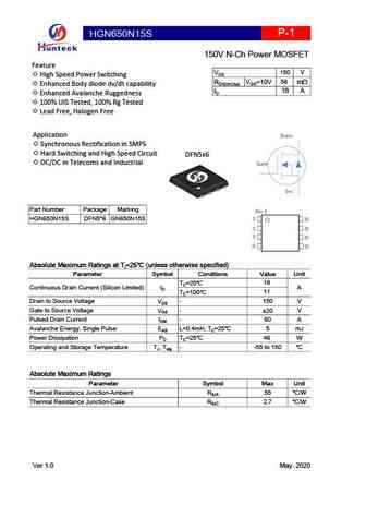
HGN650N15S P-1 150V N-Ch Power MOSFET Feature 150 V VDS High Speed Power Switching 58 RDS(on),typ VGS=10V mW Enhanced Body diode dv/dt capability 18 A ID Enhanced Avalanche Ruggedness 100% UIS Tested, 100% Rg Tested Lead Free, Halogen Free Application Drain Synchronous Rectification in SMPS Hard Switching and High Speed Circuit DFN5x6 DC/DC in T
0.26. Size:746K cn hmsemi
hms50n15ld.pdf 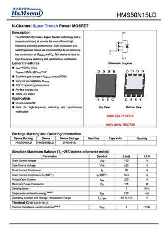
HMS50N15LD N-Channel Super Trench Power MOSFET Description The HMS50N15LD uses Super Trench technology that is uniquely optimized to provide the most efficient high frequency switching performance. Both conduction and switching power losses are minimized due to an extremely low combination of RDS(ON) and Qg. This device is ideal for high-frequency switching and synchronous recti
0.27. Size:575K cn hmsemi
hm50n15d.pdf 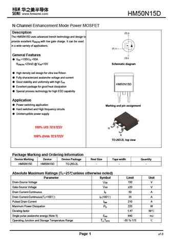
HM50N15 N-Channel Enhancement Mode Power MOSFET Description The HM50N15 uses advanced trench technology and design to provide excellent RDS(ON) with low gate charge. It can be used in a wide variety of applications. General Features VDS =150V,ID =50A RDS(ON)
0.28. Size:525K cn hmsemi
hm50n15.pdf 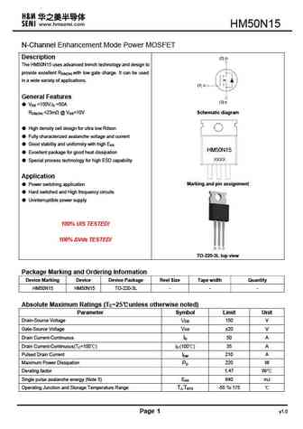
HM50N15 N-Channel Enhancement Mode Power MOSFET Description The HM50N15 uses advanced trench technology and design to provide excellent RDS(ON) with low gate charge. It can be used in a wide variety of applications. General Features VDS =150V,ID =50A RDS(ON)
Другие MOSFET... 2SK1917-M
, 2SK1938-01
, 2SK1939-01
, 2SK1982-01M
, 2SK2020-01MR
, 2SK2645
, 2SK2850
, 40N10
, IRF4905
, 60N05
, 60N05-16
, 60N06-18
, 60N10
, 6N70A
, 75N06
, 75N10
, 75NF75
.