60N10. Аналоги и основные параметры
Наименование производителя: 60N10
Тип транзистора: MOSFET
Полярность: N
Предельные значения
Pd ⓘ - Максимальная рассеиваемая мощность: 150 W
|Vds|ⓘ - Максимально допустимое напряжение сток-исток: 100 V
|Vgs|ⓘ - Максимально допустимое напряжение затвор-исток: 20 V
|Id| ⓘ - Максимально допустимый постоянный ток стока: 60 A
Tj ⓘ - Максимальная температура канала: 150 °C
Электрические характеристики
tr ⓘ - Время нарастания: 280 ns
RDSonⓘ - Сопротивление сток-исток открытого транзистора: 0.03 Ohm
Тип корпуса: TO-3PN
Аналог (замена) для 60N10
- подборⓘ MOSFET транзистора по параметрам
60N10 даташит
60n10 60n10f 60n10b 60n10d 60n10i 60n10e.pdf
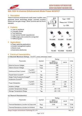
60N10/60N10F/60N10B 60N10D/60N10I/60N10E 59A 100V N-channel Enhancement Mode Power MOSFET 1 Description These N-channel enhancement mode power mosfets used 2 D V = 100V DSS advanced trench technology design, provided excellent Rdson and low gate charge. Which accords with the RoHS G R = 13.0m DS(on) (TYP) standard. 1 3 S I = 59A D 2 Features Low on resistance Low g
60n10.pdf
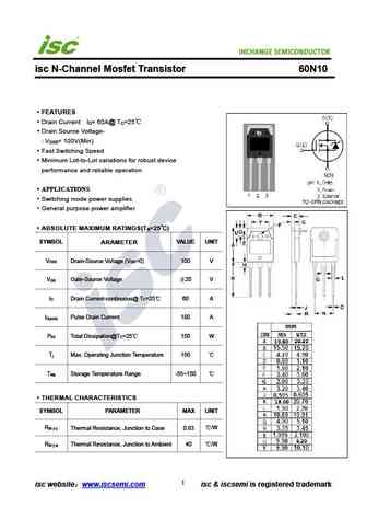
INCHANGE Semiconductor isc N-Channel Mosfet Transistor 60N10 FEATURES Drain Current I = 60A@ T =25 D C Drain Source Voltage- V = 100V(Min) DSS Fast Switching Speed Minimum Lot-to-Lot variations for robust device performance and reliable operation APPLICATIONS Switching mode power supplies General purpose power amplifier ABSOLUTE MAXIMUM RATINGS(T =25 ) a
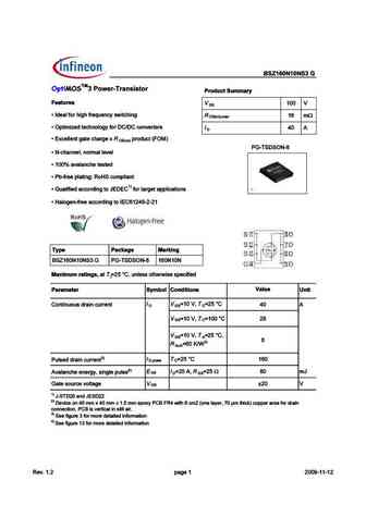
bsz160n10ns3g.pdf
MOSFET Metal Oxide Semiconductor Field Effect Transistor OptiMOS Power-Transistor, 100V OptiMOS 3 Power Transistor BSZ160N10NS3 Data Sheet Rev. 2.1 Final Power Management & Multimarket BSZ160N10NS3 G OptiMOSTM3 Power-Transistor Product Summary Features VDS 100 V Ideal for high frequency switching RDS(on),max 16 mW Optimized technology for DC/DC converters ID
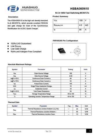
hsba060n10.pdf
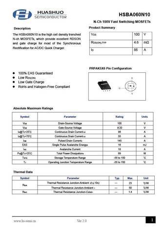
HSBA060N10 N-Ch 100V Fast Switching MOSFETs Product Summary Description The HSBA060N10 is the high cell density trenched VDS 100 V N-ch MOSFETs, which provide excellent RDSON RDS(ON),TYP 4.6 m and gate charge for most of the Synchronous Rectification for AC/DC Quick Charger. ID 86 A PRPAK5X6 Pin Configuration 100% EAS Guaranteed Low RDS(ON) Low Gate Charg
sth60n10.pdf
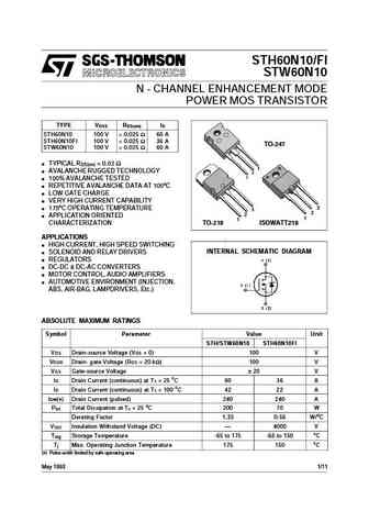
STH60N10/FI STW60N10 N - CHANNEL ENHANCEMENT MODE POWER MOS TRANSISTOR TYPE VDSS RDS(on) ID STH60N10 100 V
stl60n10f7.pdf
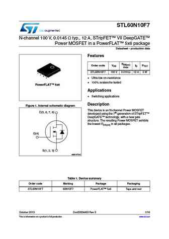
STL60N10F7 N-channel 100 V, 0.0145 typ., 12 A, STripFET VII DeepGATE Power MOSFET in a PowerFLAT 5x6 package Datasheet - production data Features RDS(on) Order code VDS max ID PTOT STL60N10F7 100 V 0.018 12 A 5 W 1 2 3 4 Ultra low on-resistance 100% avalanche tested PowerFLAT 5x6 Applications Switching applications Description Figure 1. Intern
stw60n10.pdf
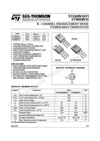
STH60N10/FI STW60N10 N - CHANNEL ENHANCEMENT MODE POWER MOS TRANSISTOR TYPE VDSS RDS(on) ID STH60N10 100 V
fgl60n100bntd.pdf
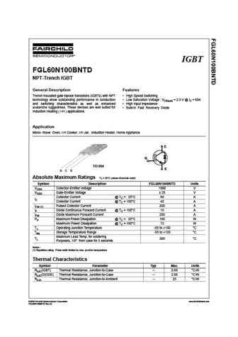
IGBT FGL60N100BNTD NPT-Trench IGBT General Description Features Trench insulated gate bipolar transistors (IGBTs) with NPT High Speed Switching technology show outstanding performance in conduction Low Saturation Voltage VCE(sat) = 2.5 V @ IC = 60A and switching characteristics as well as enhanced High Input Impedance avalanche ruggedness. These devices are well suited for
sup60n10.pdf
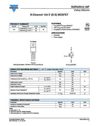
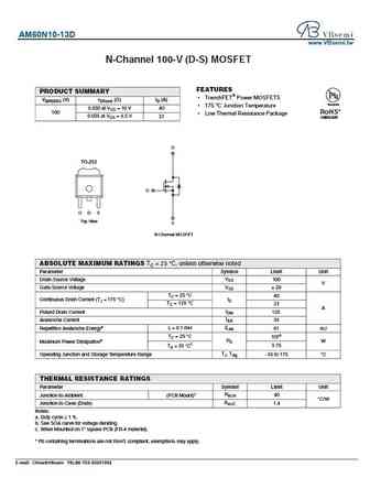
SUP60N10-18P Vishay Siliconix N-Channel 100-V (D-S) MOSFET FEATURES PRODUCT SUMMARY TrenchFET Power MOSFET VDS (V) RDS(on) ( ) ID (A) Qg (Typ.) 100 % Rg and UIS Tested 0.0183 at VGS = 10 V 60 100 48 Compliant to RoHS Directive 2002/95/EC 0.023 at VGS = 8.0 V 53 APPLICATIONS Industrial Power Supply TO-220AB D G G D S S Top View Ordering Inf
sum60n10-17.pdf
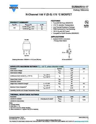
SUM60N10-17 Vishay Siliconix N-Channel 100 V (D-S) 175 C MOSFET FEATURES PRODUCT SUMMARY TrenchFET Power MOSFETS VDS (V) RDS(on) ( )ID (A) 175 C Junction Temperature 0.0165 at VGS = 10 V 60 Low Thermal Resistance Package 100 0.0190 at VGS = 6 V 56 PWM Optimized for Fast Switching 100 % Rg and UIS Tested Compliant to RoHS Directive 2002/
sup60n10-16l.pdf
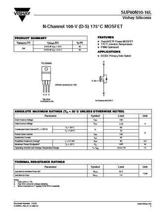
SUP60N10-16L Vishay Siliconix N-Channel 100-V (D-S) 175_C MOSFET FEATURES PRODUCT SUMMARY D TrenchFETr Power MOSFET V(BR)DSS (V) rDS(on) (W) ID (A) D 175_C Junction Temperature 0.016 @ VGS = 10 V 60 D PWM Optimized 100 100 0.018 @ VGS = 4.5 V 56 APPLICATIONS D DC/DC Primary Side Switch D TO-220AB G DRAIN connected to TAB G D S S Top View N-Channel MOSFET SUP60N10-16L ABS
sup60n10-18p.pdf

SUP60N10-18P Vishay Siliconix N-Channel 100-V (D-S) MOSFET FEATURES PRODUCT SUMMARY TrenchFET Power MOSFET VDS (V) RDS(on) ( ) ID (A) Qg (Typ.) 100 % Rg and UIS Tested 0.0183 at VGS = 10 V 60 100 48 Compliant to RoHS Directive 2002/95/EC 0.023 at VGS = 8.0 V 53 APPLICATIONS Industrial Power Supply TO-220AB D G G D S S Top View Ordering Inf
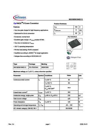
bsc160n10ns3 bsc160n10ns3g.pdf
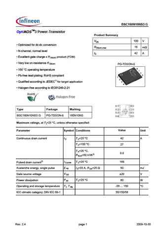
Type BSC160N10NS3 G TM 3 Power-Transistor Product Summary VDS 100 V 9 .1)+ )7%$ &-/ $# $# # -,3%/0)-, RDS(on),max 16 m 9 # (!,,%* ,-/+ !* *%3%* ID 42 A 9 5# %**%,1 '!1% # (!/'% 5 R product (FOM) DS(on) 9 %/6 *-4 -, /%0)01!,# % R DS(on) PG-TDSON-8 9 8 -.%/!1),' 1%+ .%/!12/% 9 " &/%% *%!$ .*!1),' - # -+ .*)!,1 1) 9 2!*)&)%$ !# # -/$),' 1- for target application 9 !*-'%, &/%%
ipd60n10s4l-12.pdf
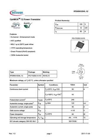
IPD60N10S4L-12 OptiMOSTM-T2 Power-Transistor Product Summary V 100 V DS R 12 mW DS(on),max I 60 A D Features N-channel - Enhancement mode PG-TO252-3-313 AEC qualified TAB MSL1 up to 260 C peak reflow 175 C operating temperature 1 3 Green Product (RoHS compliant) 100% Avalanche tested Type Package Marking IPD60N10S4L-12 PG-TO252-3-313 4N10L12 Maxi
ipd60n10s4-12.pdf
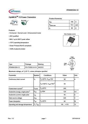
IPD60N10S4-12 OptiMOSTM-T2 Power-Transistor Product Summary VDS 100 V RDS(on),max 12.2 mW ID 60 A Features N-channel - Normal Level - Enhancement mode PG-TO252-3-313 AEC qualified TAB MSL1 up to 260 C peak reflow 175 C operating temperature 1 3 Green Product (RoHS compliant) 100% Avalanche tested Drain pin 2/Tab Gate Type Package Marking pin 1 IP
bsz160n10n3sg.pdf
%* ! !% #;B 1= &=- >5>?;= #=;0@/? %@99-=D Features 1 D Q #4513I CG9D389>7 1 m D n) m x Q ( @D9=9J54 D538>?F5BD5BC 4 D Q H35>5?B=1
bsz160n10ns3.pdf

MOSFET Metal Oxide Semiconductor Field Effect Transistor OptiMOS Power-Transistor, 100V OptiMOS 3 Power Transistor BSZ160N10NS3 Data Sheet Rev. 2.1 Final Power Management & Multimarket BSZ160N10NS3 G OptiMOSTM3 Power-Transistor Product Summary Features VDS 100 V Ideal for high frequency switching RDS(on),max 16 mW Optimized technology for DC/DC converters ID
ixta160n10t7.pdf
Preliminary Technical Information VDSS = 100 V IXTA160N10T7 TrenchMVTM ID25 = 160 A Power MOSFET RDS(on) 7.0 m N-Channel Enhancement Mode Avalanche Rated Symbol Test Conditions Maximum Ratings TO-263 (7-lead) (IXTA..7) VDSS TJ = 25 C to 175 C 100 V VDGR TJ = 25 C to 175 C; RGS = 1 M 100 V VGSM Transient 30 V 1 ID25 TC = 25 C 160 A
ixth160n10t ixtq160n10t.pdf
Preliminary Technical Information IXTH160N10T VDSS = 100 V TrenchMVTM IXTQ160N10T ID25 = 160 A Power MOSFET RDS(on) 7.0 m N-Channel Enhancement Mode TO-247 (IXTH) Avalanche Rated Symbol Test Conditions Maximum Ratings G (TAB) D S VDSS TJ = 25 C to 175 C 100 V VDGR TJ = 25 C to 175 C; RGS = 1 M 100 V VGSM Transient 30 V TO-3P (IXTQ)
ixta60n10t ixtp60n10t.pdf
TrenchTM VDSS = 100V IXTA60N10T ID25 = 60A Power MOSFET IXTP60N10T RDS(on) 18m N-Channel Enhancement Mode TO-263 Avalanche Rated (IXTA) G S D (Tab) Symbol Test Conditions Maximum Ratings TO-220 VDSS TJ = 25 C to 175 C 100 V (IXTP) VDGR TJ = 25 C to 175 C, RGS = 1M 100 V VGSS Continuous 20 V VGSM Transient 30 V G
ixta160n10t ixtp160n10t.pdf
Preliminary Technical Information IXTA160N10T VDSS = 100 V TrenchMVTM IXTP160N10T ID25 = 160 A Power MOSFET RDS(on) 7.0 m N-Channel Enhancement Mode Avalanche Rated TO-263 (IXTA) G S Symbol Test Conditions Maximum Ratings (TAB) VDSS TJ = 25 C to 175 C 100 V TO-220 (IXTP) VDGR TJ = 25 C to 175 C; RGS = 1 M 100 V VGSM Transient 30 V
ixtc160n10t.pdf
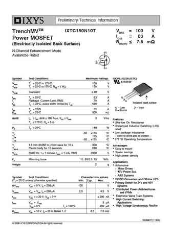
Preliminary Technical Information IXTC160N10T VDSS = 100 V TrenchMVTM ID25 = 83 A Power MOSFET RDS(on) 7.5 m (Electrically Isolated Back Surface) N-Channel Enhancement Mode Avalanche Rated Symbol Test Conditions Maximum Ratings ISOPLUS220 (IXTC) E153432 VDSS TJ = 25 C to 175 C 100 V VDGR TJ = 25 C to 175 C; RGS = 1 M 100 V VGSM Transient
mcb160n10y.pdf
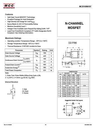
MCB160N10Y Features Split Gate Trench MOSFET Technology Excellent Package for Heat Dissipation High Density Cell Design for Low RDS(on) Epoxy Meets UL 94 V-0 Flammability Rating N-CHANNEL Moisture Sensitivity Level 1 MOSFET Halogen Free Available Upon Request By Adding Suffix "-HF" Lead Free Finish/RoHS Compliant ("P" Suffix Designates RoHS Compliant. See O
om60n10sc.pdf
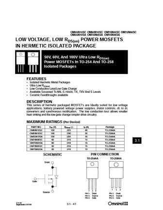
OM55N10SC OM60N10SC OM75N05SC OM75N06SC OM55N10SA OM75N05SA OM75N06SA LOW VOLTAGE, LOW RDS(on) POWER MOSFETS IN HERMETIC ISOLATED PACKAGE 50V, 60V, And 100V Ultra Low RDS(on) Power MOSFETs In TO-254 And TO-258 Isolated Packages FEATURES Isolated Hermetic Metal Packages Ultra Low RDS(on) Low Conductive Loss/Low Gate Charge Available Screened To MIL-S-19500, TX, TXV And
fgl60n100bntd.pdf

Is Now Part of To learn more about ON Semiconductor, please visit our website at www.onsemi.com Please note As part of the Fairchild Semiconductor integration, some of the Fairchild orderable part numbers will need to change in order to meet ON Semiconductor s system requirements. Since the ON Semiconductor product management systems do not have the ability to manage part nomenclatur
fdbl0260n100.pdf

Is Now Part of To learn more about ON Semiconductor, please visit our website at www.onsemi.com Please note As part of the Fairchild Semiconductor integration, some of the Fairchild orderable part numbers will need to change in order to meet ON Semiconductor s system requirements. Since the ON Semiconductor product management systems do not have the ability to manage part nomenclatur
fdb0260n1007l.pdf

Is Now Part of To learn more about ON Semiconductor, please visit our website at www.onsemi.com Please note As part of the Fairchild Semiconductor integration, some of the Fairchild orderable part numbers will need to change in order to meet ON Semiconductor s system requirements. Since the ON Semiconductor product management systems do not have the ability to manage part nomenclatur
utt60n10.pdf
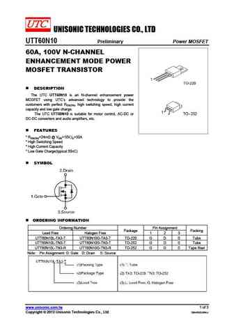
UNISONIC TECHNOLOGIES CO., LTD UTT60N10 Preliminary Power MOSFET 60A, 100V N-CHANNEL ENHANCEMENT MODE POWER MOSFET TRANSISTOR DESCRIPTION The UTC UTT60N10 is an N-channel enhancement power MOSFET using UTC s advanced technology to provide the customers with perfect RDS(ON), high switching speed, high current capacity and low gate charge. The UTC UTT60N10 is suitable f
ssrf60n10.pdf
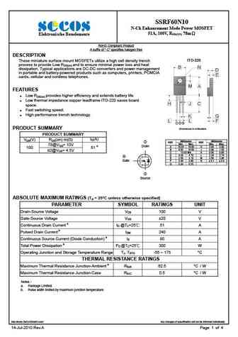
SSRF60N10 N-Ch Enhancement Mode Power MOSFET 51A, 100V, RDS(ON) 78m Elektronische Bauelemente RoHS Compliant Product A suffix of -C specifies halogen free DESCRIPTION These miniature surface mount MOSFETs utilize a high cell density trench ITO-220 process to provide Low RDS(on) and to ensure minimal power loss and heat B N dissipation. Typical applications are DC-DC co
tsm160n10cz.pdf
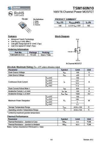
TSM160N10 100V N-Channel Power MOSFET TO-220 Pin Definition PRODUCT SUMMARY 1. Gate VDS (V) RDS(on)(m ) ID (A) 2. Drain 3. Source 100 5.5 @ VGS =10V 160 Features Block Diagram Advanced Trench Technology Low RDS(ON) 5.5m (Max.) Low gate charge typical @ 154nC (Typ.) Low Crss typical @ 300pF (Typ.) Ordering Information Part No. Package Packing
tsg60n100.pdf

TSG60N100CE N-Channel IGBT with FRD. TO-264 Pin Definition PRODUCT SUMMARY 1. Gate 2. Collector VCES (V) VGES (V) IC (A) 3. Emitter 1000 20 60 General Description The TSG60N100CE using proprietary trench design and advanced NPT technology, the 1000V NPT IGBT offers superior conduction and switching performances, high avalanche ruggedness and easy parallel operation.
tsg60n100ce.pdf
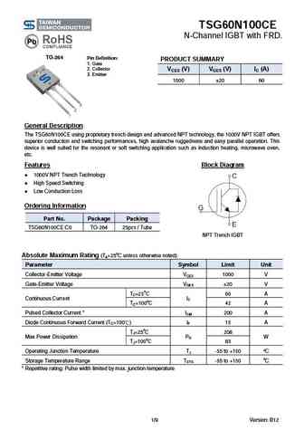
TSG60N100CE N-Channel IGBT with FRD. TO-264 Pin Definition PRODUCT SUMMARY 1. Gate 2. Collector VCES (V) VGES (V) IC (A) 3. Emitter 1000 20 60 General Description The TSG60N100CE using proprietary trench design and advanced NPT technology, the 1000V NPT IGBT offers superior conduction and switching performances, high avalanche ruggedness and easy parallel operation.
cep60n10 ceb60n10.pdf
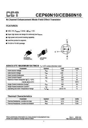
CEP60N10/CEB60N10 N-Channel Enhancement Mode Field Effect Transistor FEATURES 100V, 57A, RDS(ON) = 24m @VGS = 10V. Super high dense cell design for extremely low RDS(ON). High power and current handing capability. D Lead free product is acquired. TO-220 & TO-263 package. G CEB SERIES CEP SERIES S TO-263(DD-PAK) TO-220 ABSOLUTE MAXIMUM RATINGS Tc = 25 C unless otherwise noted
am60n10-70p.pdf
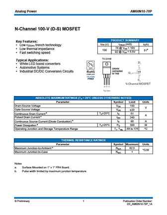
Analog Power AM60N10-70P N-Channel 100-V (D-S) MOSFET PRODUCT SUMMARY Key Features rDS(on) (m ) VDS (V) ID(A) Low r trench technology DS(on) 78 @ VGS = 10V Low thermal impedance 100 51a 92 @ VGS = 5.5V Fast switching speed Typical Applications White LED boost converters Automotive Systems DRAIN connected Industrial DC/DC Conversion Circuits
am60n10-13d.pdf
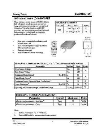
Analog Power AM60N10-13D N-Channel 100-V (D-S) MOSFET These miniature surface mount MOSFETs utilize a PRODUCT SUMMARY high cell density trench process to provide low VDS (V) rDS(on) m( ) ID (A) rDS(on) and to ensure minimal power loss and heat dissipation. Typical applications are DC-DC 13 @ VGS = 10V 51 converters and power management in portable and 100 14 @ VGS = 5.5V 49 bat
am60n10-70pcfm.pdf
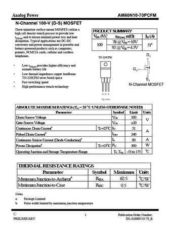
Analog Power AM60N10-70PCFM N-Channel 100-V (D-S) MOSFET These miniature surface mount MOSFETs utilize a PRODUCT SUMMARY high cell density trench process to provide low VDS (V) rDS(on) m( ) ID (A) rDS(on) and to ensure minimal power loss and heat dissipation. Typical applications are DC-DC 78 @ VGS = 10V converters and power management in portable and 100 51a 92 @ VGS = 4.5V
jcs60n10i.pdf
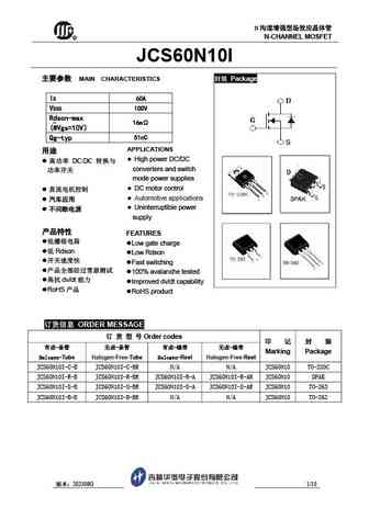
N N-CHANNEL MOSFET JCS60N10I MAIN CHARACTERISTICS Package ID 60A VDSS 100V Rdson-max - 16m (@Vgs=10V Qg-typ 51nC APPLICATIONS High power DC/DC DC/DC converters and switch mode power supplies DC motor control Automotive app
gt060n10t gt060n10m.pdf
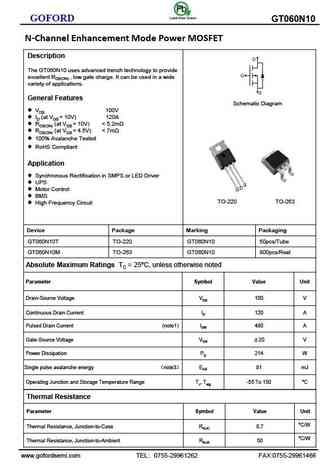
GOFORD GT060N10 N-Channel Enhancement Mode Power MOSFET Description The GT060N10 uses advanced trench technology to provide excellent RDS(ON) , low gate charge. It can be used in a wide variety of applications. General Features Schematic Diagram VDS 100V ID (at VGS = 10V) 120A RDS(ON) (at VGS = 10V)
crst060n10n crss057n10n.pdf
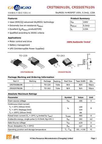
CRST060N10N, CRSS057N10N ( ) SkyMOS1 N-MOSFET 100V, 5.3m , 120A Features Product Summary VDS Uses CRM(CQ) advanced SkyMOS1 technology 100V Extremely low on-resistance RDS(on) RDS(on) 5.3m Excellent QgxRDS(on) product(FOM) ID 120A Qualified according to JEDEC criteria Applications Motor control and drive 100% Avalanche Tested
dhs160n100b dhs160n100d.pdf
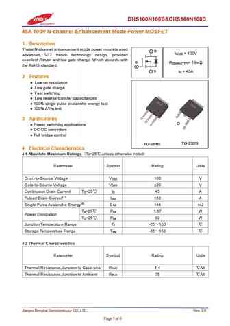
DHS160N100B&DHS160N100D 45A 100V N-channel Enhancement Mode Power MOSFET 1 Description These N-channel enhancement mode power mosfets used 2 D V = 100V DSS advanced SGT trench technology design, provided excellent Rdson and low gate charge. Which accords with G R = 18m DS(on) (TYP) the RoHS standard. 1 3 S I = 45A D 2 Features Low on resistance Low gate charge
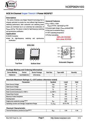
ncep060n10f.pdf
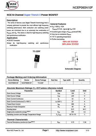
NCEP060N10F NCE N-Channel Super Trench II Power MOSFET Description The series of devices uses Super Trench II technology that is General Features uniquely optimized to provide the most efficient high frequency VDS =100V,ID =52A switching performance. Both conduction and switching power RDS(ON)=6.7m , typical @ VGS=10V losses are minimized due to an extremely low combina
ncep060n10 ncep060n10d.pdf

NCEP060N10, NCEP060N10D NCE N-Channel Super Trench II Power MOSFET Description The series of devices uses Super Trench II technology that is General Features uniquely optimized to provide the most efficient high frequency VDS =100V,ID =100A switching performance. Both conduction and switching power RDS(ON)=5.6m , typical (TO-220)@ VGS=10V losses are minimized due to an ex
ncep060n10g.pdf
NCEP060N10G NCE N-Channel Super Trench II Power MOSFET Description The series of devices uses Super Trench II technology that is General Features uniquely optimized to provide the most efficient high frequency VDS =100V,ID =100A switching performance. Both conduction and switching power RDS(ON)=5.4m , typical @ VGS=10V losses are minimized due to an extremely low combin
ncep060n10d.pdf

NCEP060N10, NCEP060N10D NCE N-Channel Super Trench II Power MOSFET Description The series of devices uses Super Trench II technology that is General Features uniquely optimized to provide the most efficient high frequency VDS =100V,ID =100A switching performance. Both conduction and switching power RDS(ON)=5.6m , typical (TO-220)@ VGS=10V losses are minimized due to an ex
ncep060n10.pdf
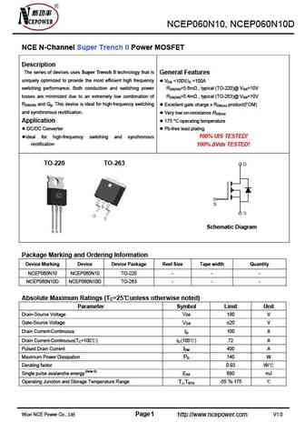
NCEP060N10, NCEP060N10D NCE N-Channel Super Trench II Power MOSFET Description The series of devices uses Super Trench II technology that is General Features uniquely optimized to provide the most efficient high frequency VDS =100V,ID =100A switching performance. Both conduction and switching power RDS(ON)=5.6m , typical (TO-220)@ VGS=10V losses are minimized due to an ex
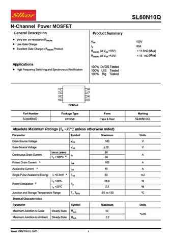
sl60n10q.pdf
SL60N10Q N-Channel Power MOSFET General Description Product Summary Very low on-resistance RDS(ON) VDS 100V Low Gate Charge ID 60A Excellent Gate Charge x RDS(ON) Product RDS(ON) (at VGS =10V)
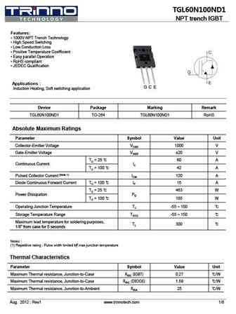
tgl60n100nd1.pdf
TGL60N100ND1 NPT trench IGBT Features 1000V NPT Trench Technology High Speed Switching Low Conduction Loss Positive Temperature Coefficient Easy parallel Operation RoHS compliant JEDEC Qualification Applications G C E Induction Heating, Soft switching application Device Package Marking Remark TGL60N100ND1 TO-264 TGL60N100ND1 RoHS Absolute Maximum Ra
wmb060n10lgs.pdf
WMB060N10LGS 100V N-Channel Enhancement Mode Power MOSFET Description D D D D WMB060N10LGS uses Wayon's advanced power trench MOSFET D D D D technology that has been especially tailored to minimize the on-state G ss resistance and yet maintain superior switching performance. This s ss G s device is well suited for high efficiency fast switching applications. PDFN5060-8L
wml060n10hgs.pdf
WML060N10HGS 100V N-Channel Enhancement Mode Power MOSFET Description WML060N10HGS uses Wayon's advanced power trench MOSFET technology that has been especially tailored to minimize the on-state resistance and yet maintain superior switching performance. This device GDS is well suited for high efficiency fast switching applications. TO-220F Features V = 100V, I = 65A DS
wmb060n10hgs.pdf
WMB060N10HGS 100V N-Channel Enhancement Mode Power MOSFET Description D D D D WMB060N10HGS uses Wayon's advanced power trench MOSFET D D D D technology that has been especially tailored to minimize the on-state G ss resistance and yet maintain superior switching performance. This s ss G s device is well suited for high efficiency fast switching applications. PDFN5060-8L
wmo060n10hgs.pdf
WMO060N10HGS 100V N-Channel Enhancement Mode Power MOSFET Description WMO060N10HGS uses Wayon's advanced power trench MOSFET technology that has been especially tailored to minimize the on-state D resistance and yet maintain superior switching performance. This S device is well suited for high efficiency fast switching applications. G TO-252 Features V = 100V, I = 105A
wmk060n10lgs.pdf
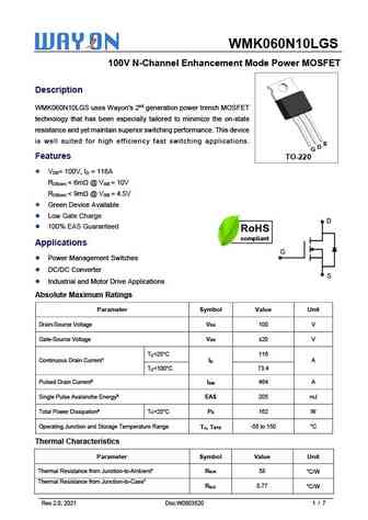
WMK060N10LGS 100V N-Channel Enhancement Mode Power MOSFET Description WMK060N10LGS uses Wayon's 2nd generation power trench MOSFET technology that has been especially tailored to minimize the on-state resistance and yet maintain superior switching performance. This device is well suited for high efficiency fast switching applications. S D G Features TO-220 V = 100V, I =
dami160n100.pdf
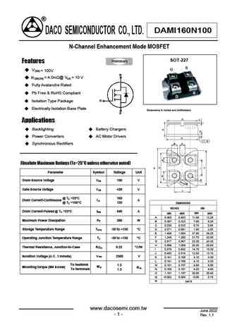
DAMI160N100 DACO SEMICONDUCTOR CO., LTD. N-Channel Enhancement Mode MOSFET SOT-227 Preliminary Features S G VDSS = 100V RDS(ON)
dami560n100.pdf
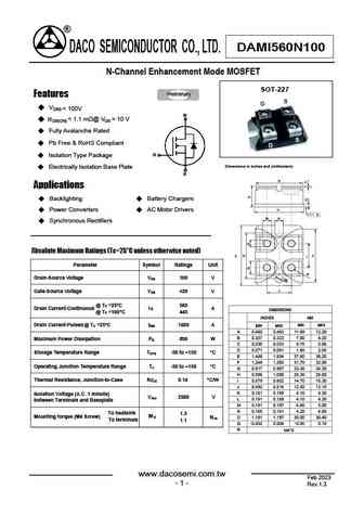
DAMI560N100 DACO SEMICONDUCTOR CO., LTD. N-Channel Enhancement Mode MOSFET SOT-227 Preliminary Features S G VDSS = 100V RDS(ON)
damh560n100.pdf
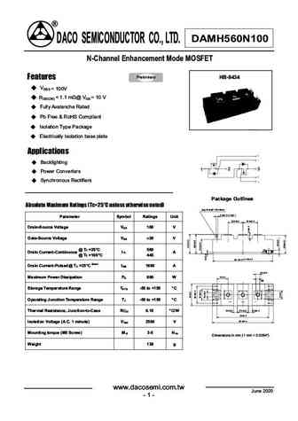
DAMH560N100 DACO SEMICONDUCTOR CO., LTD. N-Channel Enhancement Mode MOSFET Preliminary HB-9434 Features VDSS = 100V RDS(ON)
hsba060n10.pdf
HSBA060N10 N-Ch 100V Fast Switching MOSFETs Product Summary Description The HSBA060N10 is the high cell density trenched VDS 100 V N-ch MOSFETs, which provide excellent RDSON RDS(ON),TYP 4.6 m and gate charge for most of the Synchronous Rectification for AC/DC Quick Charger. ID 86 A PRPAK5X6 Pin Configuration 100% EAS Guaranteed Low RDS(ON) Low Gate Charg
htd360n10.pdf
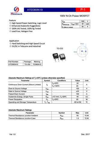
HTD360N10 P-1 100V N-Ch Power MOSFET Feature 100 V VDS High Speed Power Switching, Logic Level 32 RDS(on),typ VGS=10V m Enhanced Avalanche Ruggedness 30 A ID (Sillicon Limited) 100% UIS Tested, 100% Rg Tested Lead Free, Halogen Free Application Hard Switching and High Speed Circuit Drain DC/DC in Telecoms and Inductrial TO-252 Gate 2 Src 3 1 Part
wsd60n10gdn56.pdf
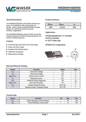
WSD60N10GDN56 N-Ch MOSFET General Description Product Summery The WSD60N10GDN56 is the highest performance BVDSS RDSON ID trench N-Ch MOSFET with extreme high cell density , which provide excellent RDSON and gate 100V 8.5m 60A charge for most of the synchronous buck converter applications . Applications The WSD60N10GDN56 meet the RoHS and Green Power Management in TV C
sum60n10-17.pdf
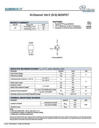
SUM60N10-17 www.VBsemi.tw N-Channel 100-V (D-S) MOSFET FEATURES PRODUCT SUMMARY TrenchFET Power MOSFET VDS (V) RDS(on) ( )ID (A) 175 C Maximum Junction Temperature 0.010 at VGS = 10 V 100 100 Compliant to RoHS Directive 2002/95/EC 0.023 at VGS = 4.5 V 85 D TO-263 G G D S Top View S N-Channel MOSFET ABSOLUTE MAXIMUM RATINGS TA = 25 C, unless otherw
am60n10-13d.pdf
AM60N10-13D www.VBsemi.tw N-Channel 100-V (D-S) MOSFET FEATURES PRODUCT SUMMARY TrenchFET Power MOSFETS V(BR)DSS (V) rDS(on) ( )ID (A) Available 175 C Junction Temperature 0.030 at VGS = 10 V 40 RoHS* 100 Low Thermal Resistance Package 0.035 at VGS = 4.5 V 37 COMPLIANT D TO-252 G G D S Top View S N-Channel MOSFET ABSOLUTE MAXIMUM RATINGS TC = 25 C, un
am60n10-70pc.pdf
AM60N10-70PC www.VBsemi.tw N-Channel 100-V (D-S) MOSFET FEATURES PRODUCT SUMMARY TrenchFET Power MOSFET V(BR)DSS (V) rDS(on) ( )ID (A) 175 C Junction Temperature RoHS 0.034 at VGS = 10 V 100 50a COMPLIANT Low Thermal Resistance Package 100 % Rg Tested APPLICATIONS Isolated DC/DC Converters D TO-220 FULLPAK G S S D G N-Channel MOSFET ABSOLUTE M
tmp160n10a.pdf
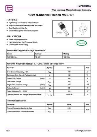
TMP160N10A Wuxi Unigroup Microelectronics Company 100V N-Channel Trench MOSFET FEATURES High Density Cell Design for Ultra Low Rdson Fully Characterized Avalanche Voltage and Current Good Stability with High EAS Excellent Package for Good Heat Dissipation APPLICATIONS Power Switching Application Hard Switched and High Frequency Circuits Uninter
s60n10m.pdf
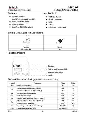
S60N10M SI-TECH SEMICONDUCTOR CO.,LTD N-Channel Power MOSFET Features Applications V =60V,I =100A DS D DC Motor Control Rds(on)(typ)=4.8m @Vgs=10V DC-DC Converters 100% Avalanche Tested BMS 100% Rg Tested SMPS Lead-Free (RoHS Compliant) Automotive Environment Internal Circuit and Pin Description D D G G S S Package
hms60n10d.pdf
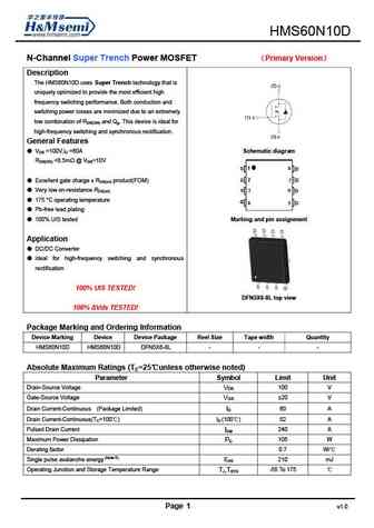
HMS60N10D N-Channel Super Trench Power MOSFET Primary Version Description The HMS60N10D uses Super Trench technology that is uniquely optimized to provide the most efficient high frequency switching performance. Both conduction and switching power losses are minimized due to an extremely low combination of RDS(ON) and Qg. This device is ideal for high-frequency switching an
hm60n10d.pdf
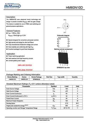
HM60N10D Description The HM60N10D uses advanced trench technology and design to provide excellent RDS(ON) with low gate charge. This device is suitable for use in PWM, load switching and general purpose applications. General Features VDS = 100V,ID =60A RDS(ON)
sfp60n100 sfb60n100 sfp350n100c2 sfb347n100c2.pdf
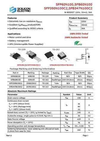
SFP60N100,SFB60N100 SFP350N100C2,SFB347N100C2 N-MOSFET 100V, 30m , 36A Features Product Summary Extremely low on-resistance RDS(on) VDS 100V Excellent QgxRDS(on) product(FOM) RDS(on) typ. 30m Qualified according to JEDEC criteria ID 36A Applications 100% DVDS Tested Motor control and drive 100% Avalanche Tested Battery management UPS (Uninterrupible
mdt60n10d.pdf
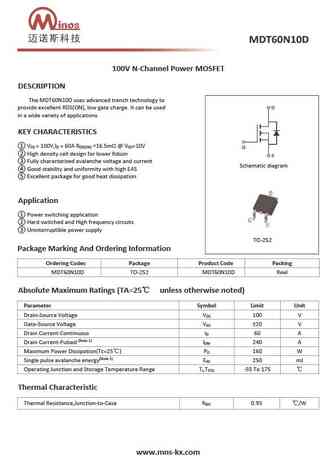
100V N-Channel Power MOSFET DESCRIPTION The MDT60N10D uses advanced trench technology to provide excellent RDS(ON), low gate charge. It can be used in a wide variety of applications. KEY CHARACTERISTICS V = 100V,I = 60A R
mpg60n10p mdt60n10d.pdf

DESCRIPTION The MPG60N10P uses advanced trench technology to provide excellent RDS(ON), low gate charge. It can be used in a wide variety of applications. Application Power switching application Hard switched and High frequency circuits Uninterruptible power supply Schematic diagram KEY CHARACTERISTICS V = 100V,I = 60A DS D R
ixta60n10t.pdf
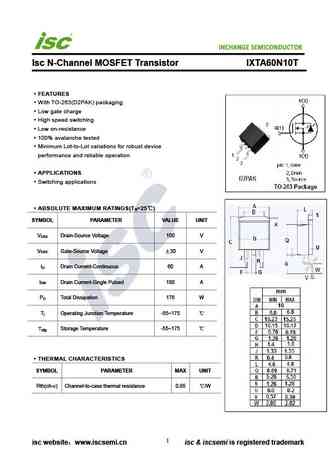
INCHANGE Semiconductor Isc N-Channel MOSFET Transistor IXTA60N10T FEATURES With TO-263(D2PAK) packaging Low gate charge High speed switching Low on-resistance 100% avalanche tested Minimum Lot-to-Lot variations for robust device performance and reliable operation APPLICATIONS Switching applications ABSOLUTE MAXIMUM RATINGS(T =25 ) a SYMBOL PARAMETER VALUE UNI
apg60n10p apg60n10t.pdf
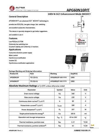
APG60N10PIT 100V N-SGT Enhancement Mode MOSFET General Description APG60N10P/T use advanced SGT MOSFET technology to provide low RDS(ON), low gate charge, fast switching and excellent avalanche characteristics. This device is specially designed to get better ruggedness and suitable to use in Features Low RDS(on) & FOM Extremely low switching loss Excellent stability and u
ap160n10p ap160n10t.pdf

AP160N10PIT 100V N-Channel Enhancement Mode MOSFET Description The AP160N10P/T uses advanced trench technology to provide excellent R , low gate charge and DS(ON) operation with gate voltages as low as 10V. This device is suitable for use as a Battery protection or in other Switching application. General Features V =100V I =160A DS D R
apg60n10nf.pdf
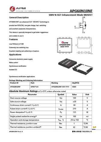
APG60N10NF 100V N-SGT Enhancement Mode MOSFET General Description APG60N10NF use advanced SGT MOSFET technology to provide low RDS(ON), low gate charge, fast switching and excellent avalanche characteristics. This device is specially designed to get better ruggedness and suitable to use in Features Low RDS(on) & FOM Extremely low switching loss Excellent stability and uni
apg60n10s.pdf
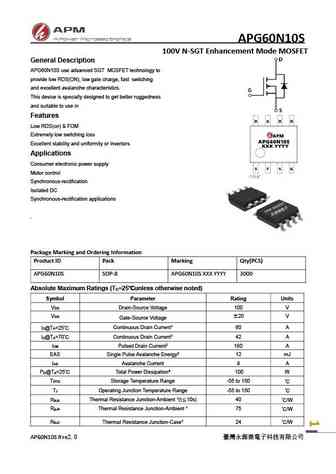
APG60N10S 100V N-SGT Enhancement Mode MOSFET General Description APG60N10S use advanced SGT MOSFET technology to provide low RDS(ON), low gate charge, fast switching and excellent avalanche characteristics. This device is specially designed to get better ruggedness and suitable to use in Features Low RDS(on) & FOM Extremely low switching loss Excellent stability and unifo
apg60n10d.pdf
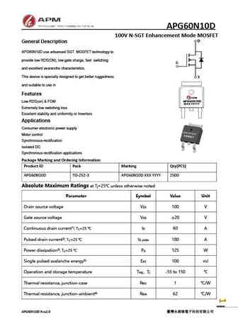
APG60N10D 100V N-SGT Enhancement Mode MOSFET General Description APG60N10D use advanced SGT MOSFET technology to provide low RDS(ON), low gate charge, fast switching and excellent avalanche characteristics. This device is specially designed to get better ruggedness and suitable to use in Features Low RDS(on) & FOM Extremely low switching loss Excellent stability and unifo
Другие MOSFET... 2SK2020-01MR , 2SK2645 , 2SK2850 , 40N10 , 50N15 , 60N05 , 60N05-16 , 60N06-18 , IRFP260 , 6N70A , 75N06 , 75N10 , 75NF75 , BUK436-100A , BUK436-100B , BUK436-200A , BUK436-200B .
History: 2SJ378
History: 2SJ378
🌐 : EN ES РУ

Список транзисторов
Обновления
MOSFET: ASD80R750E | ASD70R950E | ASD70R600E | ASD70R380E | ASD65R850E | ASD65R550E | ASD65R350E | ASD65R300E | ASD65R280E | ASD65R270E | ASD60R330E | ASD60R280E | ASB80R750E | ASB70R380E | ASB65R300E | ASB65R220E
Popular searches
irfp260 | ksc2383 | 2n3773 | b772 transistor | 50n06 | mje350 | 2n3866 | irf 3205