IPP032N06N3. Аналоги и основные параметры
Наименование производителя: IPP032N06N3
Тип транзистора: MOSFET
Полярность: N
Предельные значения
Pd ⓘ
- Максимальная рассеиваемая мощность: 188 W
|Vds|ⓘ - Максимально допустимое напряжение сток-исток: 60 V
|Vgs|ⓘ - Максимально допустимое напряжение затвор-исток: 20 V
|Id| ⓘ - Максимально допустимый постоянный ток стока: 120 A
Tj ⓘ - Максимальная температура канала: 175 °C
Электрические характеристики
tr ⓘ -
Время нарастания: 120 ns
Cossⓘ - Выходная емкость: 2200 pf
RDSonⓘ - Сопротивление сток-исток открытого транзистора: 0.0032 Ohm
Тип корпуса: TO220
Аналог (замена) для IPP032N06N3
- подборⓘ MOSFET транзистора по параметрам
IPP032N06N3 даташит
..1. Size:246K inchange semiconductor
ipp032n06n3.pdf 
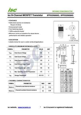
INCHANGE Semiconductor isc N-Channel MOSFET Transistor IPP032N06N3 IIPP032N06N3 FEATURES Static drain-source on-resistance RDS(on) 2.9m Enhancement mode Fast Switching Speed 100% avalanche tested Minimum Lot-to-Lot variations for robust device performance and reliable operation DESCRITION reliable device for use in a wide variety of applications ABSOLUTE M
0.1. Size:483K infineon
ipb029n06n3g ipi032n06n3g ipp032n06n3g.pdf 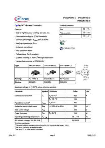
Type IPB029N06N3 G IPI032N06N3 G IPP032N06N3 G OptiMOS 3 Power-Transistor Product Summary V 60 V Features DS R 2.9 m Ideal for high frequency switching and sync. rec. DS(on),max (SMD) I 120 A Optimized technology for DC/DC converters D Excellent gate charge x R product (FOM) DS(on) Very low on-resistance RDS(on) N-channel, normal level 100% avalanche t
0.2. Size:2470K cn vbsemi
ipp032n06n3g.pdf 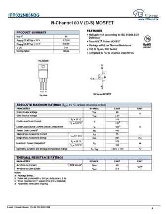
IPP032N06N3G www.VBsemi.tw N-Channel 60 V (D-S) MOSFET FEATURES PRODUCT SUMMARY Halogen-free According to IEC 61249-2-21 VDS (V) 60 Definition RDS(on) ( ) at VGS = 10 V 0.0035 TrenchFET Power MOSFET RDS(on) ( ) at VGS = 4.5 V 0.0090 Package with Low Thermal Resistance ID (A) 210 100 % Rg and UIS Tested Configuration Single Compliant to RoHS Directive 200
9.1. Size:460K 1
ipi034ne7n3g ipp034ne7n3g.pdf 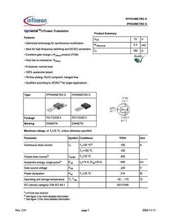
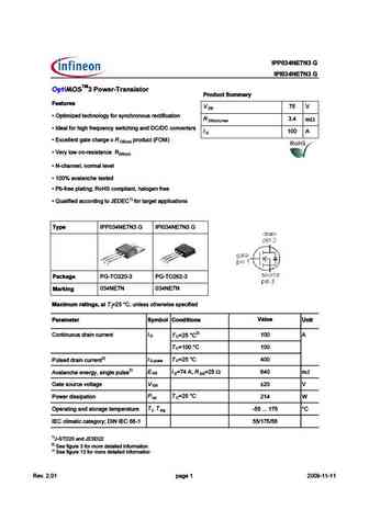
IPP034NE7N3 G IPI034NE7N3 G OptiMOSTM3 Power-Transistor Product Summary Features V 75 V DS Optimized technology for synchronous rectification R 3.4 m DS(on),max Ideal for high frequency switching and DC/DC converters I 100 A D Excellent gate charge x R product (FOM) DS(on) Very low on-resistance RDS(on) N-channel, normal level 100% avalanche tested
9.2. Size:475K infineon
ipb034n06l3g ipi037n06l3g ipp037n06l3g.pdf 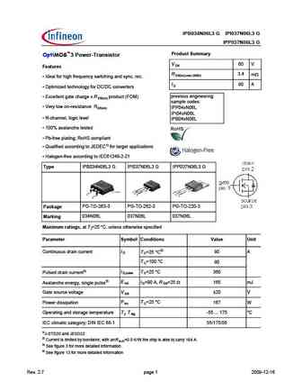
Type IPB034N06L3 G IPI037N06L3 G IPP037N06L3 G Product Summary OptiMOS 3 Power-Transistor V 60 V DS Features R 3.4 m DS(on),max (SMD) Ideal for high frequency switching and sync. rec. I 90 A D Optimized technology for DC/DC converters previous engineering Excellent gate charge x R product (FOM) DS(on) sample codes Very low on-resistance RDS(on) IPP04xN06
9.3. Size:264K infineon
ipp039n04lg ipb039n04lg.pdf 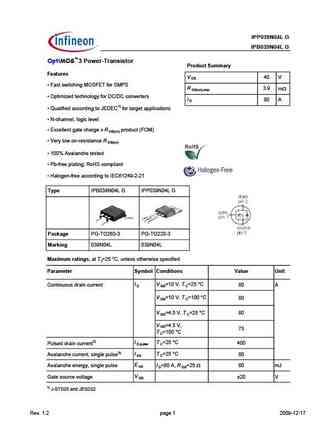
Type IPP039N04L G IPB039N04L G OptiMOS 3 Power-Transistor Product Summary Features V 40 V DS Fast switching MOSFET for SMPS R 3.9 m DS(on),max Optimized technology for DC/DC converters I 80 A D Qualified according to JEDEC1) for target applications N-channel, logic level Excellent gate charge x R product (FOM) DS(on) Very low on-resistance R DS(on
9.4. Size:1018K infineon
ipp037n08n3ge8181 ipp037n08n3g ipi037n08n3g ipb035n08n3g.pdf 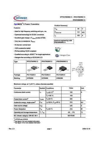
IPP037N08N3 G IPI037N08N3 G IPB035N08N3 G 3 Power-Transistor Product Summary Features V D Q #4513I CG9D389>7 1>4 CI>3 B53 R m D n) m x Q ( @D9=9J54 D538>?F5BD5BC I 1 D Q H3579>55B9>7 3?45 Q .5BI B5C9CD1>35 + D n) #) ' ' ! Q ' 381>>5?B=1
9.5. Size:344K infineon
ipb039n04l-g ipp039n04l-g.pdf 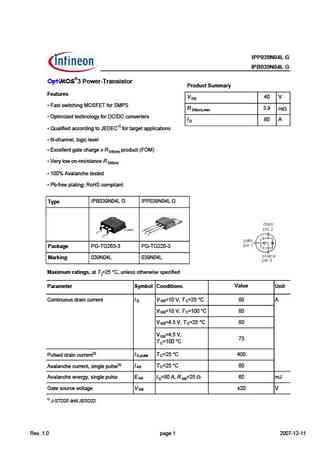
Type IPP039N04L G IPB039N04L G OptiMOS 3 Power-Transistor Product Summary Features V 40 V DS Fast switching MOSFET for SMPS R 3.9 m DS(on),max Optimized technology for DC/DC converters I 80 A D Qualified according to JEDEC1) for target applications N-channel, logic level Excellent gate charge x R product (FOM) DS(on) Very low on-resistance R DS(on
9.6. Size:1820K infineon
ipp030n10n5.pdf 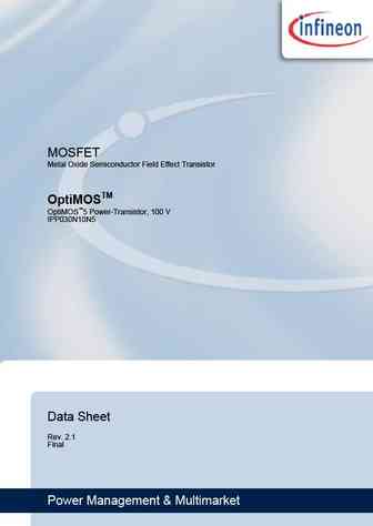
MOSFET Metal Oxide Semiconductor Field Effect Transistor OptiMOSTM OptiMOS 5 Power-Transistor, 100 V IPP030N10N5 Data Sheet Rev. 2.1 Final Power Management & Multimarket OptiMOS 5 Power-Transistor, 100 V IPP030N10N5 TO-220-3 1 Description tab Features Ideal for high frequency switching and sync. rec. Excellent gate charge x R product (FOM) DS(on) Very low on-re
9.7. Size:1541K infineon
ipp039n10n5.pdf 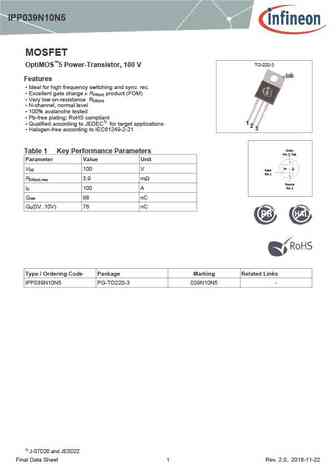
IPP039N10N5 MOSFET TO-220-3 OptiMOS 5 Power-Transistor, 100 V tab Features Ideal for high frequency switching and sync. rec. Excellent gate charge x R product (FOM) DS(on) Very low on-resistance R DS(on) N-channel, normal level 100% avalanche tested Pb-free plating; RoHS compliant Qualified according to JEDEC1) for target applications Halogen-free
9.8. Size:575K infineon
ipp030n10n3g.pdf 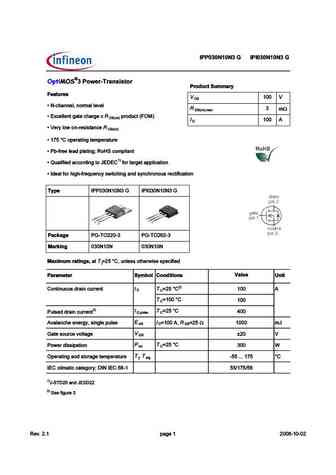
$$ " " $ " " $;B1= '=- >5>?;= $=;0@/? &@99-=D Features 1 D Q ' 381>>5?B=1
9.9. Size:726K infineon
ipp034n03l .pdf 
Type IPP034N03L G IPB034N03L G 3 Power-Transistor Product Summary Features V 30 V DS Fast switching MOSFET for SMPS R 3.4 mW DS(on),max Optimized technology for DC/DC converters I 80 A D Qualified according to JEDEC1) for target applications N-channel, logic level Excellent gate charge x R product (FOM) DS(on) Very low on-resistance R DS(on)
9.10. Size:536K infineon
ipi030n10n3g ipp030n10n3g ipp030n10n3g ipi030n10n3g.pdf 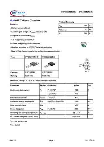
IPP030N10N3 G IPI030N10N3 G OptiMOS 3 Power-Transistor Product Summary Features VDS 100 V N-channel, normal level RDS(on),max 3 mW Excellent gate charge x R product (FOM) DS(on) ID 100 A Very low on-resistance R DS(on) 175 C operating temperature Pb-free lead plating; RoHS compliant Qualified according to JEDEC1) for target application Ideal for h
9.11. Size:725K infineon
ipp034n03lg ipb034n03lg.pdf 
Type IPP034N03L G IPB034N03L G 3 Power-Transistor Product Summary Features V 30 V DS Fast switching MOSFET for SMPS R 3.4 mW DS(on),max Optimized technology for DC/DC converters I 80 A D Qualified according to JEDEC1) for target applications N-channel, logic level Excellent gate charge x R product (FOM) DS(on) Very low on-resistance R DS(on)
9.13. Size:1806K infineon
ipp034n08n5.pdf 
MOSFET Metal Oxide Semiconductor Field Effect Transistor OptiMOSTM OptiMOS 5 Power-Transistor, 80 V IPP034N08N5 Data Sheet Rev. 2.0 Final Power Management & Multimarket OptiMOS 5 Power-Transistor, 80 V IPP034N08N5 TO-220-3 1 Description tab Features Ideal for high frequency switching and sync. rec. Excellent gate charge x R product (FOM) DS(on) Very low on-resis
9.14. Size:494K infineon
ipp037n08n3g ipi037n08n3g ipb035n08n3g.pdf 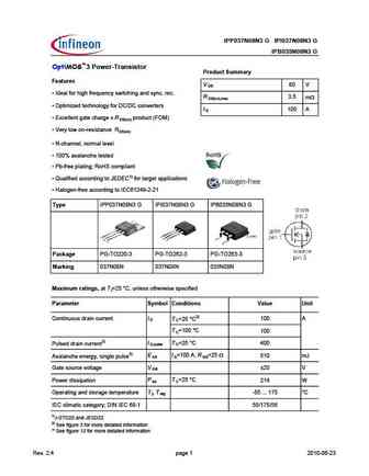
IPP037N08N3 G IPI037N08N3 G IPB035N08N3 G OptiMOS 3 Power-Transistor Product Summary Features V 80 V DS Ideal for high frequency switching and sync. rec. R 3.5 m DS(on),max Optimized technology for DC/DC converters I 100 A D Excellent gate charge x R product (FOM) DS(on) Very low on-resistance RDS(on) N-channel, normal level 100% avalanche tested
9.15. Size:723K infineon
ipb034n03l ipp034n03l.pdf 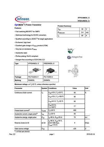
Type IPP034N03L G IPB034N03L G 3 Power-Transistor Product Summary Features V 30 V DS Fast switching MOSFET for SMPS R 3.4 mW DS(on),max Optimized technology for DC/DC converters I 80 A D Qualified according to JEDEC1) for target applications N-channel, logic level Excellent gate charge x R product (FOM) DS(on) Very low on-resistance R DS(on)
9.16. Size:246K inchange semiconductor
ipp034n03l.pdf 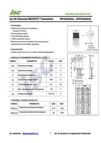
INCHANGE Semiconductor isc N-Channel MOSFET Transistor IPP034N03L IIPP034N03L FEATURES Static drain-source on-resistance RDS(on) 3.4m Enhancement mode Fast Switching Speed 100% avalanche tested Minimum Lot-to-Lot variations for robust device performance and reliable operation DESCRITION reliable device for use in a wide variety of applications ABSOLUTE
9.17. Size:246K inchange semiconductor
ipp037n06l3.pdf 
INCHANGE Semiconductor isc N-Channel MOSFET Transistor IPP037N06L3 IIPP037N06L3 FEATURES Static drain-source on-resistance RDS(on) 3.4m Enhancement mode Fast Switching Speed 100% avalanche tested Minimum Lot-to-Lot variations for robust device performance and reliable operation DESCRITION reliable device for use in a wide variety of applications ABSOLUTE M
9.18. Size:245K inchange semiconductor
ipp030n10n5.pdf 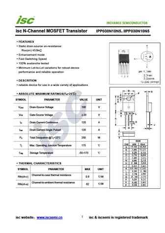
INCHANGE Semiconductor isc N-Channel MOSFET Transistor IPP030N10N5 IIPP030N10N5 FEATURES Static drain-source on-resistance RDS(on) 3.0m Enhancement mode Fast Switching Speed 100% avalanche tested Minimum Lot-to-Lot variations for robust device performance and reliable operation DESCRITION reliable device for use in a wide variety of applications ABSOLUTE
9.19. Size:246K inchange semiconductor
ipp039n10n5.pdf 
INCHANGE Semiconductor isc N-Channel MOSFET Transistor IPP039N10N5 IIPP039N10N5 FEATURES Static drain-source on-resistance RDS(on) 3.9m Enhancement mode Fast Switching Speed 100% avalanche tested Minimum Lot-to-Lot variations for robust device performance and reliable operation DESCRITION reliable device for use in a wide variety of applications ABSOLUTE
9.20. Size:245K inchange semiconductor
ipp030n10n3.pdf 
INCHANGE Semiconductor isc N-Channel MOSFET Transistor IPP030N10N3 IIPP030N10N3 FEATURES Static drain-source on-resistance RDS(on) 3m Enhancement mode Fast Switching Speed 100% avalanche tested Minimum Lot-to-Lot variations for robust device performance and reliable operation DESCRITION reliable device for use in a wide variety of applications ABSOLUTE M
9.21. Size:246K inchange semiconductor
ipp037n08n3.pdf 
INCHANGE Semiconductor isc N-Channel MOSFET Transistor IPP037N08N3 IIPP037N08N3 FEATURES Static drain-source on-resistance RDS(on) 3.75m Enhancement mode Fast Switching Speed 100% avalanche tested Minimum Lot-to-Lot variations for robust device performance and reliable operation DESCRITION reliable device for use in a wide variety of applications ABSOLUT
9.22. Size:246K inchange semiconductor
ipp034n08n5.pdf 
INCHANGE Semiconductor isc N-Channel MOSFET Transistor IPP034N08N5 IIPP034N08N5 FEATURES Static drain-source on-resistance RDS(on) 3.4m Enhancement mode Fast Switching Speed 100% avalanche tested Minimum Lot-to-Lot variations for robust device performance and reliable operation DESCRITION reliable device for use in a wide variety of applications ABSOLUTE
9.23. Size:246K inchange semiconductor
ipp039n04l.pdf 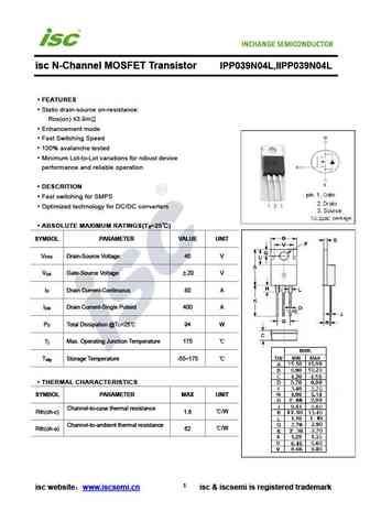
isc N-Channel MOSFET Transistor IPP039N04L,IIPP039N04L FEATURES Static drain-source on-resistance RDS(on) 3.9m Enhancement mode Fast Switching Speed 100% avalanche tested Minimum Lot-to-Lot variations for robust device performance and reliable operation DESCRITION Fast switching for SMPS Optimized technology for DC/DC converters ABSOLUTE MAXIMUM RATINGS(T
Другие MOSFET... FMV09N70E
, FRK250
, FRM230
, FRM240
, IPP015N04N
, IPP023NE7N3
, IPP024N06N3
, IPP030N10N3
, 20N50
, IPP037N06L3
, IPP037N08N3
, IPP039N10N5
, IPP040N06N3
, IPP048N04N
, IPP052NE7N3
, IPP062NE7N3
, IPP065N03L
.