40N06. Аналоги и основные параметры
Наименование производителя: 40N06
Тип транзистора: MOSFET
Полярность: N
Предельные значения
Pd ⓘ - Максимальная рассеиваемая мощность: 120 W
|Vds|ⓘ - Максимально допустимое напряжение сток-исток: 60 V
|Vgs|ⓘ - Максимально допустимое напряжение затвор-исток: 30 V
|Id| ⓘ - Максимально допустимый постоянный ток стока: 40 A
Tj ⓘ - Максимальная температура канала: 150 °C
Электрические характеристики
tr ⓘ - Время нарастания: 330 ns
Cossⓘ - Выходная емкость: 2500 pf
RDSonⓘ - Сопротивление сток-исток открытого транзистора: 0.035 Ohm
Тип корпуса: TO220
Аналог (замена) для 40N06
- подборⓘ MOSFET транзистора по параметрам
40N06 даташит
40n06.pdf
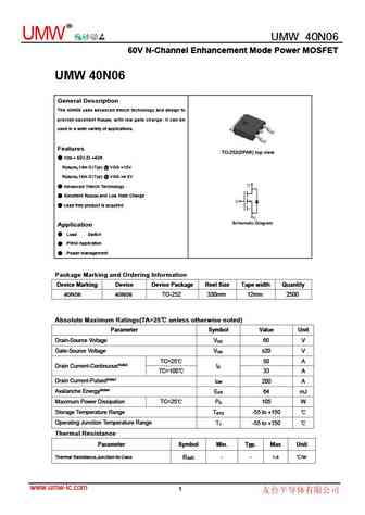
R UMW UMW 40N06 60V N-Channel Enhancement Mode Power MOSFET UMW 40N06 General Description The 40N06 uses advanced trench technology and design to provide excellent RDS(ON) with low gate charge. It can be used in a wide variety of applications. Features VDS = 60V,ID =40A RDS(ON),14m (Typ) @ VGS =10V RDS(ON),16m (Typ) @ VGS =4.5V Advanced Trench Technology Excellent RDS(ON) and L
40n06.pdf
40N06 60V N-Channel Enhancement Mode Power MOSFET 40N06 General Description The 40N06 uses advanced trench technology and design to provide excellent RDS(ON) with low gate charge. It can be used in a wide variety of applications. Features VDS = 60V,ID =40A RDS(ON),14m (Typ) @ VGS =10V RDS(ON),16m (Typ) @ VGS =4.5V Advanced Trench Technology Excellent RDS(ON) and Low Gate Charge
40n06.pdf
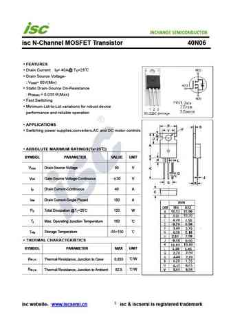
isc N-Channel MOSFET Transistor 40N06 FEATURES Drain Current I = 40A@ T =25 D C Drain Source Voltage- V = 60V(Min) DSS Static Drain-Source On-Resistance R = 0.035 (Max) DS(on) Fast Switching Minimum Lot-to-Lot variations for robust device performance and reliable operation APPLICATIONS Switching power supplies,converters,AC and DC motor controls ABSOLUTE
fdi040n06.pdf
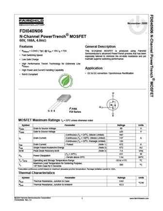
November 2009 FDI040N06 N-Channel PowerTrench MOSFET 60V, 168A, 4.0m Features General Description RDS(on) = 3.2m ( Typ.) @ VGS = 10V, ID = 75A This N-Channel MOSFET is produced using Fairchild Semiconductor s advanced PowerTrench process that has been Fast Switching Speed especially tailored to minimize the on-state resistance and yet maintain superior switching p
fdp040n06.pdf
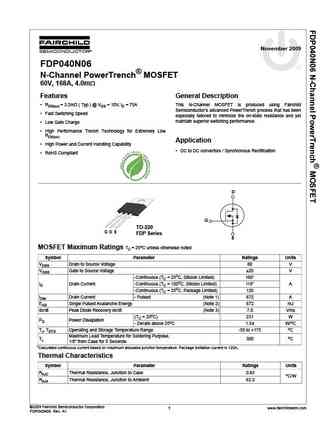
November 2009 FDP040N06 N-Channel PowerTrench MOSFET 60V, 168A, 4.0m Features General Description RDS(on) = 3.2m ( Typ.) @ VGS = 10V, ID = 75A This N-Channel MOSFET is produced using Fairchild Semiconductor s advanced PowerTrench process that has been Fast Switching Speed especially tailored to minimize the on-state resistance and yet maintain superior switching p
sup40n06-25l sub40n06-25l.pdf
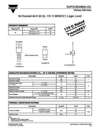
SUP/SUB40N06-25L Vishay Siliconix N-Channel 60-V (D-S), 175_C MOSFET, Logic Level PRODUCT SUMMARY V(BR)DSS (V) rDS(on) (W) ID (A) 0.022 @ VGS = 10 V 40 60 60 0.025 @ VGS = 4.5 V 40 TO-220AB D TO-263 G DRAIN connected to TAB G D S Top View G D S SUB40N06-25L S Top View N-Channel MOSFET SUP40N06-25L ABSOLUTE MAXIMUM RATINGS (TC = 25_C UNLESS OTHERWISE NOTED) Parameter Symbol
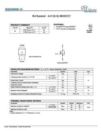
sqd40n06-14l.pdf
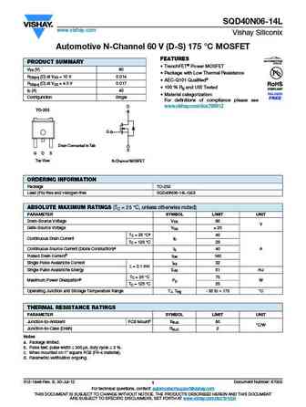
SQD40N06-14L www.vishay.com Vishay Siliconix Automotive N-Channel 60 V (D-S) 175 C MOSFET FEATURES PRODUCT SUMMARY TrenchFET Power MOSFET VDS (V) 60 Package with Low Thermal Resistance RDS(on) ( ) at VGS = 10 V 0.014 AEC-Q101 Qualifiedd RDS(on) ( ) at VGS = 4.5 V 0.017 100 % Rg and UIS Tested ID (A) 40 Material categorization Configuration Single
sud40n06-25l.pdf
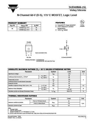
SUD40N06-25L Vishay Siliconix N-Channel 60-V (D-S), 175_C MOSFET, Logic Level FEATURES PRODUCT SUMMARY Pb-free D TrenchFETr Power MOSFET VDS (V) rDS(on) (W) ID (A)a Available D 175_C Maximum Junction 0.022 @ VGS = 10 V 30 Temperature 60 60 0.025 @ VGS = 4.5 V 30 D 100% Rg Tested D TO-252 G Drain Connected to Tab S G D S Top View N-Channel MOSFET Ordering Information SUD4
ipb037n06n3g ipi040n06n3g ipp040n06n3g.pdf
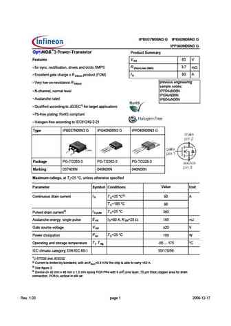
Type IPB037N06N3 G IPI040N06N3 G IPP040N06N3 G OptiMOS 3 Power-Transistor Product Summary Features V 60 V DS R 3.7 for sync. rectification, drives and dc/dc SMPS m DS(on),max (SMD) I 90 A Excellent gate charge x R product (FOM) D DS(on) previous engineering Very low on-resistance R DS(on) sample codes N-channel, normal level IPP04xN06N IPI04xN06N Ava
ipa040n06nm5s.pdf
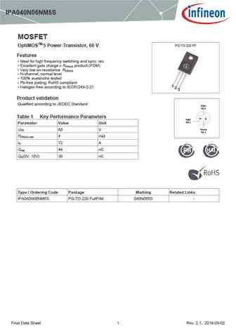
IPA040N06NM5S MOSFET PG-TO 220 FP OptiMOSTM 5 Power-Transistor, 60 V Features Ideal for high frequency switching and sync. rec. Excellent gate charge x R product (FOM) DS(on) Very low on-resistance R DS(on) N-channel, normal level 100% avalanche tested Pb-free plating; RoHS compliant Halogen-free according to IEC61249-2-21 Product validation Qualified
bsz040n06ls5.pdf
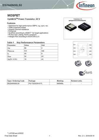
BSZ040N06LS5 MOSFET TSDSON-8 FL OptiMOSTM Power-Transistor, 60 V (enlarged source interconnection) Features Optimized for high performance SMPS, e.g. sync. rec. 100% avalanche tested Superior thermal resistance N-channel Qualified according to JEDEC1) for target applications Pb-free lead plating; RoHS compliant Halogen-free according to IEC61249-2-21 Tab
ipp040n06n3g.pdf
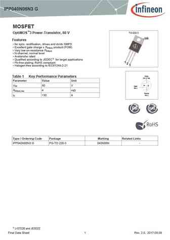
IPP040N06N3 G MOSFET TO-220-3 OptiMOS 3 Power-Transistor, 60 V tab Features for sync. rectification, drives and dc/dc SMPS Excellent gate charge x R product (FOM) DS(on) Very low on-resistance R DS(on) N-channel, normal level Avalanche rated Qualified according to JEDEC1) for target applications Pb-free plating; RoHS compliant Halogen-free accordi
ipa040n06n.pdf
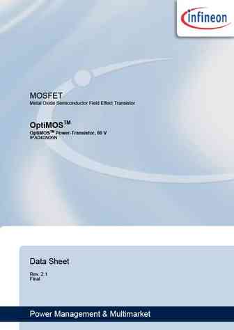
MOSFET Metal Oxide Semiconductor Field Effect Transistor OptiMOSTM OptiMOSTM Power-Transistor, 60 V IPA040N06N Data Sheet Rev. 2.1 Final Power Management & Multimarket OptiMOSTM Power-Transistor, 60 V IPA040N06N TO-220-FP 1 Description Features Optimized for high performance SMPS, e.g. sync. rec. 100% avalanche tested Superior thermal resistance N-channel
ipp040n06n.pdf
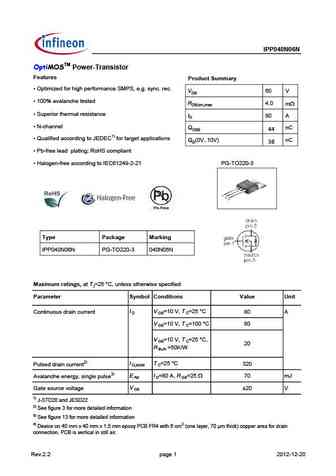
Type IPP040N06N OptiMOSTM Power-Transistor Features Product Summary Optimized for high performance SMPS, e.g. sync. rec. VDS 60 V 100% avalanche tested RDS(on),max 4.0 mW Superior thermal resistance ID 80 A N-channel QOSS nC 44 Qualified according to JEDEC1) for target applications QG(0V..10V) nC 38 Pb-free lead plating; RoHS compliant Hal
ipd640n06lg ipd640n06l g.pdf
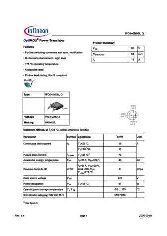
% # ! % (>.;?6?@ %>E Features D P ?A 61BC BF9C389>7 3?>E5AC5AB 1>4 BH>3 A53C96931C9?> 4 mW D n) m x P ( 381>>581>35=5>C
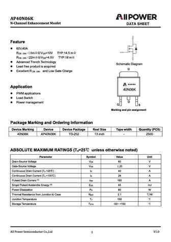
am40n06-28d.pdf
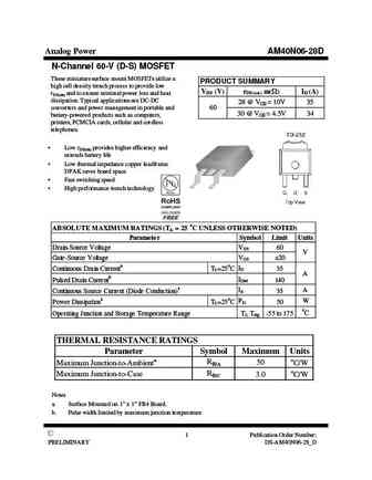
Analog Power AM40N06-28D N-Channel 60-V (D-S) MOSFET These miniature surface mount MOSFETs utilize a PRODUCT SUMMARY high cell density trench process to provide low VDS (V) rDS(on) m( ) ID (A) rDS(on) and to ensure minimal power loss and heat dissipation. Typical applications are DC-DC 28 @ VGS = 10V 35 converters and power management in portable and 60 30 @ VGS = 4.5V 34 batte
mtb40n06e3.pdf
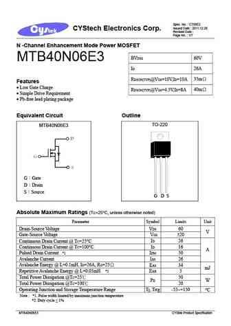
Spec. No. C708E3 Issued Date 2011.12.26 CYStech Electronics Corp. Revised Date Page No. 1/7 N -Channel Enhancement Mode Power MOSFET BVDSS 60V MTB40N06E3 ID 26A 35m RDSON(TYP)@VGS=10V,ID=10A Features Low Gate Charge 40m RDSON(TYP)@VGS=4.5V,ID=8A Simple Drive Requirement Pb-free lead plating package Equivalent Circuit Outline TO-220 MTB
cs40n06.pdf
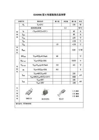
CS40N06 N PD TC=25 150 W 1.2 W/ ID VGS=10V,TC=25 40 A IDM 60 A VGS 20 V Tjm +150 Tstg -55 +150 RthJC 0.83 /W BVDSS VGS=0V,ID=0.25mA 60 V RDS on VGS=10V,ID=20A 0.055 VGS th VDS=VGS,ID=0.25mA 2.0 4.0 V
dh240n06l dh240n06lf dh240n06li dh240n06le dh240n06lb dh240n06ld.pdf
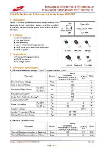
DH240N06L/DH240N06LF/DH240N06LI/ DH240N06LE/DH240N06LB/DH240N06LD 33A 60V N-channel Enhancement Mode Power MOSFET 1 Description These N-channel enhancement mode power mosfets used 2 D V = 60V DSS advanced trench technology design, provided excellent Rdson and low gate charge. Which accords with the RoHS G R = 24m DS(on) (TYP) standard. 1 3 S I = 33A D 2 Features Low on
ms40n06.pdf
MS40N06 60V N-Channel MOSFET GENERAL DESCRIPTION The MS40N06 is the highest performance trench N-ch MOSFETs with extreme high cell density , which provide excellent RDSON and gate charge for most of the synchronous buck converter applications . The QM6006M6 meet the RoHS and Green Product requirement , 100% EAS guaranteed with full function reliability approved. FEATURES Ad
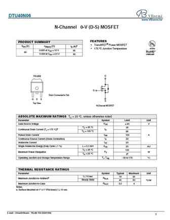
dtu40n06.pdf
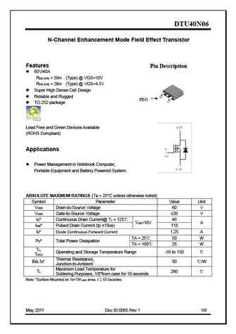
DTU40N06 N-Channel Enhancement Mode Field Effect Transistor Features Pin Description 60V/40A RDS (ON) = 20m (Type) @ VGS=10V RDS (ON) = 28m (Type) @ VGS=4.5V Super High Dense Cell Design Reliable and Rugged PIN1 TO-252 package Lead Free and Green Devices Available (ROHS Compliant) Applications Power Management in Notebook Computer, Portable Equipment and Ba
swha40n06v.pdf
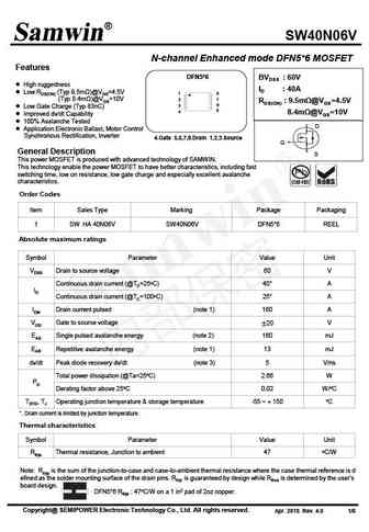
SW40N06V N-channel Enhanced mode DFN5*6 MOSFET Features DFN5*6 BVDSS 60V High ruggedness ID 40A Low RDS(ON) (Typ 9.5m )@VGS=4.5V 1 8 (Typ 8.4m )@VGS=10V 2 7 RDS(ON) 9.5m @VGS=4.5V 6 3 Low Gate Charge (Typ 83nC) 5 4 8.4m @VGS=10V Improved dv/dt Capability 100% Avalanche Tested D Application Electronic Ballast, Moto
sre40n065fsu2dg.pdf

Datasheet 40A 650V Trench Field stop IGBT with FRD SRE40N065FSU2DG General Description Symbol The SRE40N065FSU2DG is a Field Stop Trench IGBT with anti-parallel diode, which offers ultra- low switching losses, high energy efficiency for switching applications such as PFC, Power Supply, Inverter, etc. The SRE40N065FSU2DG is available in TO-263 and TO-247 packages. Figure 1 Sy
sre40n065fsur.pdf
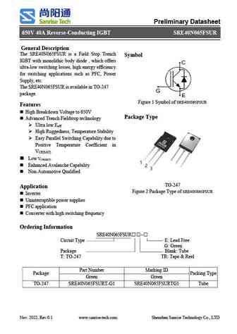
Preliminary Datasheet 650V 40A Reverse-Conducting IGBT SRE40N065FSUR General Description The SRE40N065FSUR is a Field Stop Trench Symbol IGBT with monolithic body diode , which offers ultra-low switching losses, high energy efficiency for switching applications such as PFC, Power Supply, etc. The SRE40N065FSUR is available in TO-247 package. Figure 1 Symbol of SRE40N065F
sre40n065fsudg.pdf
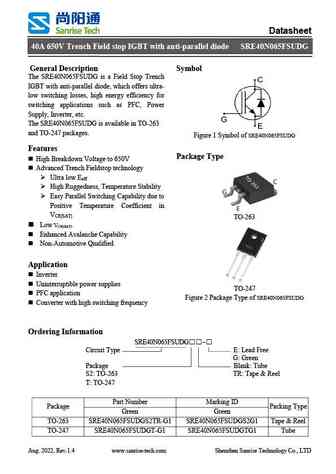
Datasheet 40A 650V Trench Field stop IGBT with anti-parallel diode SRE40N065FSUDG General Description Symbol The SRE40N065FSUDG is a Field Stop Trench IGBT with anti-parallel diode, which offers ultra- low switching losses, high energy efficiency for switching applications such as PFC, Power Supply, Inverter, etc. The SRE40N065FSUDG is available in TO-263 and TO-247 packages.
sre40n065fsudf.pdf
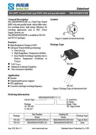
Datasheet 40A 650V Trench Field stop IGBT with anti-parallel diode SRE40N065FSUDF General Description Symbol The SRE40N065FSUDF is a Field Stop Trench IGBT with anti-parallel diode, which offers ultra- low switching losses, high energy efficiency for switching applications such as PFC, Power Supply, Inverter, etc. The SRE40N065FSUDF is available in TO-263 and TO-247 packages.
sre40n065fsu2df.pdf
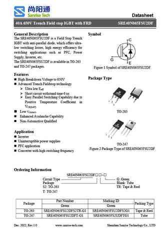
Datasheet 40A 650V Trench Field stop IGBT with FRD SRE40N065FSU2DF General Description Symbol The SRE40N065FSU2DF is a Field Stop Trench IGBT with anti-parallel diode, which offers ultra- low switching losses, high energy efficiency for switching applications such as PFC, Power Supply, Inverter, etc. The SRE40N065FSU2DF is available in TO-263 and TO-247 packages. Figure 1 Sy
hrp140n06k.pdf
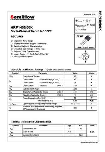
December 2014 BVDSS = 60 V RDS(on) typ = 11.5m HRP140N06K ID = 40 A 60V N-Channel Trench MOSFET TO-220 FEATURES Originative New Design Superior Avalanche Rugged Technology 1 2 3 Excellent Switching Characteristics 1.Gate 2. Drain 3. Source Unrivalled Gate Charge 40 nC (Typ.) Extended Safe Operating Area Lower RDS(ON) 11.5 m (Typ
hrf140n06k.pdf
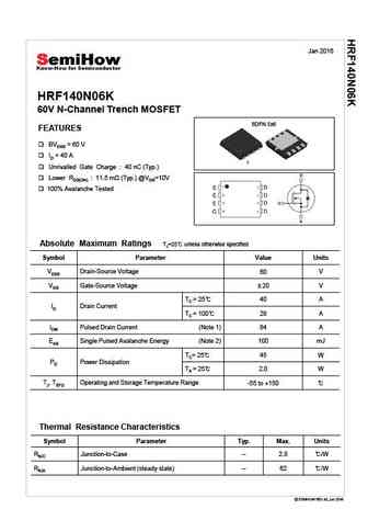
Jan 2016 HRF140N06K 60V N-Channel Trench MOSFET 8DFN 5x6 FEATURES BVDSS = 60 V ID = 40 A 1 Unrivalled Gate Charge 40 nC (Typ.) Lower RDS(ON) 11.5 (Typ.) @VGS=10V 100% Avalanche Tested Absolute Maximum Ratings TJ=25 unless otherwise specified Symbol Parameter Value Units VDSS Drain-Source Voltage 60 V VGS Gate-Source Voltage 20 V TC = 25 40 A ID Drain Current TC
hrs140n06k.pdf
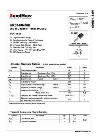
December 2014 BVDSS = 60 V RDS(on) typ HRS140N06K ID = 40 A 60V N-Channel Trench MOSFET TO-220F FEATURES Originative New Design Superior Avalanche Rugged Technology 1 2 3 Excellent Switching Characteristics 1.Gate 2. Drain 3. Source Unrivalled Gate Charge 40 nC (Typ.) Extended Safe Operating Area Lower RDS(ON) 11.5 (Typ.) @VGS=10V 100% Avalanche Te
tx40n06b.pdf
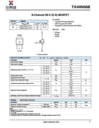
TX40N06B N-Channel 60-V (D-S) MOSFET FE ATURES PRODUCT SUMMARY TrenchFET Power MOSFET VDS (V) RDS(on) ( ) ID (A)a, e Qg (Typ) 100 % Rg and UIS Tested Compliant to RoHS Directive 2011/65/EU 0.025 at VGS = 10 V 35 60 81 nC 0.030 at VGS = 4.5 V 32 APPLICAT IONS D OR-ing Server TO-252 DC/DC G G D S Top View S N-Channel MOSFET ABSOLUTE MAXIMUM RAT
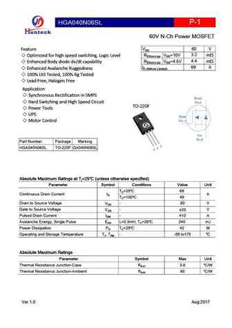
hga040n06s.pdf
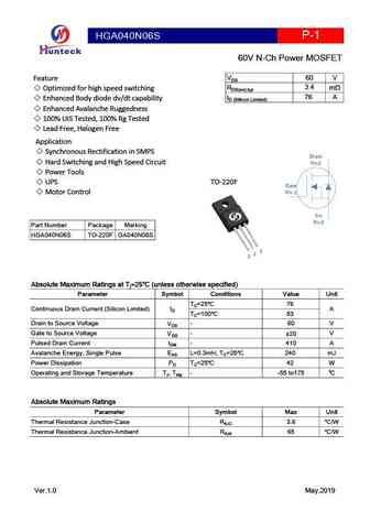
HGA040N06S P-1 60V N-Ch Power MOSFET 60 V VDS Feature 3.4 RDS(on),typ m Optimized for high speed switching 76 A ID (Sillicon Limited) Enhanced Body diode dv/dt capability Enhanced Avalanche Ruggedness 100% UIS Tested, 100% Rg Tested Lead Free, Halogen Free Application Synchronous Rectification in SMPS Drain Hard Switching and High Speed Circuit P
hgb040n06sl hgp040n06sl.pdf
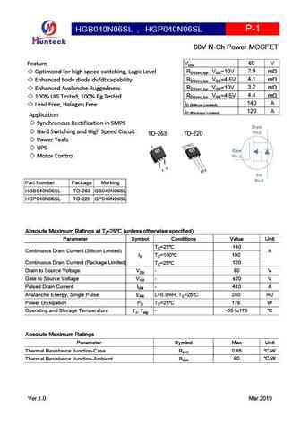
HGB040N06SL HGP040N06SL P-1 , 60V N-Ch Power MOSFET 60 V VDS Feature 2.9 RDS(on),typ VGS=10V m Optimized for high speed switching, Logic Level 4.1 RDS(on),typ VGS=4.5V m Enhanced Body diode dv/dt capability 3.2 RDS(on),typ VGS=10V m Enhanced Avalanche Ruggedness 4.4 RDS(on),typ VGS=4.5V m 100% UIS Tested, 100% Rg Tested 140 A ID (Sillicon Limited)
hgd040n06sl hgi040n06sl.pdf
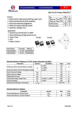
HGD040N06SL HGI040N06SL P-1 , 60V N-Ch Power MOSFET 60 V VDS Feature 3.3 RDS(on),typ VGS=10V m Optimized for high speed switching, Logic Level 4 RDS(on),typ VGS=4.5V m Enhanced Body diode dv/dt capability 132 A ID (Sillicon Limited) Enhanced Avalanche Ruggedness 70 A ID (Package Limited) 100% UIS Tested, 100% Rg Tested Lead Free, Halogen Free Applica
hgd040n06s.pdf
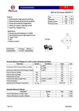
P-1 HGD040N06S 60V N-Ch Power MOSFET 60 V VDS Feature 3.4 RDS(on),typ mW Optimized for high speed switching 144 A ID (Sillicon Limited) Enhanced Body diode dv/dt capability 70 A ID (Package Limited) Enhanced Avalanche Ruggedness 100% UIS Tested, 100% Rg Tested Lead Free, Halogen Free Application Synchronous Rectification in SMPS Drain Hard Switchi
hga040n06sl.pdf
HGA040N06SL P-1 60V N-Ch Power MOSFET 60 V VDS Feature 3.2 RDS(on),typ VGS=10V m Optimized for high speed switching, Logic Level 4.4 RDS(on),typ VGS=4.5V m Enhanced Body diode dv/dt capability 69 A ID (Sillicon Limited) Enhanced Avalanche Ruggedness 100% UIS Tested, 100% Rg Tested Lead Free, Halogen Free Application Synchronous Rectification in SMP
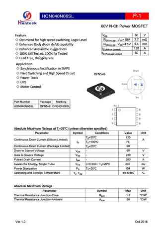
hgn040n06s.pdf
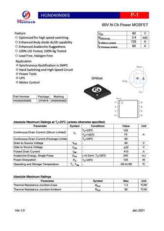
HGN040N06S P-1 60V N-Ch Power MOSFET 60 V Feature VDS 3.4 Optimized for high speed switching RDS(on),typ mW 125 A ID (Sillicon Limited) Enhanced Body diode dv/dt capability 60 A ID (Package Limited) Enhanced Avalanche Ruggedness 100% UIS Tested, 100% Rg Tested Lead Free, Halogen Free Application Synchronous Rectification in SMPS Drain Hard Switching
hgb040n06s hgp040n06s.pdf
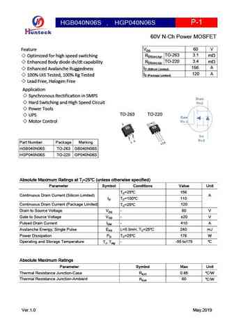
HGB040N06S HGP040N06S P-1 , 60V N-Ch Power MOSFET 60 V VDS Feature TO-263 3.1 RDS(on),typ m Optimized for high speed switching TO-220 3.4 RDS(on),typ m Enhanced Body diode dv/dt capability 156 A ID (Sillicon Limited) Enhanced Avalanche Ruggedness 120 A ID (Package Limited) 100% UIS Tested, 100% Rg Tested Lead Free, Halogen Free Application Synch
hgn040n06sl.pdf
HGN040N06SL P-1 60V N-Ch Power MOSFET 60 V VDS Feature 3.2 RDS(on),typ VGS=10V m Optimized for high speed switching, Logic Level 4.4 RDS(on),typ VGS=4.5V m Enhanced Body diode dv/dt capability 120 A ID (Sillicon Limited) Enhanced Avalanche Ruggedness 60 A ID (Package Limited) 100% UIS Tested, 100% Rg Tested Lead Free, Halogen Free Application Syn
wsc40n06.pdf
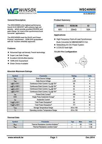
WSC40N06 N-Ch MOSFET General Description Product Summery The WSC40N06 is the highest performance BVDSS RDSON ID trench N-Ch MOSFET with extreme high cell density , which provide excellent RDSON and 60V 20m 50A gate charge for most of the synchronous buck converter applications . Applications The WSC40N06 meet the RoHS and Green High Frequency Point-of-Load Synchronous
wsf40n06.pdf
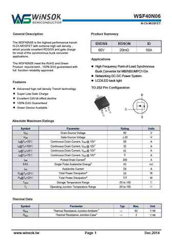
WSF40N06 N-Ch MOSFET General Description Product Summery The WSF40N06 is the highest performance trench BVDSS RDSON ID N-Ch MOSFET with extreme high cell density , which provide excellent RDSON and gate charge 60V 20m 50A for most of the synchronous buck converter applications . Applications The WSF40N06 meet the RoHS and Green High Frequency Point-of-Load Synchronous
sqd40n06-14.pdf
SQD40N06-14 www.VBsemi.tw N-Channel 6 0-V (D-S) MOSFET FEATURES PRODUCT SUMMARY TrenchFET Power MOSFET VDS (V) rDS(on) ( ) ID (A)a Available 175 C Junction Temperature 0.025 at VGS = 10 V 35 RoHS* 60 0.030 at VGS = 4.5 V 30 COMPLIANT TO-252 D G Drain Connected to Tab G D S S Top View N-Channel MOSFET ABSOLUTE MAXIMUM RATINGS TC = 25 C, unless otherwise
ipd640n06lg.pdf

IPD640N06LG www.VBsemi.tw N-Channel 6 0-V (D-S) MOSFET FEATURES PRODUCT SUMMARY TrenchFET Power MOSFET VDS (V) rDS(on) ( ) ID (A)a Available 175 C Junction Temperature 0.025 at VGS = 10 V 35 RoHS* 60 0.030 at VGS = 4.5 V 30 COMPLIANT TO-252 D G Drain Connected to Tab G D S S Top View N-Channel MOSFET ABSOLUTE MAXIMUM RATINGS TC = 25 C, unless otherwise n
dtu40n06.pdf
DTU40N06 www.VBsemi.tw N-Channel 6 0-V (D-S) MOSFET FEATURES PRODUCT SUMMARY TrenchFET Power MOSFET VDS (V) rDS(on) ( ) ID (A)a Available 175 C Junction Temperature 0.025 at VGS = 10 V 35 RoHS* 60 0.030 at VGS = 4.5 V 30 COMPLIANT TO-252 D G Drain Connected to Tab G D S S Top View N-Channel MOSFET ABSOLUTE MAXIMUM RATINGS TC = 25 C, unless otherwise no
vbzfb40n06.pdf
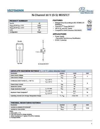
VBZFB40N06 www.VBsemi.com N-Channel 60 V (D-S) MOSFET FEATURES PRODUCT SUMMARY Halogen-free According to IEC 61249-2-21 VDS (V) 60 Definition RDS(on) ( ) at VGS = 10 V 0.032 TrenchFET Power MOSFET RDS(on) ( ) at VGS = 4.5 V 0.036 100 % Rg and UIS Tested ID (A) 25 Compliant to RoHS Directive 2002/95/EC Configuration Single APPLICATIONS Power Supply - S
vbze40n06.pdf
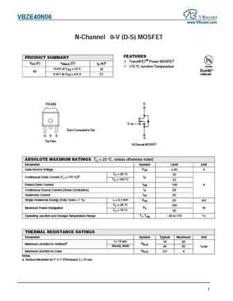
VBZE40N06 www.VBsemi.com N-Channel 6 0-V (D-S) MOSFET FEATURES PRODUCT SUMMARY TrenchFET Power MOSFET VDS (V) rDS(on) ( ) ID (A)a Available 175 C Junction Temperature 0.035 at VGS = 10 V 30 RoHS* 60 0.051 at VGS = 4.5 V 23 COMPLIANT TO-252 D G Drain Connected to Tab G D S S Top View N-Channel MOSFET ABSOLUTE MAXIMUM RATINGS TC = 25 C, unless otherwise noted
sud40n06-25l.pdf
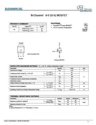
SUD40N06-25L www.VBsemi.tw N-Channel 6 0-V (D-S) MOSFET FEATURES PRODUCT SUMMARY TrenchFET Power MOSFET VDS (V) rDS(on) ( ) ID (A)a Available 175 C Junction Temperature 0.025 at VGS = 10 V 35 RoHS* 60 0.030 at VGS = 4.5 V 30 COMPLIANT TO-252 D G Drain Connected to Tab G D S S Top View N-Channel MOSFET ABSOLUTE MAXIMUM RATINGS TC = 25 C, unless otherwis
hm40n06d.pdf
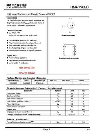
HM40N06D N-Channel Enhancement Mode Power MOSFET Description The HM40N06D uses advanced trench technology and design to provide excellent RDS(ON) with low gate charge. It can be used in a wide variety of applications. General Features VDS =60V,ID =40A RDS(ON)
mdt40n06d.pdf
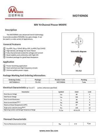
60V N-Channel Power MOSFE Description The MDT60N06 uses advanced trench technology to provide excellent RDS(ON), low gate charge. It can be used in a wide variety of applications. General Features V =60V, R
fdi040n06.pdf
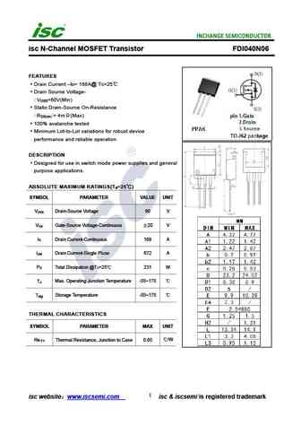
isc N-Channel MOSFET Transistor FDI040N06 FEATURES Drain Current I = 168A@ T =25 D C Drain Source Voltage- V =60V(Min) DSS Static Drain-Source On-Resistance R = 4m (Max) DS(on) 100% avalanche tested Minimum Lot-to-Lot variations for robust device performance and reliable operation DESCRIPTION Designed for use in switch mode power supplies and general purpos
ipa040n06n.pdf
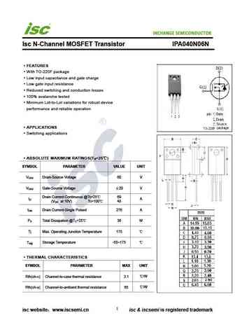
INCHANGE Semiconductor Isc N-Channel MOSFET Transistor IPA040N06N FEATURES With TO-220F package Low input capacitance and gate charge Low gate input resistance Reduced switching and conduction losses 100% avalanche tested Minimum Lot-to-Lot variations for robust device performance and reliable operation APPLICATIONS Switching applications ABSOLUTE MAXIMUM RATINGS
ipp040n06n.pdf
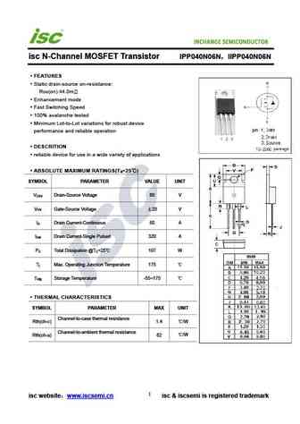
INCHANGE Semiconductor isc N-Channel MOSFET Transistor IPP040N06N IIPP040N06N FEATURES Static drain-source on-resistance RDS(on) 4.0m Enhancement mode Fast Switching Speed 100% avalanche tested Minimum Lot-to-Lot variations for robust device performance and reliable operation DESCRITION reliable device for use in a wide variety of applications ABSOLUTE MAX
ipp040n06n3.pdf

INCHANGE Semiconductor isc N-Channel MOSFET Transistor IPP040N06N3 IIPP040N06N3 FEATURES Static drain-source on-resistance RDS(on) 3.7m Enhancement mode Fast Switching Speed 100% avalanche tested Minimum Lot-to-Lot variations for robust device performance and reliable operation DESCRITION reliable device for use in a wide variety of applications ABSOLUTE M
ipd640n06l.pdf
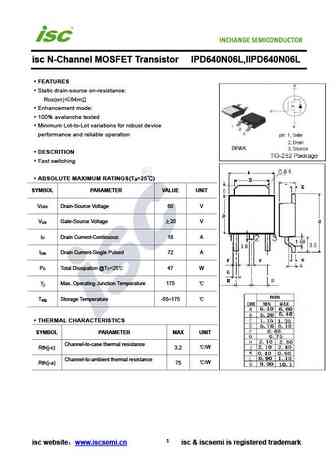
isc N-Channel MOSFET Transistor IPD640N06L,IIPD640N06L FEATURES Static drain-source on-resistance RDS(on) 64m Enhancement mode 100% avalanche tested Minimum Lot-to-Lot variations for robust device performance and reliable operation DESCRITION Fast switching ABSOLUTE MAXIMUM RATINGS(T =25 ) a SYMBOL PARAMETER VALUE UNIT V Drain-Source Voltage 60 V DSS V Ga
Другие MOSFET... 2SK845 , 2SK846 , 2SK857 , 2SK922 , 3N45 , 3N55 , 3N75 , 40N05 , IRFB31N20D , SUB45N05-20L , SUP45N05-20L , 45N06 , 45N20 , RFM4N35 , RFM4N40 , 4N60AS , 50N06FI .
History: 2SK3857MFV | SVS5N70F | PFB2N60 | STF13N60DM2 | STE38NB50 | STQ2HNK60Z-AP | WMN25N70EM
History: 2SK3857MFV | SVS5N70F | PFB2N60 | STF13N60DM2 | STE38NB50 | STQ2HNK60Z-AP | WMN25N70EM
🌐 : EN ES РУ

Список транзисторов
Обновления
MOSFET: ASU70R600E | ASU65R850E | ASU65R550E | ASU65R350E | ASR65R120EFD | ASR65R046EFD | ASQ65R046EFD | ASM65R280E | ASM60R330E | ASE70R950E | ASD80R750E | ASD70R950E | ASD70R600E | ASD70R380E | ASD65R850E | ASD65R550E
Popular searches
2sc2383 | c3198 transistor | irfb3607pbf datasheet | 60n60 | 2n5485 equivalent | 2sa1941 | 2sc485 | 2sd287