12N65H. Аналоги и основные параметры
Наименование производителя: 12N65H
Тип транзистора: MOSFET
Полярность: N
Предельные значения
Pd ⓘ - Максимальная рассеиваемая мощность: 140 W
|Vds|ⓘ - Максимально допустимое напряжение сток-исток: 650 V
|Vgs|ⓘ - Максимально допустимое напряжение затвор-исток: 30 V
|Id| ⓘ - Максимально допустимый постоянный ток стока: 12 A
Tj ⓘ - Максимальная температура канала: 150 °C
Электрические характеристики
tr ⓘ - Время нарастания: 28 ns
Cossⓘ - Выходная емкость: 195 pf
RDSonⓘ - Сопротивление сток-исток открытого транзистора: 0.7 Ohm
Тип корпуса: TO262
Аналог (замена) для 12N65H
- подборⓘ MOSFET транзистора по параметрам
12N65H даташит
kia12n65h.pdf
12A 650V 12N65H N-CHANNELMOSFET KIA KIA KIA SEMICONDUCTORS SEMICONDUCTORS SEMICONDUCTORS 1.Description The KIA12N65H N-Channel enhancement mode silicon gate power MOSFET is designed for high voltage, high speed power switching applications such as high efficiency switched mode power supplies, active power factor correction, electronic lamp ballasts based on half bridge topology.
tma12n65h tmp12n65h.pdf
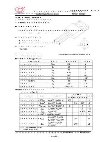
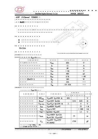
TMA12N65H, TMP12N65H Wuxi Unigroup Microelectronics Company 650V N-Channel MOSFET FEATURES Fast switching 100% avalanche tested Improved dv/dt capability APPLICATIONS Switch Mode Power Supply (SMPS) Uninterruptible Power Supply (UPS) Power Factor Correction (PFC) Device Marking and Package Information Device Package Marking TMA12N65H TO-220F A1
svf12n65f svf12n65t.pdf
SVF12N65T/F_Datasheet 12A, 650V N-CHANNEL MOSFET GENERAL DESCRIPTION SVF12N65T/F is an N-channel enhancement mode power MOS field effect transistor which is produced using Silan proprietary F-CellTM structure VDMOS technology. The improved planar stripe cell and the improved guard ring terminal have been especially tailored to minimize on-state resistance, provide superior switch
fqp12n65c fqpf12n65c.pdf
12N65 Series N-Channel MOSFET 12A, 650V, N H FQP12N65C H12N65P P TO-220AB 12N65 HAOHAI 50Pcs 1000Pcs 5000Pcs FQPF12N65C H12N65F F TO-220FP 12N65 Series Pin Assignment Features ID=12A Originative New Des
jcs12n65t.pdf
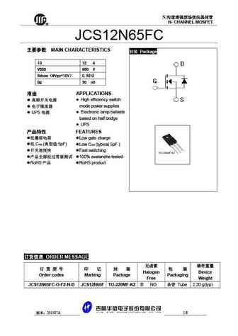
N R N-CHANNEL MOSFET JCS12N65T Package MAIN CHARACTERISTICS ID 12 A VDSS 650 V Rdson @Vgs=10V 0.78 Qg 39 nC APPLICATIONS High efficiency switch mode power supplies Electronic lamp ballasts UPS based on half bridge UPS FEA
12n65kl-t 12n65kg-t.pdf

UNISONIC TECHNOLOGIES CO., LTD 12N65K-MT Power MOSFET 12A, 650V N-CHANNEL POWER MOSFET DESCRIPTION The UTC 12N65K-MT are N-Channel enhancement mode power field effect transistors (MOSFET) which are produced by using UTC s proprietary, planar stripe and DMOS technology. These devices are suited for high efficiency switch mode power supply. To minimize on-state resistance,
sty112n65m5.pdf
STY112N65M5 N-channel 650 V, 0.019 , 96 A, MDmesh V Power MOSFET Max247 Features VDSS Order code RDS(on) max ID @TjMAX STY112N65M5 710 V
std12n65m2.pdf
STD12N65M2 N-channel 650 V, 0.42 typ., 8 A MDmesh M2 Power MOSFET in a DPAK package Datasheet - production data Features Order code V R max. I DS DS(on) D STD12N65M2 650 V 0.5 8 A Extremely low gate charge Excellent output capacitance (COSS) profile DPAK (TO-252) 100% avalanche tested Zener-protected Figure 1 Internal schematic diagram Applicatio
stl12n65m2.pdf
STL12N65M2 N-channel 650 V, 0.62 typ., 5 A MDmesh M2 Power MOSFET in a PowerFLAT 5x6 HV package Datasheet - production data Features Order code V R max. I P DS DS(on) D TOT STL12N65M2 650 V 0.75 5 A 48 W 1 Extremely low gate charge 2 3 Excellent output capacitance (COSS) profile 4 100% avalanche tested Zener-protected PowerFLAT 5x6 HV Ap
std12n65m5 stf12n65m5 sti12n65m5 stp12n65m5 stu12n65m5.pdf
STD12N65M5, STF12N65M5, STI12N65M5 STP12N65M5, STU12N65M5 N-channel 650 V, 0.39 , 8.5 A MDmesh V Power MOSFET DPAK, I2PAK, TO-220FP, TO-220, IPAK Features VDSS @ RDS(on) Type ID PTOT 3 TJmax max 2 3 1 2 1 STD12N65M5 8.5 A 70 W IPAK TO-220 STF12N65M5 8.5 A(1) 25 W 3 STI12N65M5 710 V
stl12n65m5.pdf
STL12N65M5 N-channel 650 V, 0.475 typ., 8.5 A MDmesh V Power MOSFET in a PowerFLAT 5x6 HV package Datasheet - production data Features Order code VDSS RDS(on) max ID STL12N65M5 710 V 0.530 8.5 A Outstanding RDS(on)*area 1 Extremely large avalanche performance 2 3 Gate charge minimized 4 TM Very low intrinsic capacitance PowerFLAT 5x6 HV 100% ava
stf12n65m2.pdf
STF12N65M2 N-channel 650 V, 0.42 typ., 8 A MDmesh M2 Power MOSFET in a TO-220FP package Datasheet - production data Features Order code VDS RDS(on) max ID STF12N65M2 650 V 0.5 8 A Extremely low gate charge Excellent output capacitance (Coss) profile 100% avalanche tested 3 2 Zener-protected 1 Applications TO-220FP Switching applications Figure
sihp12n65e.pdf
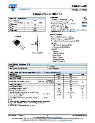
SiHP12N65E www.vishay.com Vishay Siliconix E Series Power MOSFET FEATURES PRODUCT SUMMARY Low figure-of-merit (FOM) Ron x Qg VDS (V) at TJ max. 700 Low input capacitance (Ciss) RDS(on) max. at 25 C ( ) VGS = 10 V 0.38 Reduced switching and conduction losses Qg max. (nC) 70 Ultra low gate charge (Qg) Qgs (nC) 9 Avalanche energy rated (UIS) Qgd (nC) 16 M
sihf12n65e.pdf
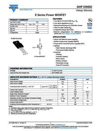
SiHF12N65E www.vishay.com Vishay Siliconix E Series Power MOSFET FEATURES PRODUCT SUMMARY Low figure-of-merit (FOM) Ron x Qg VDS (V) at TJ max. 700 Low input capacitance (Ciss) RDS(on) max. at 25 C ( ) VGS = 10 V 0.38 Reduced switching and conduction losses Qg max. (nC) 70 Ultra low gate charge (Qg) Qgs (nC) 9 Avalanche energy rated (UIS) Qgd (nC) 16 M
sihb12n65e.pdf
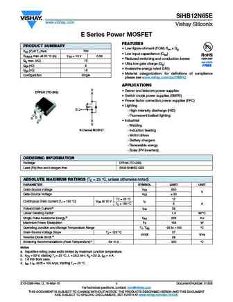
SiHB12N65E www.vishay.com Vishay Siliconix E Series Power MOSFET FEATURES PRODUCT SUMMARY Low figure-of-merit (FOM) Ron x Qg VDS (V) at TJ max. 700 Low input capacitance (Ciss) RDS(on) max. at 25 C ( ) VGS = 10 V 0.38 Reduced switching and conduction losses Qg max. (nC) 70 Ultra low gate charge (Qg) Qgs (nC) 9 Avalanche energy rated (UIS) Qgd (nC) 16 M
ixta12n65x2 ixth12n65x2 ixtp12n65x2.pdf
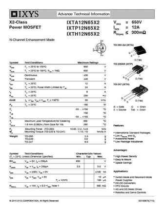
Advance Technical Information X2-Class VDSS = 650V IXTA12N65X2 Power MOSFET ID25 = 12A IXTP12N65X2 RDS(on) 300m IXTH12N65X2 N-Channel Enhancement Mode TO-263 AA (IXTA) G S D (Tab) Symbol Test Conditions Maximum Ratings TO-220AB (IXTP) VDSS TJ = 25 C to 150 C 650 V VDGR TJ = 25 C to 150 C, RGS = 1M 650 V VGSS Continuous 30
ixfp12n65x2m ixfp12n65x2 ixfa12n65x2 ixfh12n65x2.pdf
X2-Class HiPERFET VDSS = 650V IXFA12N65X2 Power MOSFET ID25 = 12A IXFP12N65X2 RDS(on) 310m IXFH12N65X2 N-Channel Enhancement Mode Avalanche Rated TO-263 (IXFA) G S D (Tab) Symbol Test Conditions Maximum Ratings TO-220 (IXFP) VDSS TJ = 25 C to 150 C 650 V VDGR TJ = 25 C to 150 C, RGS = 1M 650 V VGSS Continuous 30 V VGSM Tr
12n65kl-ta3-t 12n65kg-ta3-t 12n65kl-tf1-t 12n65kg-tf1-t 12n65kl-tf2-t 12n65kg-tf2-t 12n65kl-tf3-t 12n65kg-tf3-t 12n65kl-tq2-t 12n65kg-tq2-t 12n65kl-tq2-r 12n65kg-tq2-r.pdf
UNISONIC TECHNOLOGIES CO., LTD 12N65K-MT Power MOSFET 12A, 650V N-CHANNEL POWER MOSFET DESCRIPTION The UTC 12N65K-MT are N-Channel enhancement mode power field effect transistors (MOSFET) which are produced by using UTC s proprietary, planar stripe and DMOS technology. These devices are suited for high efficiency switch mode power supply. To minimize on-state resistance,
cjp12n65.pdf
JIANGSU CHANGJIANG ELECTRONICS TECHNOLOGY CO., LTD TO-220-3L Plastic-Encapsulate MOSFETS CJP12N65 N-Channel Power MOSFET TO-220-3L GENERAL DESCRIPTION This advanced high voltage MOSFET is designed to stand high energy in the avalanche mode and switch efficiently. This new high energy device also offers a drain-to-source diode fast recovery time. Designed for high voltage, hig
cjpf12n65.pdf
JIANGSU CHANGJIANG ELECTRONICS TECHNOLOGY CO., LTD TO-220F Plastic-Encapsulate MOSFETS CJPF12N65 N-Channel Power MOSFET TO-220F GENERAL DESCRIPTION This advanced high voltage MOSFET is designed to stand high energy in the avalanche mode and switch efficiently. This new high energy device also offers a drain-to-source diode fast recovery time. Designed for high voltage, high s
cep12n65 ceb12n65 cef12n65.pdf
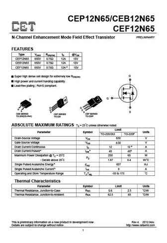
CEP12N65/CEB12N65 CEF12N65 PRELIMINARY N-Channel Enhancement Mode Field Effect Transistor FEATURES Type VDSS RDS(ON) ID @VGS CEP12N65 650V 0.73 12A 10V CEB12N65 650V 0.73 12A 10V CEF12N65 650V 0.73 12A d 10V D Super high dense cell design for extremely low RDS(ON). High power and current handing capability. Lead-free plating ; RoHS compliant. G S CEB SERIES CEP SERIES C
wnm12n65-f.pdf
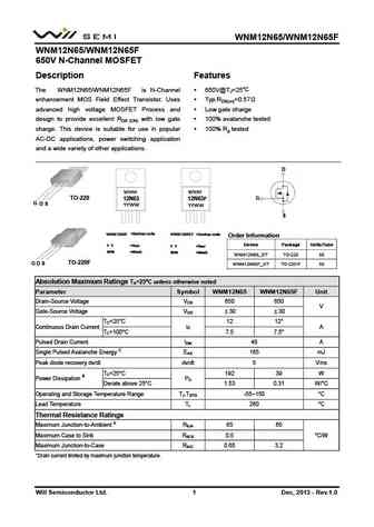
WNM12N65/WNM12N65F WNM12N65/WNM12N65F 650V N-Channel MOSFET Description Features C The WNM12N65/WNM12N65F is N-Channel 650V@TJ=25 enhancement MOS Field Effect Transistor. Uses Typ.RDS(on)=0.57 advanced high voltage MOSFET Process and Low gate charge design to provide excellent RDS (ON) with low gate 100% avalanche tested charge. This device is suitable for use in p
h12n65.pdf
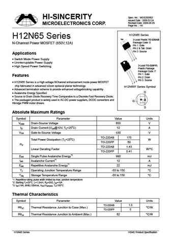
Spec. No. MOS200902 HI-SINCERITY Issued Date 2009.03.24 Revised Date 2009.08.05 MICROELECTRONICS CORP. Page No. 1/6 H12N65 Series H12N65 Series Tab 3-Lead Plastic TO-220AB Package Code E N-Channel Power MOSFET (650V,12A) Pin 1 Gate Pin 2 & Tab Drain Pin 3 Source Applications 3 Switch Mode Power Supply 2 1 Uninterruptable Power Supply 3-L
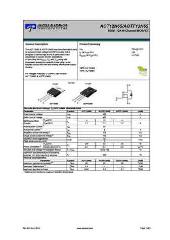
aob12n65l.pdf

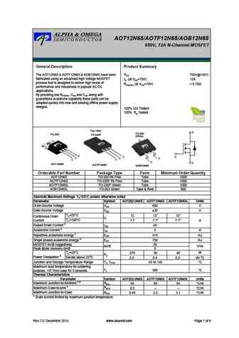
AOT12N65/AOTF12N65/AOB12N65 650V, 12A N-Channel MOSFET General Description Product Summary VDS 750V@150 The AOT12N65 & AOTF12N65 & AOB12N65 have been fabricated using an advanced high voltage MOSFET ID (at VGS=10V) 12A process that is designed to deliver high levels of RDS(ON) (at VGS=10V)
aotf12n65.pdf
AOT12N65/AOTF12N65 650V, 12A N-Channel MOSFET General Description Product Summary VDS 750V@150 The AOT12N65 & AOTF12N65 have been fabricated using an advanced high voltage MOSFET process that is ID (at VGS=10V) 12A designed to deliver high levels of performance and RDS(ON) (at VGS=10V)
aot12n65 aotf12n65 aotf12n65l aob12n65l.pdf

AOT12N65/AOTF12N65/AOTF12N65L/AOB12N65L 650V, 12A N-Channel MOSFET General Description Product Summary VDS 750V@150 The AOT12N65 & AOTF12N65 & AOTF12N65L & AOB12N65L have been fabricated using an advanced ID (at VGS=10V) 12A high voltage MOSFET process that is designed to deliver RDS(ON) (at VGS=10V)
aot12n65 aotf12n65 aob12n65.pdf
AOT12N65/AOTF12N65/AOB12N65 650V, 12A N-Channel MOSFET General Description Product Summary VDS 750V@150 The AOT12N65 & AOTF12N65 & AOB12N65 have been fabricated using an advanced high voltage MOSFET ID (at VGS=10V) 12A process that is designed to deliver high levels of RDS(ON) (at VGS=10V)
aowf12n65.pdf
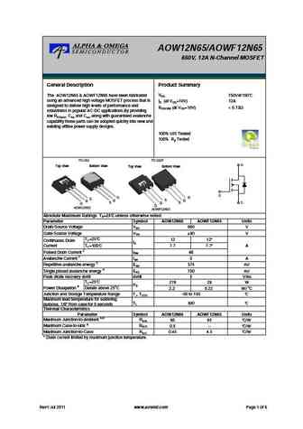
AOW12N65/AOWF12N65 650V, 12A N-Channel MOSFET General Description Product Summary VDS 750V@150 The AOW12N65 & AOWF12N65 have been fabricated using an advanced high voltage MOSFET process that is ID (at VGS=10V) 12A designed to deliver high levels of performance and RDS(ON) (at VGS=10V)
aow12n65.pdf

AOW12N65/AOWF12N65 650V, 12A N-Channel MOSFET General Description Product Summary VDS 750V@150 The AOW12N65 & AOWF12N65 have been fabricated using an advanced high voltage MOSFET process that is ID (at VGS=10V) 12A designed to deliver high levels of performance and RDS(ON) (at VGS=10V)
aot12n65.pdf

AOT12N65/AOTF12N65 650V, 12A N-Channel MOSFET General Description Product Summary VDS 750V@150 The AOT12N65 & AOTF12N65 have been fabricated using an advanced high voltage MOSFET process that is ID (at VGS=10V) 12A designed to deliver high levels of performance and RDS(ON) (at VGS=10V)
am12n65pcfm.pdf
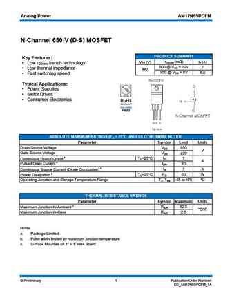
Analog Power AM12N65PCFM N-Channel 650-V (D-S) MOSFET PRODUCT SUMMARY Key Features rDS(on) (m ) VDS (V) ID (A) Low r trench technology DS(on) 800 @ VGS = 10V 7 Low thermal impedance 650 850 @ VGS = 6V 6.5 Fast switching speed Typical Applications Power Supplies Motor Drives Consumer Electronics ABSOLUTE MAXIMUM RATINGS (TA = 25 C UNLESS OTH
am12n65p.pdf
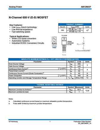
Analog Power AM12N65P N-Channel 650-V (D-S) MOSFET PRODUCT SUMMARY Key Features rDS(on) (m ) VDS (V) ID (A) Low r trench technology DS(on) 800 @ VGS = 10V Low thermal impedance 650 12a 850 @ VGS = 6V Fast switching speed Typical Applications White LED boost converters Automotive Systems DRAIN connected Industrial DC/DC Conversion Circuits
afn12n65t220ft afn12n65t220t.pdf
AFN12N65 Alfa-MOS 650V / 12A N-Channel Technology Enhancement Mode MOSFET General Description Features AFN12N65 is an N-channel enhancement mode Power 650V/6A,RDS(ON)=0.8 (MAX)@VGS=10V MOSFET which is produced using VDMOS technology. The Low gate charge improved planar stripe cell and the improved guard ring Low Crss terminal have been especially tailored to minimize on-stat
sif12n65c.pdf
Shenzhen SI Semiconductors Co., LTD. Product Specification Shenzhen SI Semiconductors Co., LTD. Product Specification Shenzhen SI Semiconductors Co., LTD. Product Specification Shenzhen SI Semiconductors Co., LTD. Product Specification N- MOS / N-CHANNEL POWER MOSFET SIF12N65C N- MOS / N-CHANNEL POWER MOSFET SIF12N65C
jcs12n65fei jcs12n65bei jcs12n65sei jcs12n65cei.pdf
N R N-CHANNEL MOSFET JCS12N65EI Package MAIN CHARACTERISTICS ID 12A VDSS 650V Rdson-max 0.9 Vgs=10V Qg-Typ 30nC APPLICATIONS High efficiency switch mode power supplies Electronic lamp ballasts LED based on half bridge LE
jcs12n65bt jcs12n65st jcs12n65ct jcs12n65ft.pdf
N R N-CHANNEL MOSFET JCS12N65T Package MAIN CHARACTERISTICS ID 12.0A VDSS 650 V Rdson-max 0.78 @Vgs=10V Qg-typ 39 nC APPLICATIONS High efficiency switch mode power supplies Electronic lamp ballasts LED based on half bridge
mtn12n65fp.pdf
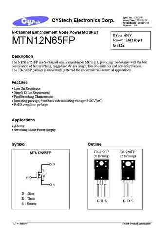
Spec. No. C802FP Issued Date 2010.01.08 CYStech Electronics Corp. Revised Date 2012.01.13 Page No. 1/9 N-Channel Enhancement Mode Power MOSFET BVDSS 650V RDS(ON) 0.6 (typ.) MTN12N65FP ID 12A Description The MTN12N65FP is a N-channel enhancement-mode MOSFET, providing the designer with the best combination of fast switching, ruggedized device design, low on
12n65a 12n65af.pdf
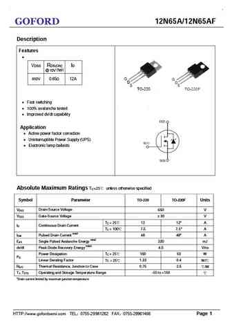
12N65A/12N65AF GOFORD Description Features VDSS RDS(ON) ID @ 10V (typ) 12A 650V 0.65 Fast switching 100% avalanche tested Improved dv/dt capability Application Active power factor correction Uninterruptible Power Supply (UPS) Electronic lamp ballasts Absolute Maximum Ratings TC=25 unless otherwise specified Symbol Parameter TO-220
ssf12n65f.pdf
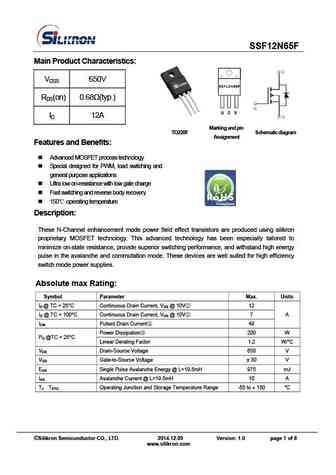
SSF12N65F Main Product Characteristics VDSS 650V RDS(on) 0.68 (typ.) ID 12A Marking and pin TO220F Schematic diagram Assignment Features and Benefits Advanced MOSFET process technology Special designed for PWM, load switching and general purpose applications Ultra low on-resistance with low gate charge Fast switching and reverse body recovery
brf12n65.pdf
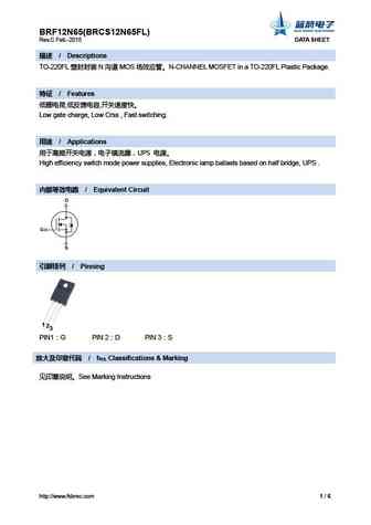
BRF12N65(BRCS12N65FL) Rev.C Feb.-2015 DATA SHEET / Descriptions TO-220FL N MOS N-CHANNEL MOSFET in a TO-220FL Plastic Package. / Features , , Low gate charge, Low Crss , Fast switching. / Applications UPS High efficiency sw
brcs12n65bd.pdf
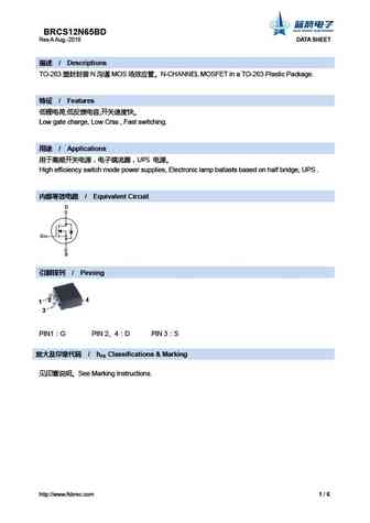
BRCS12N65BD Rev.A Aug.-2018 DATA SHEET / Descriptions TO-263 N MOS N-CHANNEL MOSFET in a TO-263 Plastic Package. / Features , , Low gate charge, Low Crss , Fast switching. / Applications UPS High efficiency switch mode pow
brfl12n65.pdf
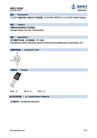
BRFL12N65 Rev.F Nov.-2017 DATA SHEET / Descriptions TO-220FL N MOS N-CHANNEL MOSFET in a TO-220FL Plastic Package. / Features , , Low gate charge, Low Crss , Fast switching. / Applications UPS High efficiency switch mode po
cs12n65f a9r.pdf
Silicon N-Channel Power MOSFET R CS12N65F A9R General Description VDSS 650 V CS12N65F A9R, the silicon N-channel Enhanced ID 12 A PD(TC=25 ) 42 W VDMOSFETs, is obtained by the self-aligned planar Technology RDS(ON)Typ 0.66 which reduce the conduction loss, improve switching performance and enhance the avalanche energy. The transistor can be used in various p
cs12n65 a8r.pdf
Silicon N-Channel Power MOSFET R CS12N65 A8R General Description VDSS 650 V CS12N65 A8R, the silicon N-channel Enhanced ID 12 A PD(TC=25 ) 150 W VDMOSFETs, is obtained by the self-aligned planar Technology RDS(ON)Typ 0.66 which reduce the conduction loss, improve switching performance and enhance the avalanche energy. The transistor can be used in various po
cs12n65f a9h.pdf
Silicon N-Channel Power MOSFET R CS12N65F A9H VDSS 650 V General Description ID 12 A CS12N65F A9H, the silicon N-channel Enhanced PD (TC=25 ) 55 W VDMOSFETs, is obtained by the self-aligned planar RDS(ON)Typ 0.54 Technology which reduce the conduction loss, improve switching performance and enhance the avalanche energy. The transistor can be used in various
cs12n65 a8h.pdf
Silicon N-Channel Power MOSFET R CS12N65 A8H VDSS 650 V General Description ID 12 A CS12N65 A8H, the silicon N-channel Enhanced PD (TC=25 ) 140 W VDMOSFETs, is obtained by the self-aligned planar RDS(ON)Typ 0.54 Technology which reduce the conduction loss, improve switching performance and enhance the avalanche energy. The transistor can be used in various p
pfp12n65 pff12n65.pdf
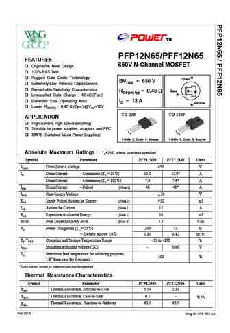
PFP12N65/PFF12N65 FEATURES 650V N-Channel MOSFET Originative New Design 100% EAS Test Rugged Gate Oxide Technology Drain BVDSS = 650 V Extremely Low Intrinsic Capacitances Remarkable Switching Characteristics Gate RDS(on) typ = 0.46 Unequalled Gate Charge 48 nC (Typ.) E
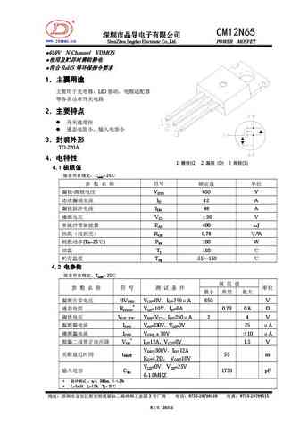
cm12n65a to220a.pdf
R CM12N65A www.jdsemi.cn ShenZhen Jingdao Electronic Co.,Ltd. POWER MOSFET 650V N-Channel VDMOS RoHS 1 LD E 2 3
cm12n65 to220a.pdf
R CM12N65 www.jdsemi.cn ShenZhen Jingdao Electronic Co.,Ltd. POWER MOSFET 650V N-Channel VDMOS RoHS
cm12n65f.pdf
R CM12N65F www.jdsemi.cn ShenZhen Jingdao Electronic Co.,Ltd. POWER MOSFET 650V N-Channel VDMOS RoHS 1 LD E 2 1 2
ftk12n65p f dd.pdf
SEMICONDUCTOR FTK12N65P/F/DD TECHNICAL DATA 12 Amps, 650 Volts N-CHANNEL MOSFET DESCRIPTION These N-Channel enhancement mode power field effect P Transistors are produced using planar stripe, DMOS technology. 1 This advanced technology has been especially tailored to minimize on - state resistance , provide superior TO-220 switching performance,and Withstand high energy pulse i
f12n65.pdf
F12N65 12A 650V N-channel Enhancement Mode Power MOSFET 1 Description These N-channel enhanced vdmosfets, is obtained by the self-aligned V DSS = 650V planar technology which reduce the conduction loss, improve switching I = 12.0A D performance and enhance the avalanche energy. Which accords with the RoHS standard. TO-220F provides insulation voltage rated at 2000V R DS(on) TYP)
12n65.pdf
12N65 12A 650V N-channel Enhancement Mode Power MOSFET 1 Description These N-channel enhanced vdmosfets, is obtained by the self-aligned V DSS = 650V planar technology which reduce the conduction loss, improve switching I = 12.0A D performance and enhance the avalanche energy. Which accords with the RoHS standard. R DS(on) TYP) =0.66 2 Features Fast switching ESD imp
kx12n65f.pdf
DIP Type MOSFET N-Channel MOSFET KX12N65F TO-220F Unit mm 10.16 0.20 3.18 0.10 2.54 0.20 (7.00) (0.70) Features VDS (V) = 650V (1.00x45 ) ID = 12 A (VGS = 10V) RDS(ON) 850m (VGS = 10V) 1 2 3 MAX1.47 High ruggedness 0.80 0.10 D #1 0.35 0.10 +0.10 0.50 0.05 2.76 0.20 2.54TYP 2.54TYP [2.54 0.20] [2.54 0.20] 9.40 0.20 G 1. Gate 2. Drain
svf12n65cf svf12n65ck svf12n65cs svf12n65ckl svf12n65cfq.pdf
SVF12N65CF/K/S/KL/FQ 12A 650V N SVF12N65CF/K/S/KL/FQ N MOS F-CellTM VDMOS A
svf12n65t svf12n65f.pdf
SVF12N65T/F 12A 650V N 2 SVF12N65T/F N MOS F-CellTM VDMOS 1 3
ms12n65.pdf
MS12N65 N-Channel Enhancement Mode Power MOSFET Description The MS12N65 is a N-channel enhancement-mode MOSFET, providing the designer with the best combination of fast switching, ruggedized device design, low on-resistance and cost effectiveness. The TO-220 package is universally preferred for all commercial-industrial applications Features Low gate charge ( typical 52n
msf12n65.pdf
MSF12N65 650V N-Channel MOSFET Description The MSF12N65 is a N-channel enhancement-mode MOSFET , providing the designer with the best combination of fast switching, ruggedized device design, low on-resistance and cost effectiveness. The TO-220F package is universally preferred for all commercial-industrial applications Features Low gate charge ( typical 52nC) High
ru12n65p.pdf
RU12N65P N-Channel Advanced Power MOSFET Features Pin Description 650V/12A, RDS (ON) =650m (Typ.)@VGS=10V Low Reverse Transfer Ultra Low Gate Charge 100% avalanche tested Lead Free and Green Devices Available (RoHS Compliant) Lead Free and Green Devices Available (RoHS Compliant) GD S TO220F D D D D D Applications D pp D AC/DC Power Conversion
wfp12n65.pdf
WFP12N65 WFP12N65 WFP12N65 WFP12N65 Silicon N-Channel MOSFET Features 12A,650V,RDS(on)(Max0.78 )@VGS=10V Ultra-low Gate Charge(Typical 51.7nC) Fast Switching Capability 100%Avalanche Tested Maximum Junction Temperature Range(150 ) General Description This Po wer MOS FE T is pro du ced usi ng Win se mi s adva nce d planar stripe, VDMOS technology. This late
sfp12n65.pdf
SFP12N65 SFP12N65 SFP12N65 SFP12N65 Silicon N-Channel MOSFET Silicon N-Channel MOSFET Silicon N-Channel MOSFET Silicon N-Channel MOSFET Features 12A,650V,RDS(on)(Max0.78 )@VGS=10V Ultra-low Gate Charge(Typical 30nC) Fast Switching Capability 100% Avalanche Tested Maximum Junction Temperature Range(150 ) General Description This Power MOSFET is produced usin
wfp12n65s.pdf
WFP12N65S Super-junction N-Channel Power MOSFET Features 12A,650V,R (Max0.30 )@V =10V DS(on) GS Ultra-low Gate charge(Typical 84.4nC) High EAS energy 100%Avalanche Tested RoHS Compliant Maximum Junction Temperature Range(150 ) General Description This Super-junction Power MOSFET is produced using Winsemi's employs a deep trench filling process t
wff12n65.pdf
WFF12N65 WFF12N65 WFF12N65 WFF12N65 Silicon N-Channel MOSFET Features 12A,650V,RDS(on)(Max0.78 )@VGS=10V Ultra-low Gate Charge(Typical 51.7nC) Fast Switching Capability 100%Avalanche Tested Maximum Junction Temperature Range(150 ) General Description This Power MOSFET is produced using Winsemi s advanced planar stripe, VDMOS technology. This latest technol
bl12n65-p bl12n65-a.pdf
BL12N65 Power MOSFET Power MOSFET Power MOSFET Power MOSFET 1 Description BL12N65, the silicon N-channel Enhanced MOSFETs, is obtained by advanced MOSFET technology which reduce the conduction loss, improve switching performance and enhance the avalanche energy. The transistor is suitable device for SMPS, high speed switching and general purpose application
bl12n65a-p bl12n65a-a.pdf
BL12N65A Power MOSFET Power MOSFET Power MOSFET Power MOSFET 1 Description BL12N65A, the silicon N-channel Enhanced MOSFETs, is obtained by advanced MOSFET technology which reduce the conduction loss, improve switching performance and enhance the avalanche energy. The transistor is suitable device for SMPS, high speed switching and general purpose applicati
fhp12n65c fhf12n65c.pdf
N N-CHANNEL MOSFET FHP12N65C/ FHF12N65C MAIN CHARACTERISTICS FEATURES Low gate charge ID 12A Crss ( 18pF) Low Crss (typical 18pF ) VDSS 650V Fast switching Rdson-typ 0.63 @Vgs=10V 100% 100% avalanche tested Qg-typ 52nC dv/dt I
hy12n65t.pdf
HY12N65T / HY12N65FT 650V / 12A 650V, RDS(ON)=0.8 @VGS=10V, ID=6.0A N-Channel Enhancement Mode MOSFET Features Low ON Resistance Fast Switching Low Gate Charge & Low CRSS Fully Characterized Avalanche Voltage and Current Specially Desigened for AC Adapter, Battery Charger and SMPS 1 1 2 2 In compliance with EU RoHs 2002/95/EC Directives G G 3 3 D D S S
jfpc12n65c.pdf
JFPC12N65C 650V N-Channel MOSFET General Description This Power MOSFET is produced using advanced planar stripe DMOS technology. This advanced technology has been especially tailored to minimize on-state resistance, provide superior switching performance, and withstand high energy pulse in the avalanche and commutation mode. These devices are well suited for high efficiency
jfpc12n65d.pdf
JFPC12N65D 650V N-Channel MOSFET General Description This Power MOSFET is produced using advanced planar stripe DMOS technology. This advanced technology has been especially tailored to minimize on-state resistance, provide superior switching performance, and withstand high energy pulse in the avalanche and commutation mode. These devices are well suited for high efficiency
slf12n65sv.pdf
SLF12N65SV 650V N-Channel MOSFET General Description Features This Power MOSFET is produced using Msemitek s advanced 12A*, 650V, RDS(on),typ =0.67 planar stripe DMOS technology. This advanced technology Low gate charge (Qg,typ = 33nC) has been especially tailored to minimize conduction loss, pro- Fast switching vide superior switching performance, and withstand high en-
slp12n65c slf12n65c.pdf
SLP12N65C / SLF12N65C 650V N-Channel MOSFET General Description Features This Power MOSFET is produced using Maple semi s - 12A, 650V, RDS(on) typ. = 0.6 @VGS = 10 V advanced planar stripe DMOS technology. - Low gate charge ( typical 47nC) This advanced technology has been especially tailored - High ruggedness to minimize on-state resistance, provide superior switching - Fast switching
ptp12n65 pta12n65.pdf
PTP12N65 PTA12N65 650V N-ch Planar MOSFET General Features BVDSS RDS(ON),typ. ID RoHS Compliant 650V 0.60 12A RDS(ON),typ.=0.60 @VGS=10V Low Gate Charge Minimize Switching Loss Fast Recovery Body Diode Applications Adaptor Charger G D S G D SMPS Standby Power S Ordering Information TO-220 TO-220F Part Number Package Brand
swf12n65d swu12n65d swp12n65d swb12n65d.pdf
SW12N65D N-channel Enhanced mode TO-220F/TO-262/TO-220/TO-263 MOSFET Features TO-220F TO-262 TO-220 TO-263 BVDSS 650V High ruggedness ID 12A Low RDS(ON) (Typ 0.7 )@VGS=10V RDS(ON) 0.7 Low Gate Charge (Typ 45nC) Improved dv/dt Capability 2 1 100% Avalanche Tested 1 1 1 2 2 2 2 3 Application Charger,LED,PC Power 3 3 3 1. Gate 2.
swmn12n65da.pdf
SW12N65DA N-channel Enhanced mode TO-220SF MOSFET TO-220SF Features BVDSS 650V ID 12A High ruggedness Low RDS(ON) (Typ 0.75 )@VGS=10V RDS(ON) 0.75 Low Gate Charge (Typ 43nC) Improved dv/dt Capability 2 1 100% Avalanche Tested 2 3 Application LED, Charger, PC Power 1 1. Gate 2. Drain 3. Source 3 General Description Th
swmn12n65d swy12n65d.pdf
SW12N65D N-channel Enhanced mode TO-220SF/TO-220FT MOSFET TO-220SF TO-220FT BVDSS 650V Features ID 12A High ruggedness RDS(ON) 0.66 Low RDS(ON) (Typ 0.66 )@VGS=10V Low Gate Charge (Typ 41nC) 2 Improved dv/dt Capability 1 1 100% Avalanche Tested 2 1 2 3 3 Application LED , Charger, PC Power 1. Gate 2. Drain 3. Source
sw12n65d swf12n65d swu12n65d swp12n65d swb12n65d.pdf

SW12N65D N-channel Enhanced mode TO-220F/TO-262/TO-220/TO-263 MOSFET Features TO-262 TO-220F TO-220 TO-263 BVDSS 650V High ruggedness ID 12A Low RDS(ON) (Typ 0.7 )@VGS=10V RDS(ON) 0.7 Low Gate Charge (Typ 45nC) Improved dv/dt Capability 2 1 100% Avalanche Tested 1 1 1 2 2 2 2 3 Application Charge,LED,PC Power 3 3 3 1. Gate 2
srm12n65.pdf
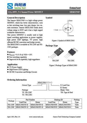
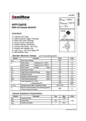
Datasheet 12A, 650V, N-Channel Power MOSFET SRM12N65 General Description Symbol The Sanrise SRM12N65 is a high voltage power MOSFET, which has better characteristics, such as fast switching time, low gate charge, low on- state resistance. Sanrise SRM12N65 break down voltage rating is 650V and it has a high rugged avalanche characteristics. This power MOSFET is usually used at hi
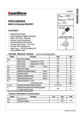
hfp12n65s.pdf
Aug 2009 BVDSS = 650 V RDS(on) typ = 0.67 HFP12N65S ID = 12 A 650V N-Channel MOSFET TO-220 FEATURES Originative New Design 1 2 3 Superior Avalanche Rugged Technology 1.Gate 2. Drain 3. Source Robust Gate Oxide Technology Very Low Intrinsic Capacitances Excellent Switching Characteristics Unrivalled Gate Charge 38 nC (Typ.) Unrivalled Gate Charge 38 nC (Typ ) Ext
hfs12n65sa.pdf
July 2021 BVDSS = 650 V RDS(on) typ = 0.67 HFS12N65SA ID = 12 A 650V N-Channel MOSFET TO-220F FEATURES 1 Originative New Design 2 3 Superior Avalanche Rugged Technology 1.Gate 2. Drain 3. Source Robust Gate Oxide Technology Very Low Intrinsic Capacitances Excellent Switching Characteristics Unrivalled Gate Charge 41 nC (Typ.) Extended Safe Ope
hfs12n65s.pdf
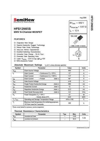
Aug 2009 BVDSS = 650 V RDS(on) typ = 0.67 HFS12N65S ID = 12 A 650V N-Channel MOSFET TO-220F FEATURES 1 Originative New Design 2 3 Superior Avalanche Rugged Technology 1.Gate 2. Drain 3. Source Robust Gate Oxide Technology Very Low Intrinsic Capacitances Excellent Switching Characteristics Unrivalled Gate Charge 38 nC (Typ.) Unrivalled Gate Charge 38 nC (Typ ) E
hfp12n65u.pdf
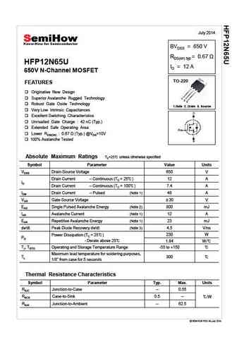
July 2014 BVDSS = 650 V RDS(on) typ = 0.67 HFP12N65U ID = 12 A 650V N-Channel MOSFET TO-220 FEATURES Originative New Design Superior Avalanche Rugged Technology 1 2 3 Robust Gate Oxide Technology 1.Gate 2. Drain 3. Source Very Low Intrinsic Capacitances Excellent Switching Characteristics Unrivalled Gate Charge 42 nC (Typ.) Extended Safe Operating Area Lo
hfs12n65js.pdf
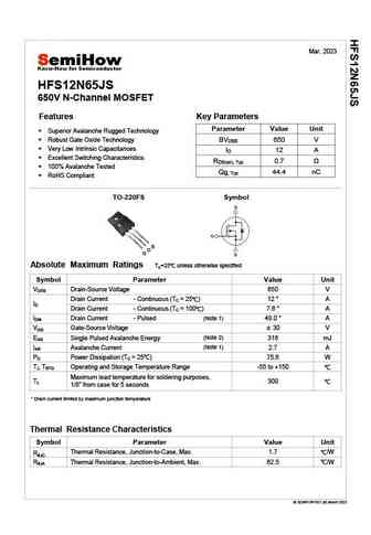
Mar. 2023 HFS12N65JS 650V N-Channel MOSFET Features Key Parameters Parameter Value Unit Superior Avalanche Rugged Technology BVDSS 650 V Robust Gate Oxide Technology Very Low Intrinsic Capacitances ID 12 A Excellent Switching Characteristics RDS(on), Typ 0.7 100% Avalanche Tested Qg, Typ 44.4 nC RoHS Compliant TO-220FS Symbol S D G Absolute Maximum
hfs12n65u.pdf
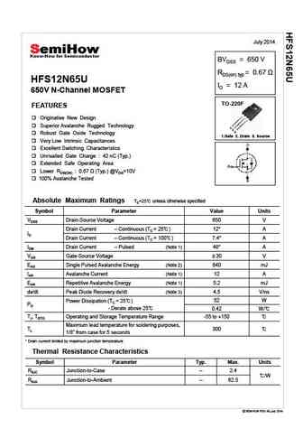
July 2014 BVDSS = 650 V RDS(on) typ = 0.67 HFS12N65U ID = 12 A 650V N-Channel MOSFET TO-220F FEATURES Originative New Design Superior Avalanche Rugged Technology 1 2 3 Robust Gate Oxide Technology 1.Gate 2. Drain 3. Source Very Low Intrinsic Capacitances Excellent Switching Characteristics Unrivalled Gate Charge 42 nC (Typ.) Extended Safe Operating Area Lo
tsp12n65m tsf12n65m.pdf
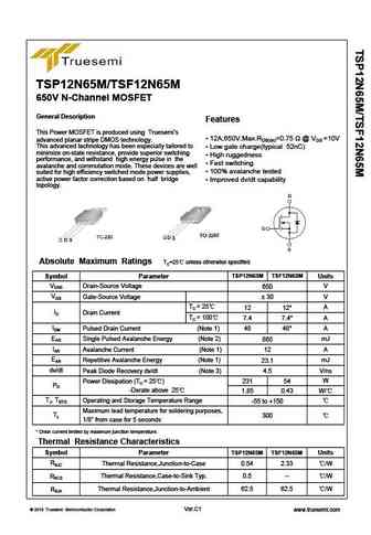
TSP12N65M/TSF12N65M 650V N-Channel MOSFET General Description Features This Power MOSFET is produced using Truesemi s 12A,650V,Max.RDS(on)=0.75 @ VGS =10V advanced planar stripe DMOS technology. This advanced technology has been especially tailored to Low gate charge(typical 52nC) minimize on-state resistance, provide superior switching High ruggedness performance, a
qm12n65f.pdf
QM12N65F 1 2011-03-03 - 1 - N-Ch 650V Fast Switching MOSFETs General Description Product Summery The QM12N65F is the highest performance N-ch MOSFETs with specialized high voltage BVDSS RDSON ID technology, which provide excellent RDSON and 650V 0.8 12A gate charge for most of the SPS, Charger ,Adapter and lighting applications . Applications The QM12N65F me
qm12n65p.pdf
QM12N65P 1 2011-03-03 - 1 - N-Ch 650V Fast Switching MOSFETs General Description Product Summery The QM12N65P is the highest performance N-ch MOSFETs with specialized high voltage BVDSS RDSON ID technology, which provide excellent RDSON and 650V 0.8 12A gate charge for most of the SPS, Charger ,Adapter and lighting applications . Applications The QM12N65P me
qm12n65b.pdf
QM12N65B 1 2011-03-03 - 1 - N-Ch 650V Fast Switching MOSFETs General Description Product Summery The QM12N65B is the highest performance N-ch MOSFETs with specialized high voltage BVDSS RDSON ID technology, which provide excellent RDSON and 650V 0.8 12A gate charge for most of the SPS, Charger ,Adapter and lighting applications . Applications The QM12N65B m
wml12n65d1b wmk12n65d1b.pdf
WML12N65D1B WMK12N65D1B 650V 12A 0.58 N-ch Power MOSFET Description TO-220 TO-220F WMOSTM D1 is Wayon s 1st generation VDMOS family that is dramatic reduction in on-resistance and ultra-low gate charge for applications requiring high power density and high efficiency. And it is very robust and RoHS compliant. G Features D G S D S V =700V@T DS jmax Typ.R =0.58 @V =1
wml12n65d1 wmk12n65d1.pdf

WML12N65D1 WMK12N65D1 650V 12A 0.58 N-ch Power MOSFET Description TO-220 TO-220F WMOSTM D1 is Wayon s 1st generation VDMOS family that is dramatic reduction in on-resistance and ultra-low gate charge for applications requiring high power density and high efficiency. And it is very robust and RoHS compliant. G Features D G S D S V =700V@T DS jmax Typ.R =0.58 @V =10V
cs12n65fa9h.pdf

Silicon N-Channel Power MOSFET R CS12N65F A9H VDSS 650 V General Description ID 12 A CS12N65F A9H, the silicon N-channel Enhanced PD (TC=25 ) 55 W VDMOSFETs, is obtained by the self-aligned planar RDS(ON)Typ 0.54 Technology which reduce the conduction loss, improve switching performance and enhance the avalanche energy. The transistor can be used in various
cs12n65a8h.pdf

Silicon N-Channel Power MOSFET R CS12N65 A8H VDSS 650 V General Description ID 12 A CS12N65 A8H, the silicon N-channel Enhanced PD (TC=25 ) 140 W VDMOSFETs, is obtained by the self-aligned planar RDS(ON)Typ 0.54 Technology which reduce the conduction loss, improve switching performance and enhance the avalanche energy. The transistor can be used in various p
cs12n65fa9r.pdf

Silicon N-Channel Power MOSFET R CS12N65F A9R General Description VDSS 650 V CS12N65F A9R, the silicon N-channel Enhanced ID 12 A PD(TC=25 ) 42 W VDMOSFETs, is obtained by the self-aligned planar Technology RDS(ON)Typ 0.66 which reduce the conduction loss, improve switching performance and enhance the avalanche energy. The transistor can be used in various p
cs12n65f cs12n65p.pdf
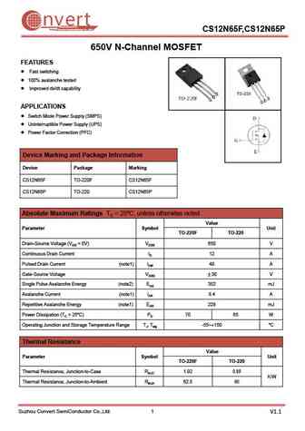
nvert Suzhou Convert Semiconductor Co ., Ltd. CS12N65F,CS12N65P 650V N-Channel MOSFET FEATURES Fast switching 100% avalanche tested Improved dv/dt capability APPLICATIONS Switch Mode Power Supply (SMPS) Uninterruptible Power Supply (UPS) Power Factor Correction (PFC) Device Marking and Package Information Device Package Marking CS12N65F TO-220F CS12N65F CS
cs12n65ff.pdf
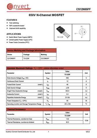
nvert Suzhou Convert Semiconductor Co ., Ltd. CS12N65FF 650V N-Channel MOSFET FEATURES Fast switching 100% avalanche tested Improved dv/dt capability APPLICATIONS Switch Mode Power Supply (SMPS) Uninterruptible Power Supply (UPS) Power Factor Correction (PFC) Device Marking and Package Information Device Package Marking CS12N65FF TO-220F CS12N65FF Absolute
fir12n65fg.pdf
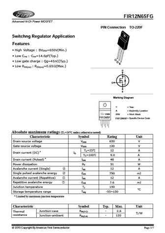
FIR12N65FG Advanced N-Ch Power MOSFET PIN Connection TO-220F Switchng Regulator Application Features High Voltage BVDSS=650V(Min.) Low Crss Crss=14.6pF(Typ.) G Low gate charge Qg=41nC(Typ.) D S Low RDS(on) RDS(on)=0.65 (Max.) D G S Marking Diagram Y = Year A = Assembly Location YAWW WW = Work Week FIR12N65F FIR12N65F = Specific Device C
smf12n65.pdf
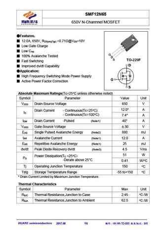
SMF12N65 650V N-Channnel MOSFET Features 12.0A, 650V, R =0.71 @V =10V DS(on)(Typ) GS Low Gate Charge Low C rss 100% Avalanche Tested Fast Switching Improved dv/dt Capability Application High Frequency Switching Mode Power Supply Active Power Factor Correction Absolute Maximum Ratings(Tc=25 C unless otherwise noted) Symbol Parameter Va
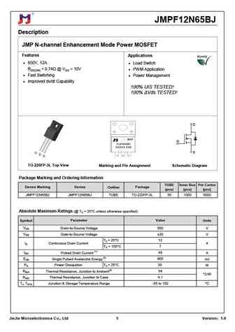
jmpf12n65bj.pdf
JMPF12N65BJ Description JMP N-channel Enhancement Mode Power MOSFET Features Applications 650V, 12A Load Switch RDS(ON)
jmpc12n65bj.pdf
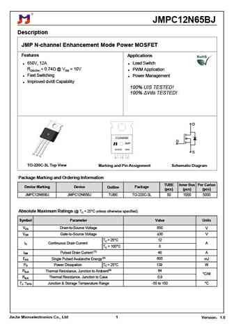
JMPC12N65BJ Description JMP N-channel Enhancement Mode Power MOSFET Features Applications 650V, 12A Load Switch RDS(ON)
lnd12n65 lnc12n65 lne12n65 lnf12n65 lndn12n65.pdf
LND12N65/LNC12N65/LNE12N65/LNF12N65/LNDN12N65 Lonten N-channel 650V, 12A Power MOSFET Description Product Summary The Power MOSFET is fabricated using the V 650V DSS advanced planer VDMOS technology. The I 12A D resulting device has low conduction resistance, R 0.8 DS(on),max superior switching performance and high avalanche Q 41.9 nC g,typ energy. Features Low R DS(on)
lnd12n65 lnc12n65 lne12n65 lnf12n65.pdf
LND12N65/LNC12N65/LNE12N65/LNF12N65 Lonten N-channel 650V, 12A Power MOSFET Description Product Summary The Power MOSFET is fabricated using the VDSS 650V advanced planer VDMOS technology. The ID 12A resulting device has low conduction resistance, RDS(on),max 0.8 superior switching performance and high avalanche Qg,typ 41.9 nC energy. Features Low RDS(on) Low gate
f12n65.pdf
Jingdao Microelectronics co.LTD F12N65 ITO-220ABW 12A, 650V N-CHANNEL POWER MOSFET DESCRIPTION The F12N65 is a high voltage power MOSFET combines advanced trench MOSFET designed to have better characteristics, such as fast switching time, low gate charge, low on-state resistance and high rugged avalanche characteristics. This pow
ptf12n65.pdf
PTF1 2N65 65 0V/1 2A N-Channel A dv anced Power MOSFET Features RDS(on) (Typical 0.5 )@VGS=10V Improved dv/dt Capability, High Ruggedness 100% Avalanche Tested Maximum Junction Temperature Range (150 C) G D S TO-220F Absolute Maximum Ratings Stresses exceeding Maximum Ratings may damage the device. Maximum Ratings are stress ratings only. Functional operation above
se12n65.pdf
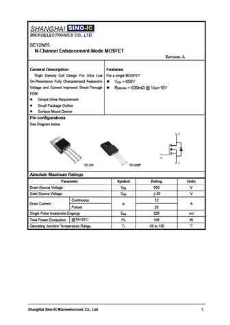
SE12N65 N-Channel Enhancement-Mode MOSFET Revision A General Description Features Thigh Density Cell Design For Ultra Low For a single MOSFET On-Resistance Fully Characterized Avalanche V =650V DS Voltage and Current Improved Shoot-Through R =630m @V =10V DS(ON) GS FOM Simple Drive Requirement Small Package Outline Surface Mount Device Pin configurations
smirf12n65.pdf
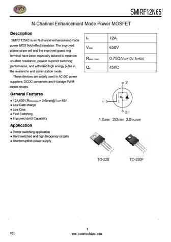
SMIRF12N65 30V /36A Single N Power MOSFET N-Channel Enhancement Mode Power MOSFET Description ID 12A SMIRF12N65 is an N-channel enhancement mode power MOS field effect transistor. The improved VDSS 650V planar stripe cell and the improved guard ring terminal have been especially tailored to minimize Rdson max 0.75 (VGS=10V, ID=6A) on-state resistance, provide superior
vbzmb12n65.pdf
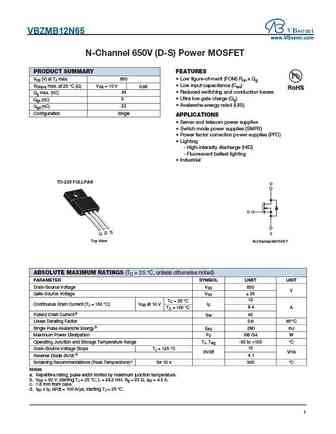
VBZMB12N65 www.VBsemi.com N-Channel 650V (D-S) Power MOSFET FEATURES PRODUCT SUMMARY VDS (V) at TJ max. 650 Low figure-of-merit (FOM) Ron x Qg Low input capacitance (Ciss) RDS(on) max. at 25 C ( ) VGS = 10 V 0.68 43 Reduced switching and conduction losses Qg max. (nC) Ultra low gate charge (Qg) 5 Qgs (nC) Avalanche energy rated (UIS) 22 Qgd (nC) Configu
hm12n65 hm12n65f.pdf
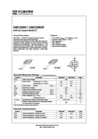
HM12N65 / HM12N65F 650V N-Channel MOSFET General Description Features This Power MOSFET is produced using SL semi s 12.0A, 650V, RDS(on) = 0.75 @VGS = 10 V advanced planar stripe DMOS technology. Low gate charge ( typical 52nC) This advanced technology has been espe cially tailored to High ruggedness minimize o n-state r esistance, pr ovide superior switching Fast w
mpf12n65.pdf
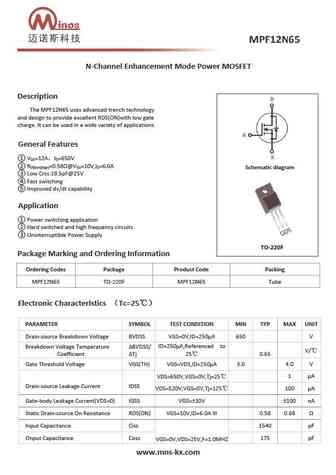
N-Channel Enhancement Mode Power MOSFET Description The MPF12N65 uses advanced trench technology and design to provide excellent RDS(ON)with low gate charge. It can be used in a wide variety of applications. General Features V =12A I =650V DS D R =0.58 @V =10V,I =6.0A DS(on)(typ) GS D Schematic diagram Low Crss 18.5pF@25V Fast switching Improved dv/dt capabil
fxn12n65f.pdf
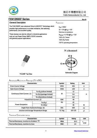
FuXin Semiconductor Co., Ltd. FXN12N65F Series Rev.A General Description Features The FXN12N65F uses advanced Silicon s MOSFET Technology, which V = 650V DS provides high performance in on-state resistance, fast switching ID = 12A @V = 10V GS performance, and excellent quality. Very low on-resistance These devices can also be utilized in ind
mpva12n65f.pdf
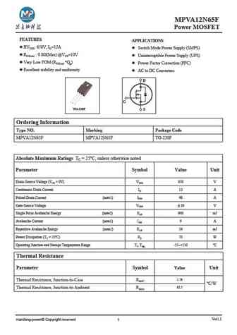
MPVA12N65F Power MOSFET MPSW60M041 FEATURES APPLICATIONS l BVDSS 650V, ID=12A l Switch Mode Power Supply (SMPS) l RDS(on) 0.8 (Max) @VGS=10V l Uninterruptible Power Supply (UPS) l Very Low FOM (RDS(on) *Qg) l Power Factor Correction (PFC) l Excellent stability and uniformity l AC to DC Converters D G TO-220F S Ordering Information Type NO. Marking Package Code MPVA12N6
h12n65p h12n65f.pdf
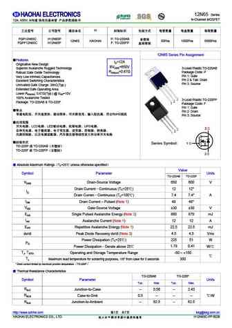
12N65 Series N-Channel MOSFET 12A, 650V, N H FQP12N65C H12N65P P TO-220AB 12N65 HAOHAI 50Pcs 1000Pcs 5000Pcs FQPF12N65C H12N65F F TO-220FP 12N65 Series Pin Assignment Features ID=12A Originative New Des
aob12n65l.pdf

isc N-Channel MOSFET Transistor AOB12N65L FEATURES Drain Current I =12A@ T =25 D C Drain Source Voltage- V =650V(Min) DSS Static Drain-Source On-Resistance R = 0.72 (Max) DS(on) 100% avalanche tested Minimum Lot-to-Lot variations for robust device performance and reliable operation DESCRIPTION Designed for use in switch mode power supplies and general purpo
aotf12n65.pdf
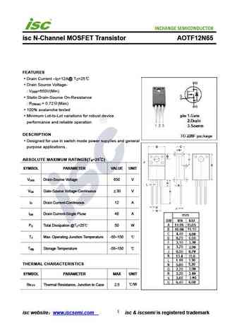
isc N-Channel MOSFET Transistor AOTF12N65 FEATURES Drain Current I =12A@ T =25 D C Drain Source Voltage- V =650V(Min) DSS Static Drain-Source On-Resistance R = 0.72 (Max) DS(on) 100% avalanche tested Minimum Lot-to-Lot variations for robust device performance and reliable operation DESCRIPTION Designed for use in switch mode power supplies and general purpo
ixfp12n65x2m.pdf
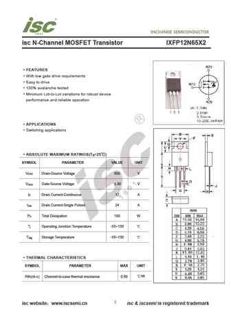
INCHANGE Semiconductor isc N-Channel MOSFET Transistor IXFP12N65X2M FEATURES With low gate drive requirements Easy to drive 100% avalanche tested Minimum Lot-to-Lot variations for robust device performance and reliable operation APPLICATIONS Switching applications ABSOLUTE MAXIMUM RATINGS(T =25 ) a SYMBOL PARAMETER VALUE UNIT V Drain-Source Voltage 650 V DSS V G
aob12n65.pdf
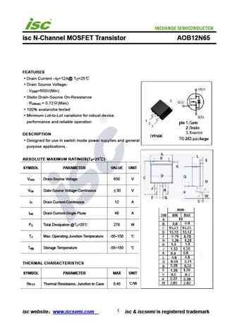
isc N-Channel MOSFET Transistor AOB12N65 FEATURES Drain Current I =12A@ T =25 D C Drain Source Voltage- V =650V(Min) DSS Static Drain-Source On-Resistance R = 0.72 (Max) DS(on) 100% avalanche tested Minimum Lot-to-Lot variations for robust device performance and reliable operation DESCRIPTION Designed for use in switch mode power supplies and general purpos
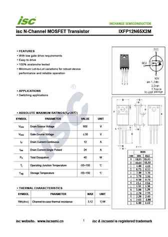
ixfp12n65x2.pdf
isc N-Channel MOSFET Transistor IXFP12N65X2 FEATURES With low gate drive requirements Easy to drive 100% avalanche tested Minimum Lot-to-Lot variations for robust device performance and reliable operation APPLICATIONS Switching applications ABSOLUTE MAXIMUM RATINGS(T =25 ) a SYMBOL PARAMETER VALUE UNIT V Drain-Source Voltage 650 V DSS V Gate-Source Voltage 30 V
12n65kl-tf1-t.pdf
isc N-Channel MOSFET Transistor 12N65KL-TF1-T FEATURES Static Drain-Source On-Resistance R
aow12n65.pdf
isc N-Channel MOSFET Transistor AOW12N65 FEATURES Drain Current I =12A@ T =25 D C Drain Source Voltage- V =650V(Min) DSS Static Drain-Source On-Resistance R = 0.72 (Max) DS(on) 100% avalanche tested Minimum Lot-to-Lot variations for robust device performance and reliable operation DESCRIPTION Designed for use in switch mode power supplies and general purpos
aot12n65.pdf
isc N-Channel MOSFET Transistor AOT12N65 FEATURES Drain Current I =12A@ T =25 D C Drain Source Voltage- V =650V(Min) DSS Static Drain-Source On-Resistance R = 0.72 (Max) DS(on) 100% avalanche tested Minimum Lot-to-Lot variations for robust device performance and reliable operation DESCRIPTION Designed for use in switch mode power supplies and general purpos
aotf12n65l.pdf
isc N-Channel MOSFET Transistor AOTF12N65L FEATURES Drain Current I =12A@ T =25 D C Drain Source Voltage- V =650V(Min) DSS Static Drain-Source On-Resistance R = 0.72 (Max) DS(on) 100% avalanche tested Minimum Lot-to-Lot variations for robust device performance and reliable operation DESCRIPTION Designed for use in switch mode power supplies and general purp
12n65tf.pdf
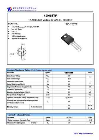
12N65TF 12 Amps,650 Volts N-CHANNEL MOSFET FEATURE TO-220TF 12A,650V,R =0.75 @V =10V/6A DS(ON)MAX GS Low gate charge Low C iss Fast switching 100% avalanche tested Improved dv/dt capability Absolute Maximum Ratings(T =25 ,unless otherwise noted) C Parameter Symbol UNIT 12N65TF Drain-Source Voltage V 650 DSS V Gate-Source Voltage V 30 GSS Continu
ap12n65f ap12n65p.pdf

AP12N65FIP 650V N-Channel Enhancement Mode MOSFET Description The AP12N65F/P is silicon N-channel Enhanced VDMOSFETs, is obtained by the self-aligned planar Technology which reduce the conduction loss, improve switching performance and enhance the avalanche energy. The transistor can be used in various power switching circuit for system miniaturization and higher efficiency.
Другие MOSFET... 10N50TF , 11N65GS , 11N65TFS , 12N60B , 12N60H , 12N65 , 12N65F , 12N65B , 7N60 , 12N65TF , 13N50MF , 150N06Y , 16N65MF , 18N50MF , 20N65NF , 25N06G , 47N60YS .
🌐 : EN ES РУ

Список транзисторов
Обновления
MOSFET: ASA60R150E | ASA60R090EFDA | ASA60R090EFD | ASA50R130E | ADW120N080G2 | ADQ120N080G2 | ADG120N080G2 | AS6004 | 2N7002EY | AS2310A | 2N7002KM | 2N7002KH | AON5802 | AOSS62934 | AOSN21319C | AONS66966
Popular searches
a1693 datasheet | bdw94c equivalent | c2389 | c495 transistor | c5242 reemplazo | d667 transistor datasheet | hy1d datasheet | mp20a transistor