DMP4065SQ. Аналоги и основные параметры
Наименование производителя: DMP4065SQ
Тип транзистора: MOSFET
Полярность: P
Предельные значения
Pd ⓘ
- Максимальная рассеиваемая мощность: 1.4 W
|Vds|ⓘ - Максимально допустимое напряжение сток-исток: 40 V
|Vgs|ⓘ - Максимально допустимое напряжение затвор-исток: 20 V
|Id| ⓘ - Максимально допустимый постоянный ток стока: 3.4 A
Tj ⓘ - Максимальная температура канала: 150 °C
Электрические характеристики
tr ⓘ -
Время нарастания: 2.9 ns
Cossⓘ - Выходная емкость: 88 pf
RDSonⓘ - Сопротивление сток-исток открытого транзистора: 0.08 Ohm
Тип корпуса: SOT23
Аналог (замена) для DMP4065SQ
- подборⓘ MOSFET транзистора по параметрам
DMP4065SQ даташит
..1. Size:437K diodes
dmp4065sq.pdf 
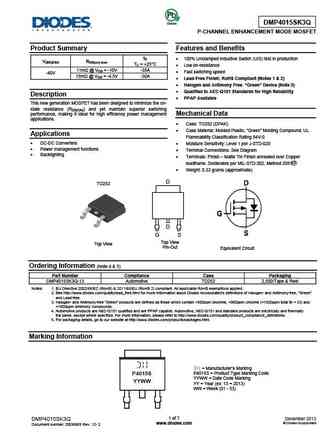
DMP4065SQ 40V P-CHANNEL ENHANCEMENT MODE MOSFET Product Summary Features and Benefits Low On-Resistance ID max BVDSS RDS(ON) max Low Input Capacitance TA = +25 C Fast Switching Speed -3.4A 80m @ VGS = -10V Low Input/Output Leakage -40V Totally Lead-Free & Fully RoHS Compliant (Notes 1 & 2) 100m @ VGS = -4.5V -3.0A Halogen and Antimony F
6.1. Size:470K diodes
dmp4065s.pdf 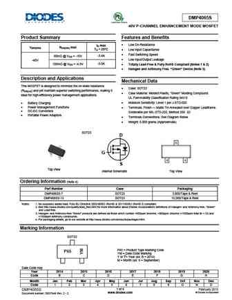
DMP4065S 40V P-CHANNEL ENHANCEMENT MODE MOSFET Product Summary Features and Benefits Low On-Resistance ID max V(BR)DSS RDS(ON) max TA = 25 C Low Input Capacitance Fast Switching Speed -3.4A 80m @ VGS = -10V Low Input/Output Leakage -40V 100m @ VGS = -4.5V -3.0A Totally Lead-Free & Fully RoHS Compliant (Notes 1 & 2) Halogen and Antimon
9.1. Size:359K 1
dmp4015sps-13.pdf 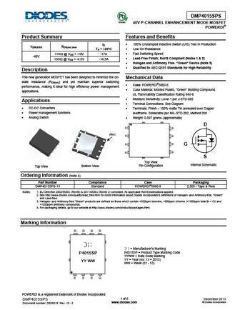
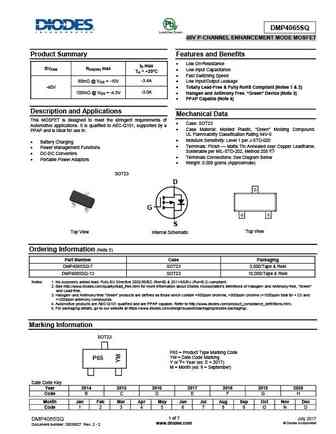
DMP4015SPS Green 40V P-CHANNEL ENHANCEMENT MODE MOSFET POWERDI Product Summary Features and Benefits 100% Unclamped Inductive Switch (UIS) Test In Production ID V(BR)DSS RDS(on) max TA = +25 C Low On-Resistance Fast Switching Speed 11m @ VGS = -10V -17A -40V Lead-Free Finish; RoHS Compliant (Notes 1 & 2) 15m @ VGS = -4.5V -14.5A Halogen and
9.2. Size:363K diodes
dmp4015spsq.pdf 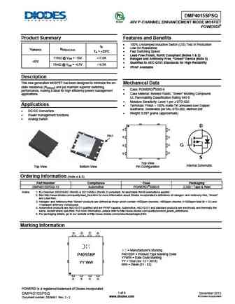
DMP4015SPSQ Green 40V P-CHANNEL ENHANCEMENT MODE MOSFET POWERDI Product Summary Features and Benefits 100% Unclamped Inductive Switch (UIS) Test In Production ID Low On-Resistance V(BR)DSS RDS(on) max TA = +25 C Fast Switching Speed Lead-Free Finish; RoHS Compliant (Notes 1 & 2) 11m @ VGS = -10V -17.0A Halogen and Antimony Free. Green Device
9.3. Size:281K diodes
dmp4047ssd.pdf 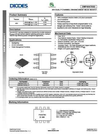
DMP4047SSD 40V DUAL P-CHANNEL ENHANCEMENT MODE MOSFET Product Summary Features 100% Unclamped Inductive Switch (UIS) test in production ID V(BR)DSS RDS(on) Low on-resistance TA = +25 C Fast switching speed 45m @ VGS = -10V -6.5A -40V Totally Lead-Free & Fully RoHS compliant (Note 1 & 2) 55m @ VGS = -4.5V -5.9A Halogen and Antimony Free. Gre
9.4. Size:270K diodes
dmp4015sssq.pdf 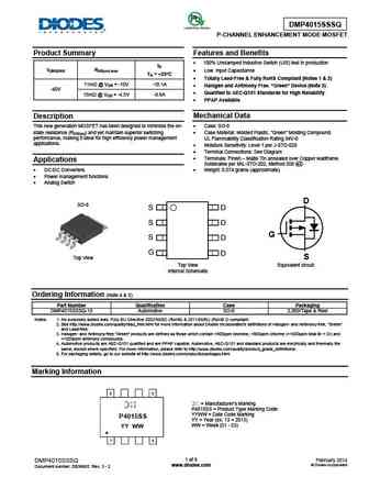
DMP4015SSSQ P-CHANNEL ENHANCEMENT MODE MOSFET Product Summary Features and Benefits 100% Unclamped Inductive Switch (UIS) test in production ID V(BR)DSS RDS(on) max Low Input Capacitance TA = +25 C Totally Lead-Free & Fully RoHS Compliant (Notes 1 & 2) 11m @ VGS = -10V -10.1A Halogen and Antimony Free. Green Device (Note 3) -40V Qualified to
9.5. Size:202K diodes
dmp4015sps.pdf 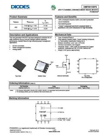
DMP4015SPS Green 40V P-CHANNEL ENHANCEMENT MODE MOSFET POWERDI Product Summary Features and Benefits 100% Unclamped Inductive Switch (UIS) test in production ID V(BR)DSS RDS(on) max Low on-resistance TA = 25 C Fast switching speed 11m @ VGS = -10V -17.0A " Green component and RoHS compliant (Note 1) -40V Qualified to AEC-Q101 Standards for Hig
9.6. Size:286K diodes
dmp4025lsd.pdf 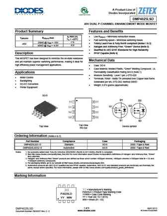
A Product Line of Diodes Incorporated DMP4025LSD 40V DUAL P-CHANNEL ENHANCEMENT MODE MOSFET Product Summary Features and Benefits ID max (A) Low RDS(on) Minimizes conduction losses V(BR)DSS RDS(on) max TA = +25 C Fast switching speed Minimizes switching losses 25m @ VGS = -10V -7.6 Totally Lead-Free & Fully RoHS compliant (Notes 1 & 2) -40V 45m @
9.7. Size:224K diodes
dmp4015sk3.pdf 
DMP4015SK3 P-CHANNEL ENHANCEMENT MODE MOSFET Product Summary Features and Benefits 100% Unclamped Inductive Switch (UIS) test in production ID V(BR)DSS RDS(on) max Low on-resistance TA = 25 C Fast switching speed 11m @ VGS = -10V -14.0A Green component and RoHS compliant (Note 1) -40V Qualified to AEC-Q101 Standards for High Reliability 15m
9.8. Size:236K diodes
dmp4047lfde.pdf 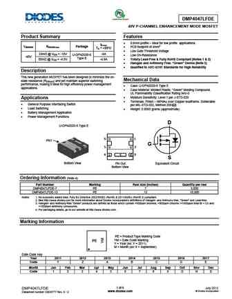
DMP4047LFDE 40V P-CHANNEL ENHANCEMENT MODE MOSFET Product Summary Features 0.6mm profile ideal for low profile applications ID max V(BR)DSS RDS(ON) max Package PCB footprint of 4mm2 TA = +25 C Low Gate Threshold Voltage 33m @ VGS = -10V -6A U-DFN2020-6 Low On-Resistance -40V Type E 50m @ VGS = -4.5V -4.9A Totally Lead-Free & Fully RoHS Com
9.9. Size:263K diodes
dmp4025sfg.pdf 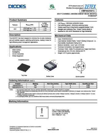
A Product Line of Diodes Incorporated DMP4025SFG 40V P-CHANNEL ENHANCEMENT MODE MOSFET POWERDI Product Summary Features ID max Low RDS(on) Minimizes conduction losses V(BR)DSS RDS(on) max TA = +25 C Fast switching speed Minimizes switching losses (Notes 6) Totally Lead-Free & Fully RoHS compliant (Notes 1 & 2) 25m @ VGS = -10V - 7.2A -40V Hal
9.11. Size:516K diodes
dmp4013lfg.pdf 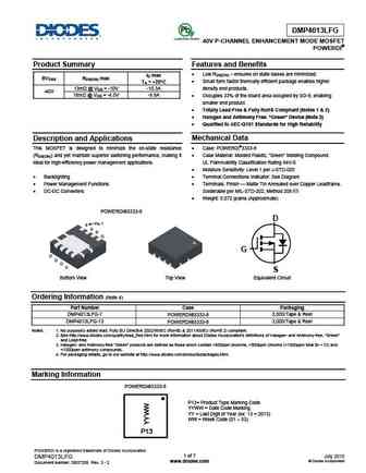
DMP4013LFG 40V P-CHANNEL ENHANCEMENT MODE MOSFET POWERDI Product Summary Features and Benefits Low RDS(ON) ensures on state losses are minimized. ID max BVDSS RDS(ON) max Small form factor thermally efficient package enables higher TA = +25 C 13m @ VGS = -10V -10.3A density end products. -40V 18m @ VGS = -4.5V -8.8A Occupies 33% of the board area
9.12. Size:668K diodes
dmp4051lk3.pdf 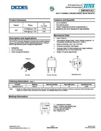
A Product Line of Diodes Incorporated Green DMP4051LK3 40V P-CHANNEL ENHANCEMENT MODE MOSFET Product Summary Features and Benefits Low on-resistance ID V(BR)DSS RDS(on) Fast switching speed TA = 25 C Green component and RoHS compliant (Note 1) 51m @ VGS= -10V -10.5A Qualified to AEC-Q101 Standards for High Reliability -40V 85m @ VGS= -4.5V -8.4
9.13. Size:701K diodes
dmp4050ssd.pdf 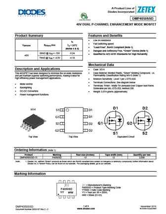
A Product Line of Diodes Incorporated DMP4050SSD 40V DUAL P-CHANNEL ENHANCEMENT MODE MOSFET Product Summary Features and Benefits Low on-resistance ID Fast switching speed V(BR)DSS RDS(on) Max TA = 25 C Lead-Free , RoHS Compliant (Note 1) (Notes 4 & 6) Halogen and Antimony Free, Green Device (Note 1) 50m @ VGS = -10V -5.2A Qualified to
9.14. Size:187K diodes
dmp4025lss.pdf 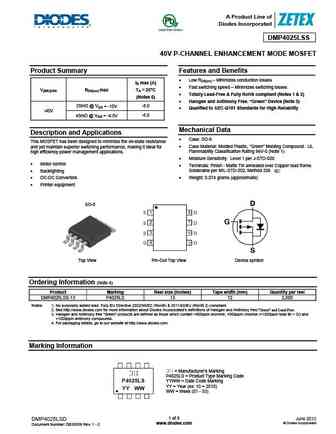
A Product Line of Diodes Incorporated DMP4025LSS 40V P-CHANNEL ENHANCEMENT MODE MOSFET Product Summary Features and Benefits Low RDS(on) Minimizes conduction losses ID max (A) Fast switching speed Minimizes switching losses V(BR)DSS RDS(on) max TA = 25 C Totally Lead-Free & Fully RoHS compliant (Notes 1 & 2) (Notes 6) Halogen and Antimony Free. Gr
9.15. Size:603K diodes
dmp4013lfgq.pdf 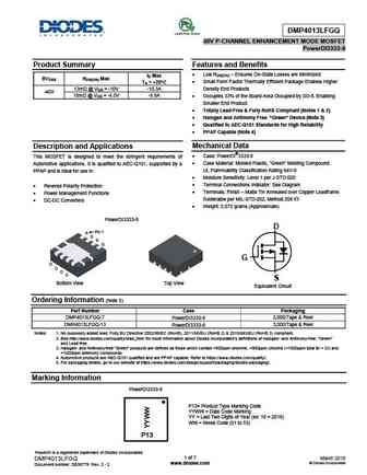
DMP4013LFGQ 40V P-CHANNEL ENHANCEMENT MODE MOSFET PowerDI3333-8 Product Summary Features and Benefits Low RDS(ON) Ensures On-State Losses are Minimized ID Max BVDSS RDS(ON) Max Small Form Factor Thermally Efficient Package Enables Higher TA = +25 C 13m @ VGS = -10V -10.3A Density End Products -40V 18m @ VGS = -4.5V -8.8A Occupies 33% of the Board
9.16. Size:189K diodes
dmp4015sss.pdf 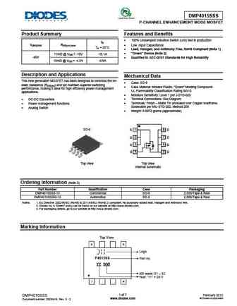
DMP4015SSS P-CHANNEL ENHANCEMENT MODE MOSFET Product Summary Features and Benefits 100% Unclamped Inductive Switch (UIS) test in production ID V(BR)DSS RDS(on) max Low Input Capacitance TA = 25 C Lead, Halogen, and Antimony Free, RoHS Compliant (Note 1) "Green" Device (Note 2) 11m @ VGS = -10V -10.1A -40V Qualified to AEC-Q101 Standards for High Rel
9.17. Size:254K diodes
dmp4025lk3.pdf 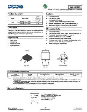
DMP4025LK3 40V P-CHANNEL ENHANCEMENT MODE MOSFET Product Summary Features Low On-Resistance ID max BVDSS RDS(on) max TA = +25 C Fast Switching Speed (Note 6) Low Input/Output Leakage 25m @ VGS = -10V -8.6A Lead-Free Finish; RoHS compliant (Note 1 & 2) -40V 45m @ VGS = -4.5V -7.0A Halogen and Antimony Free. Green Device (Note 3) Quali
9.18. Size:624K diodes
dmp4047sk3.pdf 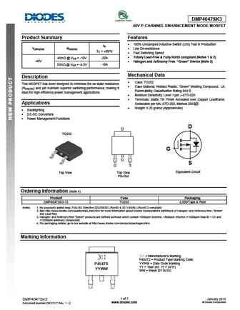
DMP4047SK3 40V P-CHANNEL ENHANCEMENT MODE MOSFET Product Summary Features 100% Unclamped Inductive Switch (UIS) Test in Production ID V(BR)DSS RDS(ON) Low On-resistance TC = +25 C Fast Switching Speed Totally Lead-Free & Fully RoHS compliant (Notes 1 & 2) 45m @ VGS = -10V -20A -40V Halogen and Antimony Free. Green Device (Note 3) 55m @ VG
9.19. Size:671K diodes
dmp4050sss.pdf 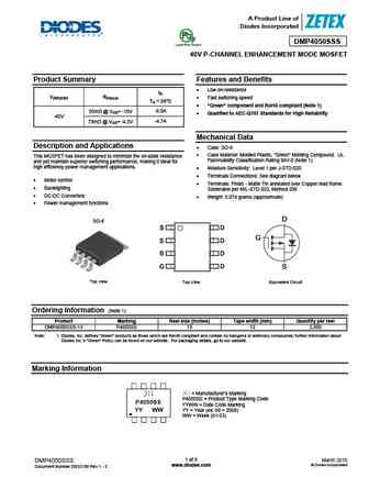
A Product Line of Diodes Incorporated DMP4050SSS 40V P-CHANNEL ENHANCEMENT MODE MOSFET Product Summary Features and Benefits Low on-resistance ID V(BR)DSS RDS(on) Fast switching speed TA = 25 C Green component and RoHS compliant (Note 1) 50m @ VGS= -10V -6.0A Qualified to AEC-Q101 Standards for High Reliability -40V 79m @ VGS= -4.5V -4.7A Me
9.20. Size:1482K cn vbsemi
dmp4015sssq.pdf 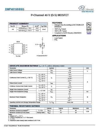
DMP4015SSSQ www.VBsemi.tw P-Channel 40 V (D-S) MOSFET FEATURES PRODUCT SUMMARY Halogen-free According to IEC 61249-2-21 VDS (V) RDS(on) ( )ID (A)a Qg (Typ.) Definition 0.010 at VGS = - 10 V - 16.1 100 % Rg Tested - 40 33 nC 0.014 at VGS = - 4.5 V - 13.3 100 % UIS Tested Compliant to RoHS Directive 2002/95/EC APPLICATIONS S Load Switch POL SO-8 G SD
9.21. Size:850K cn vbsemi
dmp4025lsd.pdf 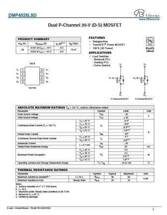
DMP4025LSD www.VBsemi.tw Dual P-Channel 30-V (D-S) MOSFET FEATURES PRODUCT SUMMARY Halogen-free VDS (V) RDS(on) ( ) ID (A)d, e Qg (Typ.) TrenchFET Power MOSFET 0.021 at VGS = - 10 V - 9.5 100 % UIS Tested RoHS - 30 15 nC COMPLIANT 0.028 at VGS = - 4.5 V - 8.0 APPLICATIONS Load Switches - Notebook PCs - Desktop PCs SO-8 S1 S2 - Game Stations S1 1 D1 8
9.22. Size:266K inchange semiconductor
dmp4015sk3.pdf 
isc P-Channel MOSFET Transistor DMP4015SK3 FEATURES Drain Current I = -35A@ T =25 D C Drain Source Voltage- V = -40V(Min) DSS Static Drain-Source On-Resistance R = 11m (Max) DS(on) 100% avalanche tested Minimum Lot-to-Lot variations for robust device performance and reliable operation DESCRIPTION Designed for use in switch mode power supplies and general pu
9.23. Size:266K inchange semiconductor
dmp4051lk3.pdf 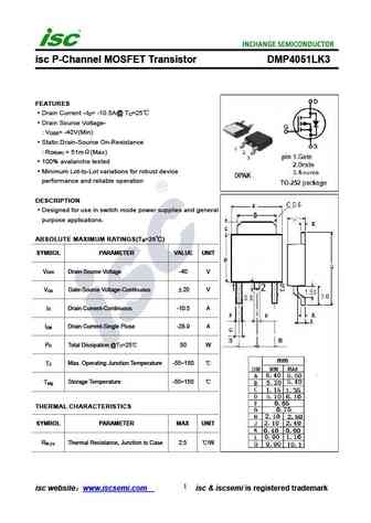
isc P-Channel MOSFET Transistor DMP4051LK3 FEATURES Drain Current I = -10.5A@ T =25 D C Drain Source Voltage- V = -40V(Min) DSS Static Drain-Source On-Resistance R = 51m (Max) DS(on) 100% avalanche tested Minimum Lot-to-Lot variations for robust device performance and reliable operation DESCRIPTION Designed for use in switch mode power supplies and general
9.24. Size:266K inchange semiconductor
dmp4025lk3.pdf 
isc P-Channel MOSFET Transistor DMP4025LK3 FEATURES Drain Current I = -8.6A@ T =25 D C Drain Source Voltage- V = -40V(Min) DSS Static Drain-Source On-Resistance R = 25m (Max) DS(on) 100% avalanche tested Minimum Lot-to-Lot variations for robust device performance and reliable operation DESCRIPTION Designed for use in switch mode power supplies and general p
Другие IGBT... DMP3007SPS, DMP3013SFV, DMP3017SFGQ, DMP3036SFV, DMP3098LQ, DMP3125L, DMP32D5SFB, DMP4013LFGQ, IRFB4115, DMP510DL, DMP6050SFG, DMP610DL, DMP6110SVT, DMP6180SK3Q, DMP6185SEQ, DMP6350S, DMPH6050SK3