DMN60H3D5SK3. Аналоги и основные параметры
Наименование производителя: DMN60H3D5SK3
Тип транзистора: MOSFET
Полярность: N
Предельные значения
Pd ⓘ
- Максимальная рассеиваемая мощность: 41 W
|Vds|ⓘ - Максимально допустимое напряжение сток-исток: 600 V
|Vgs|ⓘ - Максимально допустимое напряжение затвор-исток: 30 V
|Id| ⓘ - Максимально допустимый постоянный ток стока: 2.8 A
Tj ⓘ - Максимальная температура канала: 150 °C
Электрические характеристики
tr ⓘ -
Время нарастания: 22 ns
Cossⓘ - Выходная емкость: 41 pf
RDSonⓘ - Сопротивление сток-исток открытого транзистора: 3.5 Ohm
Тип корпуса: TO252
Аналог (замена) для DMN60H3D5SK3
- подборⓘ MOSFET транзистора по параметрам
DMN60H3D5SK3 даташит
..1. Size:542K diodes
dmn60h3d5sk3.pdf 

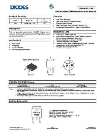
Green DMN60H3D5SK3 600V N-CHANNEL ENHANCEMENT MODE MOSFET Product Summary Features Low Input Capacitance ID BVDSS RDS(ON) Max TC = +25 C High BVDSS Rating for Power Application 600V 3.5 @ VGS = 10V 2.8A Low Input/Output Leakage Lead-Free Finish; RoHS Compliant (Notes 1 & 2) Halogen and Antimony Free. Green Device (Note 3) Description This new
..2. Size:266K inchange semiconductor
dmn60h3d5sk3.pdf 

isc N-Channel MOSFET Transistor DMN60H3D5SK3 FEATURES Drain Current I = 2.8A@ T =25 D C Drain Source Voltage- V = 600V(Min) DSS Static Drain-Source On-Resistance R = 3.5 (Max) DS(on) 100% avalanche tested Minimum Lot-to-Lot variations for robust device performance and reliable operation DESCRIPTION Designed for use in switch mode power supplies and general
8.1. Size:330K diodes
dmn60h4d5sk3.pdf 

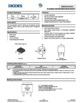
DMN60H4D5SK3 N-CHANNEL ENHANCEMENT MODE MOSFET Product Summary Features Low Input Capacitance ID BVDSS RDS(ON) TC = +25 High BVDSS Rating for Power Application C 600V 4.5 @VGS = 10V 2.5A Low Input/Output Leakage Lead-Free Finish; RoHS Compliant (Notes 1 & 2) Halogen and Antimony Free. Green Device (Note 3) Description This new generation MOSF
8.2. Size:266K inchange semiconductor
dmn60h4d5sk3.pdf 

isc N-Channel MOSFET Transistor DMN60H4D5SK3 FEATURES Drain Current I = 2.5A@ T =25 D C Drain Source Voltage- V = 600V(Min) DSS Static Drain-Source On-Resistance R = 4.5 (Max) DS(on) 100% avalanche tested Minimum Lot-to-Lot variations for robust device performance and reliable operation DESCRIPTION Designed for use in switch mode power supplies and general
9.1. Size:667K diodes
dmn6068lk3.pdf 

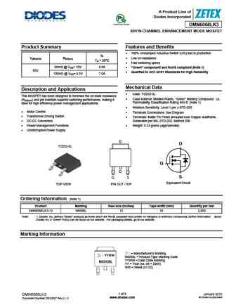
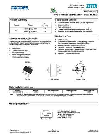
A Product Line of Diodes Incorporated DMN6068LK3 60V N-CHANNEL ENHANCEMENT MODE MOSFET Product Summary Features and Benefits 100% Unclamped Inductive Switch (UIS) test in production ID V(BR)DSS RDS(on) Low on-resistance TA = 25 C Fast switching speed 68m @ VGS= 10V 8.5A Green component and RoHS compliant (Note 1) 60V Qualified to AEC-Q101 Stan
9.2. Size:243K diodes
dmn6040ssd.pdf 

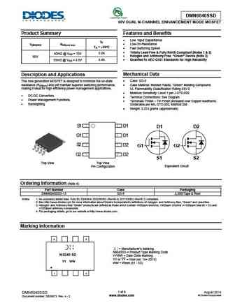
DMN6040SSD 60V DUAL N-CHANNEL ENHANCEMENT MODE MOSFET Product Summary Features and Benefits Low Input Capacitance ID Low On-Resistance V(BR)DSS RDS(on) max TA = +25 C Fast Switching Speed Totally Lead-Free & Fully RoHS Compliant (Notes 1 & 2) 40m @ VGS = 10V 5.0A Halogen and Antimony Free. Green Device (Note 3) 60V 4.4A Qualified to AEC
9.3. Size:148K diodes
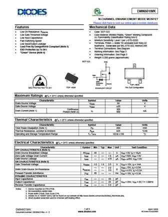
dmn601wk.pdf 

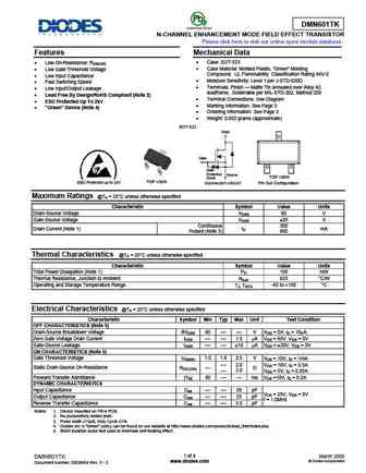
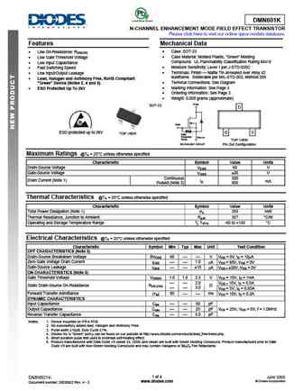
DMN601WK N-CHANNEL ENHANCEMENT MODE MOSFET Please click here to visit our online spice models database. Features Mechanical Data Low On-Resistance RDS(ON) Case SOT-323 Case Material Molded Plastic, Green Molding Compound. Low Gate Threshold Voltage UL Flammability Classification Rating 94V-0 Low Input Capacitance Moisture Sensitivity Level 1 per
9.4. Size:517K diodes
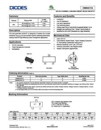
dmn6075s.pdf 

DMN6075S 60V N-CHANNEL ENHANCEMENT MODE MOSFET Summary Features and Benefits ID max N MOSFET V(BR)DSS RDS(ON) max TA = +25 C Low On-Resistance Low Input Capacitance 85 m @ VGS = 10V 2.5A 60V Fast Switching Speed 120 m @ VGS = 4.5V 2.0A Totally Lead-Free & Fully RoHS Compliant (Notes 1 & 2) Halogen and Antimony Free. Green Device (Note
9.5. Size:493K diodes
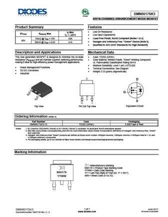
dmn6017sk3.pdf 

DMN6017SK3 Green 60V N-CHANNEL ENHANCEMENT MODE MOSFET Product Summary Features Low On-Resistance ID Max BVDSS RDS(ON) Max Low Input Capacitance TC = +25 C Lead-Free Finish; RoHS Compliant (Notes 1 & 2) 18m @ VGS = 10V 43A 60V Halogen and Antimony Free. Green Device (Note 3) 20m @ VGS = 4.5V 41A Qualified to AEC-Q101 Standards for H
9.6. Size:230K diodes
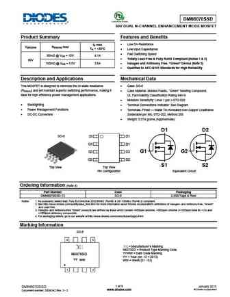
dmn6070ssd.pdf 

DMN6070SSD 60V DUAL N-CHANNEL ENHANCEMENT MODE MOSFET Product Summary Features and Benefits Low On-Resistance ID max V(BR)DSS RDS(ON) max TA = +25 C Low Input Capacitance Fast Switching Speed 80m @ VGS = 10V 4.1A Totally Lead-Free & Fully RoHS Compliant (Notes 1 & 2) 60V 100m @ VGS = 4.5V 3.6A Halogen and Antimony Free. Green Device (Note 3
9.7. Size:322K diodes
dmn6013lfg.pdf 

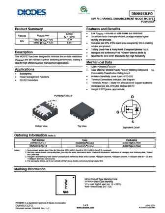
DMN6013LFG 60V N-CHANNEL ENHANCEMENT MODE MOSFET POWERDI Product Summary Features and Benefits Low RDS(ON) ensures on state losses are minimized ID max V(BR)DSS RDS(ON) max Small form factor thermally efficient package enables higher TA = +25 C 13m @ VGS = 10V 10.3A density end products 60V 18m @ VGS = 4.5V 8.8A Occupies just 33% of the board area o
9.8. Size:469K diodes
dmn6040ssdq.pdf 

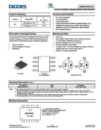
DMN6040SSDQ DUAL N-CHANNEL ENHANCEMENT MODE MOSFET Product Summary Features and Benefits Low Input Capacitance ID V(BR)DSS RDS(ON) Max Low On-Resistance TA = +25 C Fast Switching Speed 40m @ VGS = 10V 5.0A Totally Lead-Free & Fully RoHS Compliant (Notes 1 & 2) 60V Halogen and Antimony Free. Green Device (Note 3) 4.4A 55m @ VGS = 4.5V
9.9. Size:278K diodes
dmn6070sfcl.pdf 

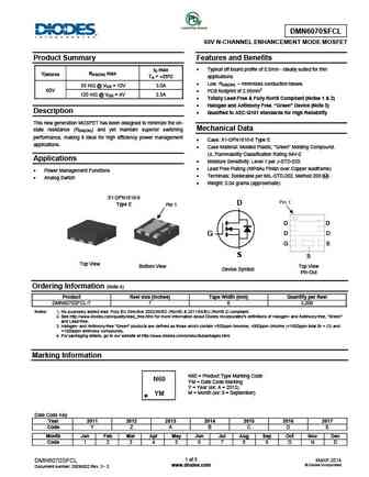
DMN6070SFCL 60V N-CHANNEL ENHANCEMENT MODE MOSFET Product Summary Features and Benefits Typical off board profile of 0.5mm - ideally suited for thin ID max V(BR)DSS RDS(ON) max TA = +25 C applications Low RDS(ON) minimizes conduction losses 85 m @ VGS = 10V 3.0A 60V PCB footprint of 2.56mm2 120 m @ VGS = 4V 2.5A Totally Lead-Free & Fully RoHS C
9.10. Size:706K diodes
dmn6066ssd.pdf 

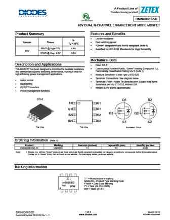
A Product Line of Diodes Incorporated DMN6066SSD 60V DUAL N-CHANNEL ENHANCEMENT MODE MOSFET Product Summary Features and Benefits Low on-resistance ID V(BR)DSS RDS(on) Fast switching speed TA = 25 C Green component and RoHS compliant (Note 1) 66m @ VGS= 10V 4.4A Qualified to AEC-Q101 Standards for High Reliability 60V 97m @ VGS= 4.5V 3.6A Me
9.11. Size:624K diodes
dmn6068se.pdf 

A Product Line of Diodes Incorporated DMN6068SE 60V N-CHANNEL ENHANCEMENT MODE MOSFET Product Summary Features and Benefits 100% Unclamped Inductive Switch (UIS) test in production ID V(BR)DSS RDS(on) Low on-resistance TA = 25 C Fast switching speed 68m @ VGS= 10V 5.6A Green component and RoHS compliant (Note 1) 60V Qualified to AEC-Q101 Stan
9.12. Size:504K diodes
dmn6040svtq.pdf 

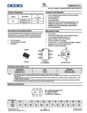
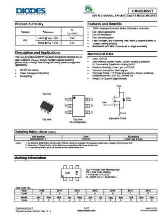
DMN6040SVTQ 60V N-CHANNEL ENHANCEMENT MODE MOSFET Product Summary Features and Benefits 100% Unclamped Inductive Switch (UIS) Test in Production ID V(BR)DSS RDS(ON) Max Low Input Capacitance TA = +25 C Low On-Resistance 44m @ VGS = 10V 5.0A Fast Switching Speed 60V Totally Lead-Free & Fully RoHS Compliant (Notes 1 & 2) 4.3A 60m @ VGS = 4.5V
9.13. Size:198K diodes
dmn601dmk.pdf 

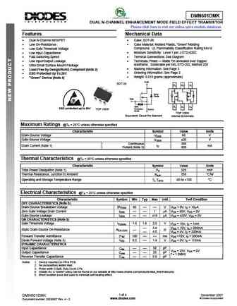
DMN601DMK DUAL N-CHANNEL ENHANCEMENT MODE FIELD EFFECT TRANSISTOR Please click here to visit our online spice models database. Features Mechanical Data Dual N-Channel MOSFET Case SOT-26 Low On-Resistance Case Material Molded Plastic, Green Molding Compound. UL Flammability Classification Rating 94V-0 Low Gate Threshold Voltage Moisture Sensitivity
9.14. Size:238K diodes
dmn6040sk3.pdf 

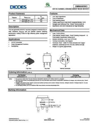
DMN6040SK3 60V N-CHANNEL ENHANCEMENT MODE MOSFET Product Summary Features ID Low Input Capacitance V(BR)DSS RDS(on) max TC = +25 C Low On-Resistance 40m @ VGS = 10V 20A Fast Switching Speed 60V 50m @ VGS = 4.5V 16A Totally Lead-Free & Fully RoHS Compliant (Notes 1 & 2) Halogen and Antimony Free. Green Device (Note 3) Qualified to AEC-Q1
9.15. Size:495K diodes
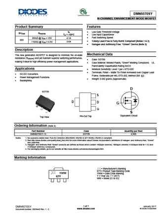
dmn6070sy.pdf 

DMN6070SY N-CHANNEL ENHANCEMENT MODE MOSFET Product Summary Features ID Low Gate Threshold Voltage BVDSS RDS(ON) TA = +25 Low Input Capacitance C Fast Switching Speed 85m @ VGS = 10V 4.1A 60V Totally Lead-Free & Fully RoHS Compliant (Notes 1 & 2) 110m @ VGS = 4.5V 3.6A Halogen and Antimony Free. Green Device (Note 3) Description Me
9.16. Size:195K diodes
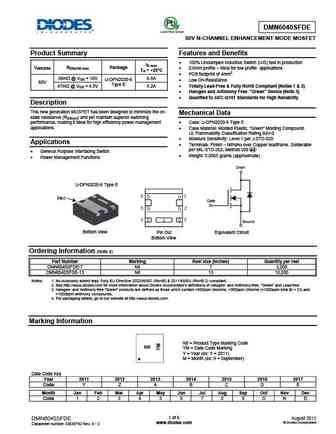
dmn6040sfde.pdf 

DMN6040SFDE 60V N-CHANNEL ENHANCEMENT MODE MOSFET Product Summary Features and Benefits 100% Unclamped Inductive Switch (UIS) test in production ID max V(BR)DSS RDS(ON) max Package 0.6mm profile ideal for low profile applications TA = +25 C PCB footprint of 4mm2 38m @ VGS = 10V 6.5A U-DFN2020-6 Low On-Resistance 60V Type E 47m @ VGS = 4.5V 5.
9.17. Size:172K diodes
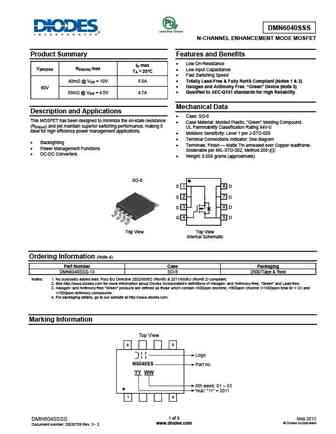
dmn6040sss.pdf 

DMN6040SSS N-CHANNEL ENHANCEMENT MODE MOSFET Product Summary Features and Benefits Low On-Resistance ID max V(BR)DSS RDS(ON) max Low Input Capacitance TA = 25 C Fast Switching Speed 40m @ VGS = 10V 5.5A Totally Lead-Free & Fully RoHS Compliant (Notes 1 & 2) Halogen and Antimony Free. Green Device (Note 3) 60V Qualified to AEC-Q101 standard
9.18. Size:317K diodes
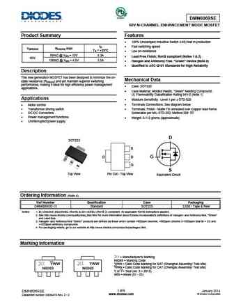
dmn6069se.pdf 

DMN6069SE 60V N-CHANNEL ENHANCEMENT MODE MOSFET Product Summary Features 100% Unclamped Inductive Switch (UIS) test in production ID Fast switching speed V(BR)DSS RDS(ON) max TA = +25 C Low on-resistance 69m @ VGS = 10V 4.3A Lead-Free Finish; RoHS compliant (Notes 1 & 2) 60V 100m @ VGS = 4.5V 3.5A Halogen and Antimony Free. Green Device (
9.19. Size:286K diodes
dmn601vk.pdf 

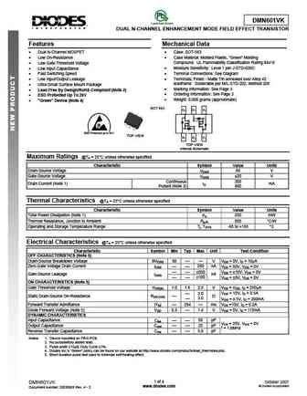
DMN601VK DUAL N-CHANNEL ENHANCEMENT MODE FIELD EFFECT TRANSISTOR Features Mechanical Data Dual N-Channel MOSFET Case SOT-563 Low On-Resistance Case Material Molded Plastic, Green Molding Compound. UL Flammability Classification Rating 94V-0 Low Gate Threshold Voltage Moisture Sensitivity Level 1 per J-STD-020C Low Input Capacitance Termi
9.20. Size:136K diodes
dmn601tk.pdf 

DMN601TK N-CHANNEL ENHANCEMENT MODE FIELD EFFECT TRANSISTOR Please click here to visit our online spice models database. Features Mechanical Data Low On-Resistance RDS(ON) Case SOT-523 Case Material Molded Plastic, Green Molding Low Gate Threshold Voltage Compound. UL Flammability Classification Rating 94V-0 Low Input Capacitance Moisture Sensiti
9.21. Size:678K diodes
dmn6066sss.pdf 

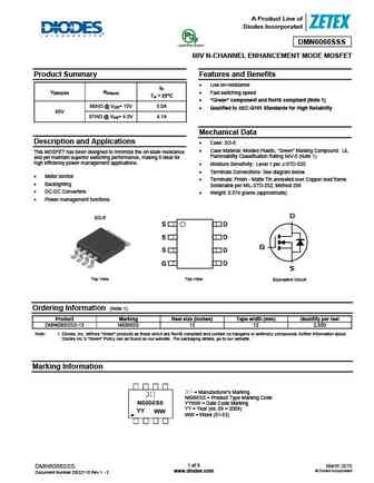
A Product Line of Diodes Incorporated DMN6066SSS 60V N-CHANNEL ENHANCEMENT MODE MOSFET Product Summary Features and Benefits Low on-resistance ID V(BR)DSS RDS(on) Fast switching speed TA = 25 C Green component and RoHS compliant (Note 1) 66m @ VGS= 10V 5.0A Qualified to AEC-Q101 Standards for High Reliability 60V 97m @ VGS= 4.5V 4.1A Mechani
9.22. Size:196K diodes
dmn601dwk.pdf 

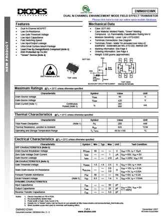
DMN601DWK DUAL N-CHANNEL ENHANCEMENT MODE FIELD EFFECT TRANSISTOR Please click here to visit our online spice models database. Features Mechanical Data Dual N-Channel MOSFET Case SOT-363 Low On-Resistance Case Material Molded Plastic, Green Molding Compound. UL Flammability Classification Rating 94V-0 Low Gate Threshold Voltage Moisture Sensitivity
9.23. Size:185K diodes
dmn601k.pdf 

DMN601K N-CHANNEL ENHANCEMENT MODE FIELD EFFECT TRANSISTOR Please click here to visit our online spice models database. Features Mechanical Data Low On-Resistance RDS(ON) Case SOT-23 Case Material Molded Plastic, Green Molding Low Gate Threshold Voltage Compound. UL Flammability Classification Rating 94V-0 Low Input Capacitance Moisture Sensitivi
9.25. Size:885K cn vbsemi
dmn6068se-13.pdf 

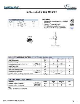
DMN6068SE-13 www.VBsemi.tw N-Channel 60-V (D-S) MOSFET FEATURES PRODUCT SUMMARY Halogen-free According to IEC 61249-2-21 VDS (V) RDS(on) ( )ID (A) Definition 0.029 at VGS = 10 V 7.0 TrenchFET Power MOSFETs 60 0.033 at VGS = 4.5 V 5.6 175 C Maximum Junction Temperature Compliant to RoHS Directive 2002/95/EC D SOT-223 D G S D G S N-Channel MOSF
9.26. Size:1549K cn vbsemi
dmn6070ssd.pdf 

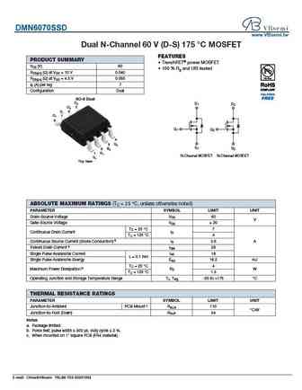
DMN6070SSD www.VBsemi.tw Dual N-Channel 60 V (D-S) 175 C MOSFET FEATURES PRODUCT SUMMARY TrenchFET power MOSFET VDS (V) 60 100 % Rg and UIS tested RDS(on) ( ) at VGS = 10 V 0.040 RDS(on) ( ) at VGS = 4.5 V 0.055 ID (A) per leg 7 Configuration Dual SO-8 Dual D2 D1 D2 D2 5 D1 6 D1 7 8 G1 G2 4 G2 3 3 S1 S2 S2 S2 2 2 G G1 1 1 N-Channel MOSFET N-Chann
9.27. Size:808K cn vbsemi
dmn6040sk3-13.pdf 

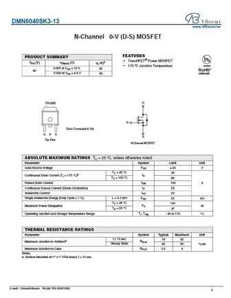
DMN6040SK3-13 www.VBsemi.tw N-Channel 6 0-V (D-S) MOSFET FEATURES PRODUCT SUMMARY TrenchFET Power MOSFET VDS (V) rDS(on) ( ) ID (A)a Available 175 C Junction Temperature 0.025 at VGS = 10 V 35 RoHS* 60 0.030 at VGS = 4.5 V 30 COMPLIANT TO-252 D G Drain Connected to Tab G D S S Top View N-Channel MOSFET ABSOLUTE MAXIMUM RATINGS TC = 25 C, unless otherwi
9.28. Size:892K cn vbsemi
dmn6068lk3-13.pdf 

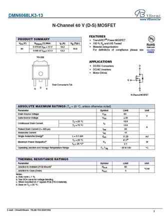
DMN6068LK3-13 www.VBsemi.tw N-Channel 60 V (D-S) MOSFET FEATURES PRODUCT SUMMARY TrenchFET Power MOSFET VDS (V) RDS(on) ( ) Max. ID (A) Qg (Typ.) 100 % Rg and UIS Tested 0.073 at VGS = 10 V 18.2 Material categorization 60 19.8 For definitions of compliance please see 0.085 at VGS = 4.5 V 13.2 TO-252 APPLICATIONS D DC/DC Converters DC/AC Inverters
9.29. Size:266K inchange semiconductor
dmn6068lk3.pdf 

isc N-Channel MOSFET Transistor DMN6068LK3 FEATURES Drain Current I = 8.5A@ T =25 D C Drain Source Voltage- V = 60V(Min) DSS Static Drain-Source On-Resistance R = 68m (Max) DS(on) 100% avalanche tested Minimum Lot-to-Lot variations for robust device performance and reliable operation DESCRIPTION Designed for use in switch mode power supplies and general pur
9.30. Size:266K inchange semiconductor
dmn6017sk3.pdf 
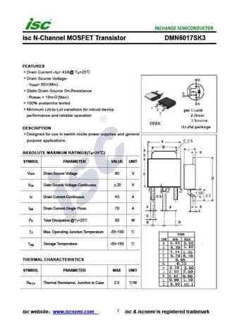
isc N-Channel MOSFET Transistor DMN6017SK3 FEATURES Drain Current I = 43A@ T =25 D C Drain Source Voltage- V = 60V(Min) DSS Static Drain-Source On-Resistance R = 18m (Max) DS(on) 100% avalanche tested Minimum Lot-to-Lot variations for robust device performance and reliable operation DESCRIPTION Designed for use in switch mode power supplies and general purp
9.31. Size:265K inchange semiconductor
dmn6040sk3.pdf 

isc N-Channel MOSFET Transistor DMN6040SK3 FEATURES Drain Current I = 20A@ T =25 D C Drain Source Voltage- V = 60V(Min) DSS Static Drain-Source On-Resistance R = 40m (Max) DS(on) 100% avalanche tested Minimum Lot-to-Lot variations for robust device performance and reliable operation DESCRIPTION Designed for use in switch mode power supplies and general purp
Другие MOSFET... DMJ70H1D4SV3
, DMJ70H1D5SV3
, DMJ70H600SH3
, DMJ70H601SK3
, DMJ70H601SV3
, DMJ70H900HJ3
, DMN15H310SK3
, DMN6017SK3
, IRFP064N
, DMN60H4D5SK3
, DMN80H2D0SCTI
, DMN90H2D2HCTI
, DMN90H8D5HCT
, DMN90H8D5HCTI
, DMN95H2D2HCTI
, DMN95H8D5HCTI
, DMNH10H028SCT
.
History: CM7N60
| SMK830FZ
