2N7000TA datasheet, аналоги, основные параметры
Наименование производителя: 2N7000TA 📄📄
Тип транзистора: MOSFET
Полярность: N
Предельные значения
Pd ⓘ - Максимальная рассеиваемая мощность: 0.4 W
|Vds|ⓘ - Максимально допустимое напряжение сток-исток: 60 V
|Vgs|ⓘ - Максимально допустимое напряжение затвор-исток: 30 V
|Id| ⓘ - Максимально допустимый постоянный ток стока: 0.2 A
Tj ⓘ - Максимальная температура канала: 150 °C
Электрические характеристики
tr ⓘ - Время нарастания: 10 ns
Cossⓘ - Выходная емкость: 12 pf
RDSonⓘ - Сопротивление сток-исток открытого транзистора: 5 Ohm
Тип корпуса: TO92
📄📄 Копировать
Аналог (замена) для 2N7000TA
- подборⓘ MOSFET транзистора по параметрам
2N7000TA даташит
..1. Size:84K fairchild semi
2n7000ta.pdf 
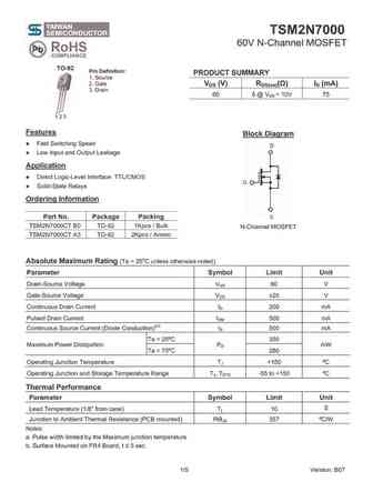
Advanced Small Signal MOSFET 2N7000BU/2N7000TA FEATURES BVDSS = 60 V n Fast Switching Times RDS(on) = 5.0 n Improved Inductive Ruggedness n Lower Input Capacitance ID = 200 mA n Extended Safe Operating Area n Improved High Temperature Reliability TO-92 1.Source 2. Gate 3. Drain Absolute Maximum Ratings Symbol Characteristic Value Units VDSS Drain-to-Source Voltage V 60 Contin
8.2. Size:77K motorola
2n7000r3.pdf 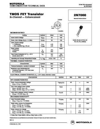
MOTOROLA Order this document SEMICONDUCTOR TECHNICAL DATA by 2N7000/D TMOS FET Transistor 2N7000 N Channel Enhancement Motorola Preferred Device 3 DRAIN 2 GATE 1 SOURCE MAXIMUM RATINGS 1 Rating Symbol Value Unit 2 3 Drain Source Voltage VDSS 60 Vdc CASE 29 04, STYLE 22 Drain Gate Voltage (RGS = 1.0 M ) VDGR 60 Vdc TO 92 (TO 226AA) Gate Source Voltage
8.3. Size:274K philips
2n7000-03.pdf 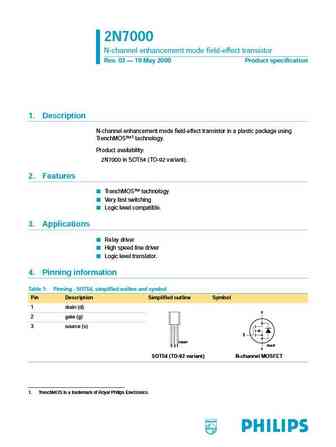
2N7000 N-channel enhancement mode field-effect transistor Rev. 03 19 May 2000 Product specification 1. Description N-channel enhancement mode field-effect transistor in a plastic package using TrenchMOS 1 technology. Product availability 2N7000 in SOT54 (TO-92 variant). 2. Features TrenchMOS technology Very fast switching Logic level compatible. 3. Applications Relay
8.4. Size:626K st
2n7000 2n7002.pdf 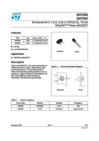
2N7000 2N7002 N-channel 60 V, 1.8 , 0.35 A, SOT23-3L, TO-92 STripFET Power MOSFET Features Type VDSS RDS(on) max ID 3 2N7000 60 V
8.5. Size:109K fairchild semi
2n7000 2n7002 nds7002a.pdf 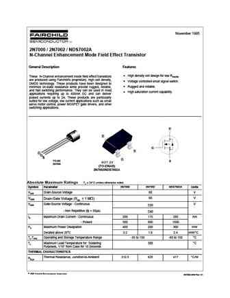
November 1995 2N7000 / 2N7002 / NDS7002A N-Channel Enhancement Mode Field Effect Transistor General Description Features High density cell design for low RDS(ON). These N-Channel enhancement mode field effect transistors are produced using Fairchild's proprietary, high cell density, Voltage controlled small signal switch. DMOS technology. These products have been designed to Rugged
8.6. Size:94K fairchild semi
2n7000.pdf 
November 1995 2N7000 / 2N7002 / NDS7002A N-Channel Enhancement Mode Field Effect Transistor General Description Features High density cell design for low RDS(ON). These N-Channel enhancement mode field effect transistors are produced using Fairchild's proprietary, high cell density, Voltage controlled small signal switch. DMOS technology. These products have been designed to Rugged
8.7. Size:85K fairchild semi
2n7000bu.pdf 
Advanced Small Signal MOSFET 2N7000BU/2N7000TA FEATURES BVDSS = 60 V n Fast Switching Times RDS(on) = 5.0 n Improved Inductive Ruggedness n Lower Input Capacitance ID = 200 mA n Extended Safe Operating Area n Improved High Temperature Reliability TO-92 1.Source 2. Gate 3. Drain Absolute Maximum Ratings Symbol Characteristic Value Units VDSS Drain-to-Source Voltage V 60 Contin
8.8. Size:443K samsung
2n7000.pdf 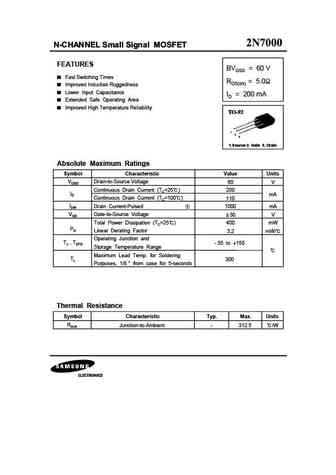
N-CHANNEL SmaII SignaI MOSFET FEATURES BVDSS = 60 V Fast Switching Times RDS(on) = 5.0 Improved Inductive Ruggedness Lower Input Capacitance ID = 200 mA Extended Safe Operating Area Improved High Temperature Reliability TO-92 1 2 3 1.Source 2. Gate 3. Drain Absolute Maximum Ratings Symbol Characteristic Value Units VDSS Drain-to-Source Voltage V 60 Continuous Drain Cur
8.9. Size:93K vishay
2n7000kl bs170kl.pdf 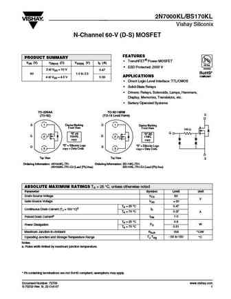
2N7000KL/BS170KL Vishay Siliconix N-Channel 60-V (D-S) MOSFET FEATURES PRODUCT SUMMARY TrenchFET Power MOSFET VDS (V) rDS(on) ( ) VGS(th) (V) ID (A) Pb-free ESD Protected 2000 V Available 2 at VGS = 10 V 0.47 60 1.0 to 2.5 RoHS* APPLICATIONS COMPLIANT 4 at VGS = 4.5 V 0.33 Direct Logic-Level Interface TTL/CMOS Solid-State Relays Drivers Relays,
8.10. Size:58K vishay
2n7000 2n7002 vq1000j-p bs170.pdf 
2N7000/2N7002, VQ1000J/P, BS170 Vishay Siliconix N-Channel 60-V (D-S) MOSFET PRODUCT SUMMARY Part Number V(BR)DSS Min (V) rDS(on) Max (W) VGS(th) (V) ID (A) 5 @ VGS = 10 V 0.8 to 3 0.2 2N7000 2N7002 7.5 @ VGS = 10 V 1 to 2.5 0.115 60 VQ1000J 5.5 @ VGS = 10 V 0.8 to 2.5 0.225 VQ1000P 5.5 @ VGS = 10 V 0.8 to 2.5 0.225 BS170 5 @ VGS = 10 V 0.8 to 3 0.5 FEATURES BENEFITS APPLICATIONS D
8.11. Size:58K vishay
2n7000 2n7002 vq1000j vq1000p bs170.pdf 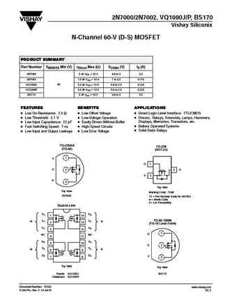
2N7000/2N7002, VQ1000J/P, BS170 Vishay Siliconix N-Channel 60-V (D-S) MOSFET PRODUCT SUMMARY Part Number V(BR)DSS Min (V) rDS(on) Max (W) VGS(th) (V) ID (A) 5 @ VGS = 10 V 0.8 to 3 0.2 2N7000 2N7002 7.5 @ VGS = 10 V 1 to 2.5 0.115 60 VQ1000J 5.5 @ VGS = 10 V 0.8 to 2.5 0.225 VQ1000P 5.5 @ VGS = 10 V 0.8 to 2.5 0.225 BS170 5 @ VGS = 10 V 0.8 to 3 0.5 FEATURES BENEFITS APPLICATIONS D
8.12. Size:736K onsemi
2n7000 2n7002 nds7002a.pdf 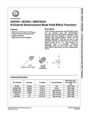
2N7000 / 2N7002 / NDS7002A N-Channel Enhancement Mode Field Effect Transistor Description Features These N-channel enhancement mode field effect transis- High Density Cell Design for Low RDS(ON) tors are produced using ON Semiconductor's Voltage Controlled Small Signal Switch proprietary, high cell density, DMOS technology. These Rugged and Reliable products have been de
8.13. Size:88K onsemi
2n7000g 2n7000rlra 2n7000rlrag 2n7000rlrmg 2n7000rlrpg.pdf 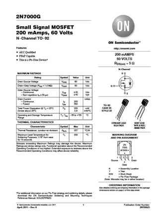
2N7000G Small Signal MOSFET 200 mAmps, 60 Volts N-Channel TO-92 Features http //onsemi.com AEC Qualified 200 mAMPS PPAP Capable 60 VOLTS This is a Pb-Free Device* RDS(on) = 5 W N-Channel MAXIMUM RATINGS D Rating Symbol Value Unit Drain Source Voltage VDSS 60 Vdc Drain-Gate Voltage (RGS = 1.0 MW) VDGR 60 Vdc G Gate-Source Voltage - Continuous VGS 20 Vdc S - No
8.14. Size:92K onsemi
2n7000g.pdf 
2N7000G Small Signal MOSFET 200 mAmps, 60 Volts N-Channel TO-92 Features http //onsemi.com AEC Qualified 200 mAMPS PPAP Capable 60 VOLTS This is a Pb-Free Device* RDS(on) = 5 W N-Channel MAXIMUM RATINGS D Rating Symbol Value Unit Drain Source Voltage VDSS 60 Vdc Drain-Gate Voltage (RGS = 1.0 MW) VDGR 60 Vdc G Gate-Source Voltage - Continuous VGS 20 Vdc S - No
8.15. Size:150K utc
2n7000z.pdf 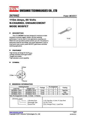
UNISONIC TECHNOLOGIES CO., LTD 2N7000Z Power MOSFET 115m Amps, 60 Volts N-CHANNEL ENHANCEMENT MODE MOSFET DESCRIPTION 1 The UTC 2N7000Z has been designed to minimize on-state resistance to provide rugged, reliable, and fast switching TO-92 performance. It can be used in most applications requiring up to 400mA DC and can deliver pulsed currents up to 2A. The product is p
8.16. Size:355K utc
2n7000.pdf 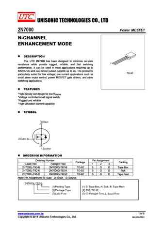
UNISONIC TECHNOLOGIES CO., LTD 2N7000 Power MOSFET N-CHANNEL ENHANCEMENT MODE DESCRIPTION The UTC 2N7000 has been designed to minimize on-state 1 resistance while provide rugged, reliable, and fast switching performance. It can be used in most applications requiring up to 400mA DC and can deliver pulsed currents up to 2A. The product is TO-92 particularly suited for low vo
8.17. Size:201K auk
2n7000k.pdf 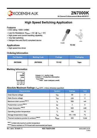
2N7000K N-Channel Enhancement Mode MOSFET High Speed Switching Application Features ESD rating 1000V (HBM) Low On-Resistance RDS(on)
8.18. Size:28K semelab
2n7000csm.pdf 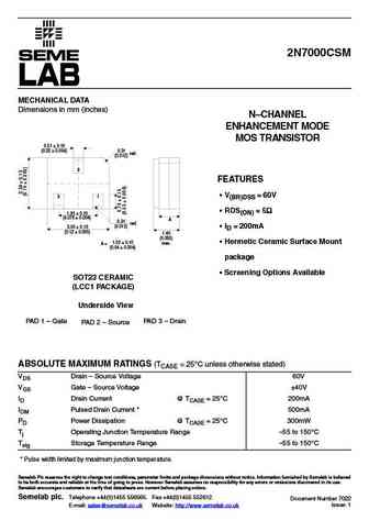
2N7000CSM MECHANICAL DATA Dimensions in mm (inches) N CHANNEL ENHANCEMENT MODE MOS TRANSISTOR 0.51 0.10 (0.02 0.004) 0.31 rad. (0.012) 3 FEATURES V(BR)DSS = 60V 21 RDS(ON) = 5 1.91 0.10 (0.075 0.004) A 0.31 rad. (0.012) 3.05 0.13 ID = 200mA (0.12 0.005) 1.40 (0.055) 1.02 0.10 Hermetic Ceramic Surface Mount max. A = (0.04
8.19. Size:358K secos
2n7000.pdf 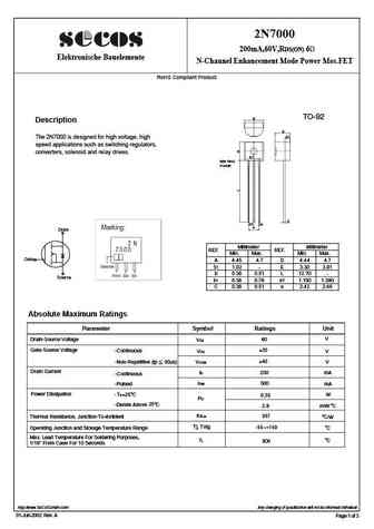
2N7000 200mA,60V,RDS(ON) 6 Elektronische Bauelemente N-Channel Enhancement Mode Power Mos.FET RoHS Compliant Product TO-92 D Description E S1 The 2N7000 is designed for high voltage, high speed applications such as switching regulators, converters, solenoid and relay drives. b1 SEATING PLANE C e1 b e Drain Millimeter Millimeter REF. REF. Min. Max. Min. Max. Gat
8.21. Size:181K taiwansemi
tsm2n7000kct.pdf 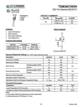
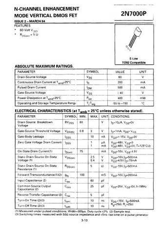
TSM2N7000K 60V N-Channel MOSFET TO-92 Pin Definition PRODUCT SUMMARY 1. Source VDS (V) RDS(on)( ) ID (mA) 2. Gate 3. Drain 5 @ VGS = 10V 100 60 5.5 @ VGS = 5V 100 Features Block Diagram Low On-Resistance ESD Protection High Speed Switching Low Voltage Drive Ordering Information Part No. Package Packing TSM2N7000KCT B0 TO-92 1Kpcs / Bulk
8.22. Size:531K jiangsu
2n7000.pdf 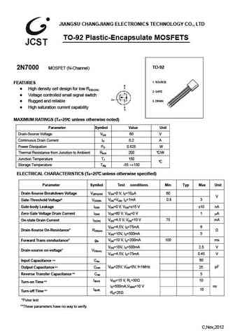
JIANGSU CHANGJIANG ELECTRONICS TECHNOLOGY CO., LTD TO-92 Plastic-Encapsulate MOSFETS TO-92 2N7000 MOSFET (N-Channel) 1. SOURCE FEATURES High density cell design for low RDS(ON) 2. GATE Voltage controlled small signal switch 3. DRAIN Rugged and reliable High saturation current capability MAXIMUM RATINGS (Ta=25 unless otherwise noted) Parameter Symbol Value
8.23. Size:63K kec
2n7000.pdf 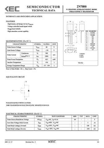
2N7000 SEMICONDUCTOR N CHANNEL ENHANCEMENT MODE TECHNICAL DATA FIELD EFFECT TRANSISTOR INTERFACE AND SWITCHING APPLICATION. B C FEATURES High density cell design for low RDS(ON). Voltage controlled small signal switch. Rugged and reliable. N DIM MILLIMETERS High saturation current capablity. A 4.70 MAX E K B 4.80 MAX G C 3.70 MAX D D 0.45 E 1.00 F 1.27 G 0.85 MAXIMUM RA
8.24. Size:67K kec
2n7000k.pdf 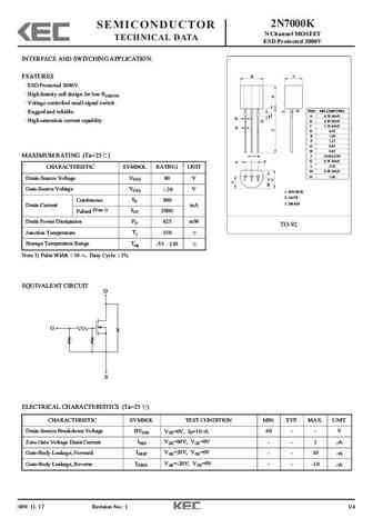
2N7000K SEMICONDUCTOR N Channel MOSFET TECHNICAL DATA ESD Protected 2000V INTERFACE AND SWITCHING APPLICATION. B C FEATURES ESD Protected 2000V. High density cell design for low RDS(ON). Voltage controlled small signal switch. N DIM MILLIMETERS Rugged and reliable. A 4.70 MAX E K B 4.80 MAX High saturation current capablity. G C 3.70 MAX D D 0.45 E 1.00 F 1.27 G 0.85 H
8.25. Size:61K kec
2n7000a.pdf 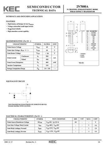
2N7000A SEMICONDUCTOR N CHANNEL ENHANCEMENT MODE TECHNICAL DATA FIELD EFFECT TRANSISTOR INTERFACE AND SWITCHING APPLICATION. B C FEATURES High density cell design for low RDS(ON). Voltage controolled small signal switch. Rugged and reliable. N DIM MILLIMETERS High saturation current capablity. A 4.70 MAX E K B 4.80 MAX G C 3.70 MAX D D 0.45 E 1.00 F 1.27 G 0.85
8.26. Size:239K lge
2n7000.pdf 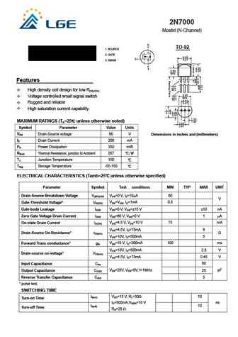
2N7000 Mosfet (N-Channel) TO-92 1. SOURCE 2. GATE 3. DRAIN Features High density cell design for low RDS(ON) Voltage controlled small signal switch Rugged and reliable High saturation current capability MAXIMUM RATINGS (TA=25 unless otherwise noted) Symbol Parameter Value Units VDS Drain-Source voltage 60 V Dimensions in inches and (millimeters) ID Drain Curr
8.27. Size:168K wietron
2n7000.pdf 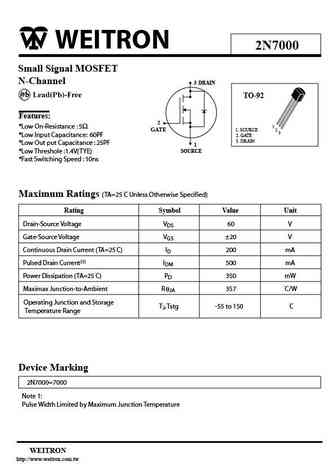
WEITRON 2N7000 Small Signal MOSFET N-Channel 3 DRAIN TO-92 Features 2 1 *Low On-Resistance 5 GATE 1. SOURCE 2 3 *Low Input Capacitance 60PF 2. GATE 3. DRAIN *Low Out put Capacitance 25PF 1 SOURCE *Low Threshole 1.4V(TYE) *Fast Switching Speed 10ns Maximum Ratings (TA=25 C Unless Otherwise Specified) Rating Symbol Value Unit Drain-Source Voltage VDS 60 V Gate-S
8.28. Size:51K hsmc
h2n7000.pdf 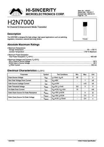
Spec. No. HE6267 HI-SINCERITY Issued Date 1993.09.17 Revised Date 2006.08.10 MICROELECTRONICS CORP. Page No. 1/5 H2N7000 N-Channel Enhancement Mode Transistor Description The H2N7000 is designed for high voltage, high speed applications such as switching regulators, converters, solenoid and relay drivers. TO-92 Absolute Maximum Ratings Maximum Temperatures Storage Temp
8.29. Size:566K semtech
st2n7000.pdf 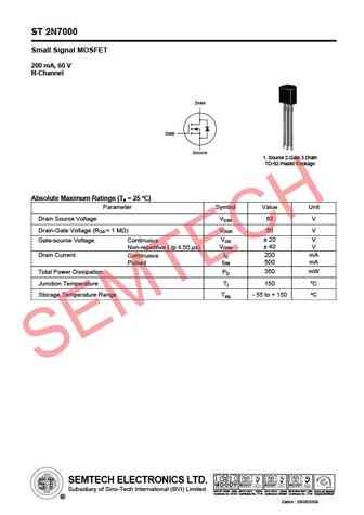
ST 2N7000 Small Signal MOSFET 200 mA, 60 V N-Channel Drain Gate Source 1. Source 2.Gate 3.Drain TO-92 Plastic Package O Absolute Maximum Ratings (Ta = 25 C) Parameter Symbol Value Unit Drain Source Voltage VDSS 60 V Drain-Gate Voltage (RGS = 1 M ) VDGR 60 V Gate-source Voltage Continuous VGS 20 V VGSM 40 V Non-repetitive ( tp 50 s) Drain Current Continuous
8.30. Size:423K shantou-huashan
h2n7000.pdf 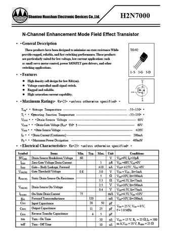
H2N7000 Shantou Huashan Electronic Devices Co.,Ltd. N-Channel Enhancement Mode Field Effect Transistor General Description These products have been designed to minimize on-state resistance While TO-92 provide rugged, reliable, and fast switching performance. These products are particularly suited for low voltage, low current applications such as small servo motor control, pow
8.31. Size:199K inchange semiconductor
2n7000.pdf 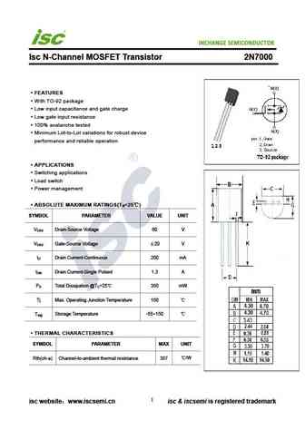
INCHANGE Semiconductor Isc N-Channel MOSFET Transistor 2N7000 FEATURES With TO-92 package Low input capacitance and gate charge Low gate input resistance 100% avalanche tested Minimum Lot-to-Lot variations for robust device performance and reliable operation APPLICATIONS Switching applications Load switch Power management ABSOLUTE MAXIMUM RATINGS(T =25 ) a
Другие IGBT... ZVP3306A, ZVP3306F, ZVP3310A, ZVP3310F, ZVP4105A, ZVP4424A, ZVP4424G, 2N7000BU, 7N60, 2N7002DW, 2N7002K, 2N7002KW, 2N7002MTF, 2N7002T, 2N7002V, 2N7002VA, 2N7002W