13N10. Аналоги и основные параметры
Наименование производителя: 13N10
Тип транзистора: MOSFET
Полярность: N
Предельные значения
Pd ⓘ
- Максимальная рассеиваемая мощность: 105 W
|Vds|ⓘ - Максимально допустимое напряжение сток-исток: 100 V
|Vgs|ⓘ - Максимально допустимое напряжение затвор-исток: 20 V
|Id| ⓘ - Максимально допустимый постоянный ток стока: 18 A
Tj ⓘ - Максимальная температура канала: 175 °C
Электрические характеристики
tr ⓘ -
Время нарастания: 120 ns
Cossⓘ - Выходная емкость: 260 pf
RDSonⓘ - Сопротивление сток-исток открытого транзистора: 0.110 typ Ohm
Тип корпуса: TO220AB
Аналог (замена) для 13N10
- подборⓘ MOSFET транзистора по параметрам
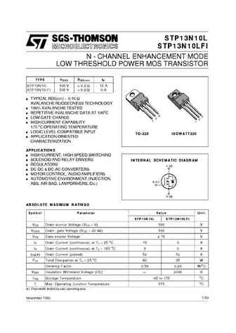
13N10 даташит
..1. Size:672K cn vbsemi
13n10.pdf 
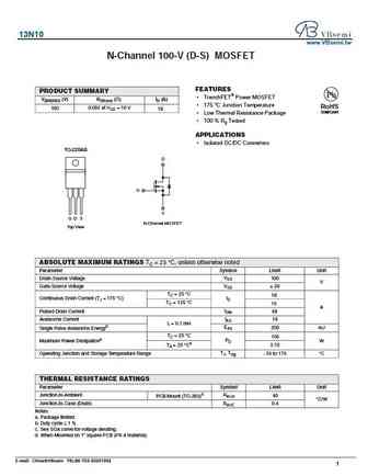
13N10 www.VBsemi.tw N-Channel 100-V (D-S) MOSFET FEATURES PRODUCT SUMMARY TrenchFET Power MOSFET V(BR)DSS (V) RDS(on) ( )ID (A) 175 C Junction Temperature RoHS 0.092 at VGS = 10 V 100 18 COMPLIANT Low Thermal Resistance Package 100 % Rg Tested APPLICATIONS Isolated DC/DC Converters TO-220AB D G S G D S N-Channel MOSFET Top View ABSOLUTE MAXIMU
0.2. Size:554K fairchild semi
fqp13n10l.pdf 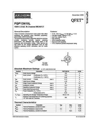
December 2000 TM QFET QFET QFET QFET FQP13N10L 100V LOGIC N-Channel MOSFET General Description Features These N-Channel enhancement mode power field effect 12.8A, 100V, RDS(on) = 0.18 @VGS = 10 V transistors are produced using Fairchild s proprietary, Low gate charge ( typical 8.7 nC) planar stripe, DMOS technology. Low Crss ( typical 20 pF) This advanced technolog
0.3. Size:552K fairchild semi
fqpf13n10l.pdf 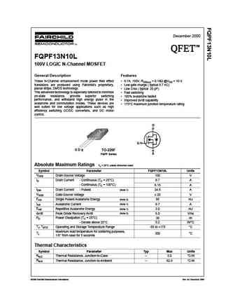
December 2000 TM QFET QFET QFET QFET FQPF13N10L 100V LOGIC N-Channel MOSFET General Description Features These N-Channel enhancement mode power field effect 8.7A, 100V, RDS(on) = 0.18 @VGS = 10 V transistors are produced using Fairchild s proprietary, Low gate charge ( typical 8.7 nC) planar stripe, DMOS technology. Low Crss ( typical 20 pF) This advanced technolog
0.4. Size:714K fairchild semi
fqd13n10tf fqd13n10tm fqd13n10 fqu13n10 fqu13n10tu.pdf 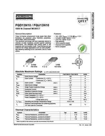
January 2009 QFET FQD13N10 / FQU13N10 100V N-Channel MOSFET General Description Features These N-Channel enhancement mode power field effect 10A, 100V, RDS(on) = 0.18 @VGS = 10 V transistors are produced using Fairchild s proprietary, Low gate charge ( typical 12 nC) planar stripe, DMOS technology. Low Crss ( typical 20 pF) This advanced technology has been especiall
0.5. Size:566K fairchild semi
fqb13n10ltm.pdf 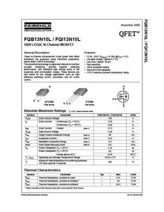
December 2000 TM QFET QFET QFET QFET FQB13N10L / FQI13N10L 100V LOGIC N-Channel MOSFET General Description Features These N-Channel enhancement mode power field effect 12.8A, 100V, RDS(on) = 0.18 @VGS = 10 V transistors are produced using Fairchild s proprietary, Low gate charge ( typical 8.7 nC) planar stripe, DMOS technology. Low Crss ( typical 20 pF) This advanc
0.6. Size:635K fairchild semi
fqb13n10.pdf 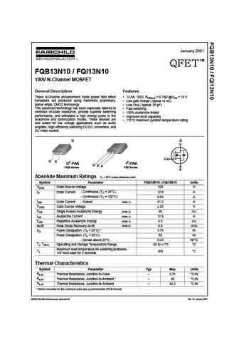
January 2001 TM QFET QFET QFET QFET FQB13N10 / FQI13N10 100V N-Channel MOSFET General Description Features These N-Channel enhancement mode power field effect 12.8A, 100V, RDS(on) = 0.18 @VGS = 10 V transistors are produced using Fairchild s proprietary, Low gate charge ( typical 12 nC) planar stripe, DMOS technology. Low Crss ( typical 20 pF) This advanced technol
0.7. Size:618K fairchild semi
fqp13n10.pdf 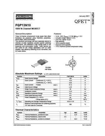
January 2001 TM QFET QFET QFET QFET FQP13N10 100V N-Channel MOSFET General Description Features These N-Channel enhancement mode power field effect 12.8A, 100V, RDS(on) = 0.18 @VGS = 10 V transistors are produced using Fairchild s proprietary, Low gate charge ( typical 12 nC) planar stripe, DMOS technology. Low Crss ( typical 20 pF) This advanced technology has bee
0.8. Size:630K fairchild semi
fqd13n10l fqu13n10l.pdf 
January 2009 QFET FQD13N10L / FQU13N10L 100V LOGIC N-Channel MOSFET General Description Features These N-Channel enhancement mode power field effect 10A, 100V, RDS(on) = 0.18 @VGS = 10 V transistors are produced using Fairchild s proprietary, Low gate charge ( typical 8.7 nC) planar stripe, DMOS technology. Low Crss ( typical 20 pF) This advanced technology is especi
0.9. Size:617K fairchild semi
fqpf13n10.pdf 
January 2001 TM QFET QFET QFET QFET FQPF13N10 100V N-Channel MOSFET General Description Features These N-Channel enhancement mode power field effect 8.7A, 100V, RDS(on) = 0.18 @VGS = 10 V transistors are produced using Fairchild s proprietary, Low gate charge ( typical 12 nC) planar stripe, DMOS technology. Low Crss ( typical 20 pF) This advanced technology has bee
0.10. Size:205K onsemi
ntp13n10-d ntp13n10.pdf 
NTP13N10 Preferred Device Power MOSFET 13 A, 100 V, N-Channel Enhancement-Mode TO-220 Features Source-to-Drain Diode Recovery Time Comparable to a Discrete http //onsemi.com Fast Recovery Diode Avalanche Energy Specified VDSS RDS(ON) TYP ID MAX IDSS and RDS(on) Specified at Elevated Temperature 100 V 165 m @ 10 V 13 A Pb-Free Package is Available Typical Applicat
0.11. Size:984K onsemi
fqd13n10.pdf 
Is Now Part of To learn more about ON Semiconductor, please visit our website at www.onsemi.com Please note As part of the Fairchild Semiconductor integration, some of the Fairchild orderable part numbers will need to change in order to meet ON Semiconductor s system requirements. Since the ON Semiconductor product management systems do not have the ability to manage part nomenclatur
0.12. Size:77K onsemi
ntb13n10-d ntb13n10.pdf 
NTB13N10 Power MOSFET 100 V, 13 A, N-Channel Enhancement-Mode D2PAK Features http //onsemi.com Source-to-Drain Diode Recovery Time Comparable to a Discrete Fast Recovery Diode V(BR)DSS RDS(on) TYP ID MAX Avalanche Energy Specified 100 V 165 mW @ 10 V 13 A IDSS and RDS(on) Specified at Elevated Temperature Mounting Information Provided for the D2PAK Package Pb-Fre
0.13. Size:1231K onsemi
fqd13n10l fqu13n10l.pdf 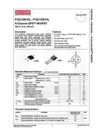
January 2014 FQD13N10L / FQU13N10L N-Channel QFET MOSFET 100 V, 10 A, 180 m Description Features This N-Channel enhancement mode power MOSFET 10 A, 100 V, RDS(on) = 180 m (Max.) @ VGS = 10 V, is produced using Fairchild Semiconductor s proprietary ID = 5.0 A planar stripe and DMOS technology. This advanced Low Gate Charge (Typ. 8.7 nC) MOSFET technology has been
0.14. Size:348K cet
cep13n10 ceb13n10.pdf 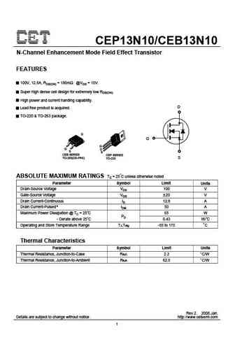
CEP13N10/CEB13N10 N-Channel Enhancement Mode Field Effect Transistor FEATURES 100V, 12.8A, RDS(ON) = 180m @VGS = 10V. Super high dense cell design for extremely low RDS(ON). High power and current handing capability. D Lead free product is acquired. TO-220 & TO-263 package. G CEB SERIES CEP SERIES TO-263(DD-PAK) S TO-220 ABSOLUTE MAXIMUM RATINGS Tc = 25 C unless otherwise noted
0.15. Size:657K cet
cep13n10l ceb13n10l.pdf 
CEP13N10L/CEB13N10L N-Channel Enhancement Mode Field Effect Transistor FEATURES 100V, 12.8A, RDS(ON) = 175m @VGS = 10V. RDS(ON) = 185m @VGS = 5V. Super high dense cell design for extremely low RDS(ON). D High power and current handing capability. Lead free product is acquired. TO-220 & TO-263 package. G CEB SERIES CEP SERIES TO-263(DD-PAK) S TO-220 ABSOLUTE MAXIMUM RATINGS
0.16. Size:535K shantou-huashan
hfp13n10.pdf 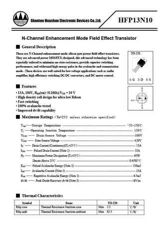
Shantou Huashan Electronic Devices Co.,Ltd. HFP13N10 N-Channel Enhancement Mode Field Effect Transistor General Description These are N-Channel enhancement mode silicon gate power field effect transistors. TO-220 They are advanced power MOSFETs designed, this advanced technology has been especially tailored to minimize on-state resistance, provide superior switching performan
0.17. Size:1086K matsuki electric
me13n10a me13n10a-g.pdf 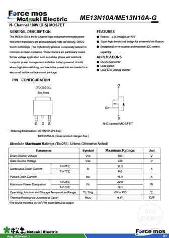
ME13N10A/ME13N10A-G N- Channel 100V (D-S) MOSFET GENERAL DESCRIPTION FEATURES The ME13N10A is the N-Channel logic enhancement mode power RDS(ON) 145m @VGS=10V field effect transistors are produced using high cell density, DMOS Super high density cell design for extremely low RDS(ON) trench technology. This high density process is especially tailored to Exceptional on-res
0.18. Size:302K ncepower
ncep13n10as.pdf 
http //www.ncepower.com NCEP13N10AS NCE N-Channel Super Trench II Power MOSFET Description General Features The NCEP13N10AS uses Super Trench II technology that is VDS =100V,ID =10A uniquely optimized to provide the most efficient high frequency RDS(ON)=12m (typical) @ VGS=10V switching performance. Both conduction and switching power RDS(ON)=15m (typical) @ VGS=4.5V losses
0.19. Size:251K semihow
hrd13n10k.pdf 
Dec 2013 BVDSS = 100 V RDS(on) typ = 85 HRD13N10K / HRU13N10K ID = 3.5 A 100V N-Channel Trench MOSFET D-PAK I-PAK FEATURES 2 1 Originative New Design 1 3 2 3 Superior Avalanche Rugged Technology HRD13N10K HRU13N10K Excellent Switching Characteristics 1.Gate 2. Drain 3. Source Unrivalled Gate Charge 20 nC (Typ.) Extended Safe Operating Area Lower RDS(ON) 8
0.20. Size:987K way-on
wmo13n10ts.pdf 
WMO13N10TS 100V N-Channel Enhancement Mode Power MOSFET Description WMO13N10TS uses advanced power trench technology that has been especially tailored to minimize the on-state resistance and yet maintain superior switching performance. D Features S G V = 100V, I = 13A DS D TO-252 R
0.21. Size:320K cn vanguard
vsd013n10ms.pdf 
VSD013N10MS 100V/52A N-Channel Advanced Power MOSFET V DS 100 V Features R DS(on),TYP@ VGS=10 V 11 m N-Channel R DS(on),TYP@ VGS=4.5 V 12 m Enhancement mode I D 52 A Very low on-resistance RDS(on) @ VGS=4.5 V TO-252 Fast Switching 100% Avalanche test Pb-free lead plating; RoHS compliant Tape and reel Part ID Package Type Marking informat
0.22. Size:757K cn vanguard
vsf013n10ms.pdf 
VSF013N10MS 100V/43A N-Channel Advanced Power MOSFET Features V DS 100 V R DS(on),TYP@ VGS=10 V 10 m Enhancement mode R DS(on),TYP@ VGS=4.5V 11 m Fast Switching I D 43 A Low on-resistance RDS(on) @ VGS=4.5 V TO-220F 100% Avalanche test Pb-free lead plating; RoHS compliant Part ID Package Type Marking Tape and reel information VSF013N10MS TO
0.23. Size:884K cn vbsemi
fqd13n10ltf.pdf 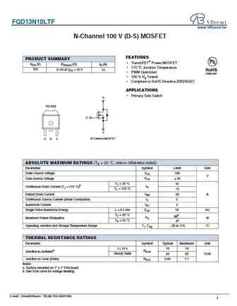
FQD13N10LTF www.VBsemi.tw N-Channel 100 V (D-S) MOSFET FEATURES PRODUCT SUMMARY TrenchFET Power MOSFET VDS (V) RDS(on) ( )ID (A) 175 C Junction Temperature 100 0.11 4 at VGS = 10 V 15 PWM Optimized 100 % Rg Tested Compliant to RoHS Directive 2002/95/EC APPLICATIONS Primary Side Switch D TO-252 G S G D S N-Channel MOSFET ABSOLUTE MAXIMUM RATIN
0.24. Size:1342K cn vbsemi
fqu13n10.pdf 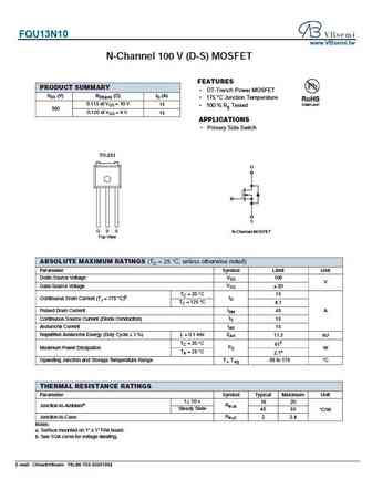
FQU13N10 www.VBsemi.tw N-Channel 100 V (D-S) MOSFET FEATURES PRODUCT SUMMARY DT-Trench Power MOSFET VDS (V) RDS(on) ( )ID (A) 175 C Junction Temperature 0.115 at VGS = 10 V 15 100 % Rg Tested 100 0.120 at VGS = 6 V 15 APPLICATIONS Primary Side Switch TO-251 D G S G D S N-Channel MOSFET Top View ABSOLUTE MAXIMUM RATINGS (TC = 25 C, unless otherwise
0.25. Size:847K cn vbsemi
fqd13n10l.pdf 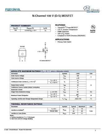
FQD13N10L www.VBsemi.tw N-Channel 100 V (D-S) MOSFET FEATURES PRODUCT SUMMARY TrenchFET Power MOSFET VDS (V) RDS(on) ( )ID (A) 175 C Junction Temperature 100 0.11 4 at VGS = 10 V 15 PWM Optimized 100 % Rg Tested Compliant to RoHS Directive 2002/95/EC APPLICATIONS Primary Side Switch D TO-252 G S G D S N-Channel MOSFET ABSOLUTE MAXIMUM RATING
0.26. Size:1018K cn minos
mdt13n10d.pdf 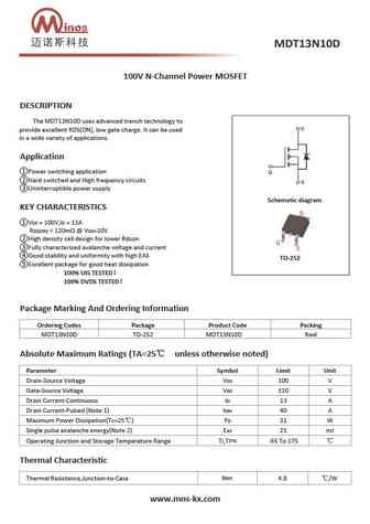
100V N-Channel Power MOSFET DESCRIPTION The MDT13N10D uses advanced trench technology to provide excellent RDS(ON), low gate charge. It can be used in a wide variety of applications. Application Power switching application Hard switched and High frequency circuits Uninterruptible power supply Schematic diagram KEY CHARACTERISTICS VDS = 100V,ID = 13A RDS(ON)
0.27. Size:206K inchange semiconductor
fqp13n10l.pdf 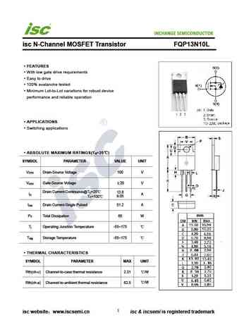
INCHANGE Semiconductor isc N-Channel MOSFET Transistor FQP13N10L FEATURES With low gate drive requirements Easy to drive 100% avalanche tested Minimum Lot-to-Lot variations for robust device performance and reliable operation APPLICATIONS Switching applications ABSOLUTE MAXIMUM RATINGS(T =25 ) a SYMBOL PARAMETER VALUE UNIT V Drain-Source Voltage 100 V DSS V Gate
0.28. Size:278K inchange semiconductor
fqd13n10.pdf 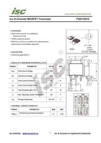
isc N-Channel MOSFET Transistor FQD13N10 FEATURES Static drain-source on-resistance RDS(on) 0.18 100% avalanche tested Minimum Lot-to-Lot variations for robust device performance and reliable operation DESCRITION Switching applications ABSOLUTE MAXIMUM RATINGS(T =25 ) a SYMBOL PARAMETER VALUE UNIT V Drain-Source Voltage 100 V DSS V Gate-Source Voltage 25 V
0.29. Size:239K inchange semiconductor
fqp13n10.pdf 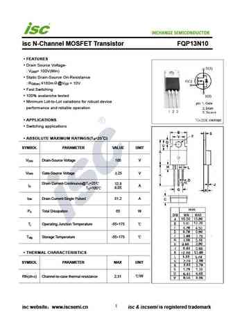
INCHANGE Semiconductor isc N-Channel MOSFET Transistor FQP13N10 FEATURES Drain Source Voltage- V = 100V(Min) DSS Static Drain-Source On-Resistance R 180m @V = 10V DS(on) GS Fast Switching 100% avalanche tested Minimum Lot-to-Lot variations for robust device performance and reliable operation APPLICATIONS Switching applications ABSOLUTE MAXIMUM RATINGS(T
Другие MOSFET... 2SK4067I
, 2SK4068-01
, 2SK4070D
, 2SK4070I
, 2SK4074LS
, 2SK4075B
, 2SK4081
, 2SK4081D
, AON7408
, 15N10-TO251
, 1812
, 1N60L-TM3-T
, 20N03L-TO252
, 20N06L-TO252
, 20N3LG-TO251
, 20P06-TO252
, 25N06L-TN3
.
History: WMN28N65F2
| AOB2144L
| SM1A11NSK