SM2300NSAC. Аналоги и основные параметры
Наименование производителя: SM2300NSAC
Тип транзистора: MOSFET
Полярность: N
Предельные значения
Pd ⓘ - Максимальная рассеиваемая мощность: 1.25 W
|Vds|ⓘ - Максимально допустимое напряжение сток-исток: 20 V
|Vgs|ⓘ - Максимально допустимое напряжение затвор-исток: 12 V
|Id| ⓘ - Максимально допустимый постоянный ток стока: 5 A
Tj ⓘ - Максимальная температура канала: 150 °C
Электрические характеристики
tr ⓘ - Время нарастания: 17 ns
Cossⓘ - Выходная емкость: 105 pf
RDSonⓘ - Сопротивление сток-исток открытого транзистора: 0.028 typ Ohm
Тип корпуса: SOT23
Аналог (замена) для SM2300NSAC
- подборⓘ MOSFET транзистора по параметрам
SM2300NSAC даташит
sm2300nsac.pdf
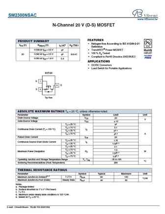
SM2300NSAC www.VBsemi.tw N-Channel 20 V (D-S) MOSFET FEATURES PRODUCT SUMMARY Halogen-free According to IEC 61249-2-21 VDS (V) RDS(on) ( ) ID (A)e Qg (Typ.) Definition 0.028 at VGS = 4.5 V TrenchFET Power MOSFET 6a 100 % Rg Tested 20 0.042 at VGS = 2.5 V 6a 8.8 nC Compliant to RoHS Directive 2002/95/EC 0.050 at VGS = 1.8 V 5.6 APPLICATIONS DC/D
sm2300nsa.pdf
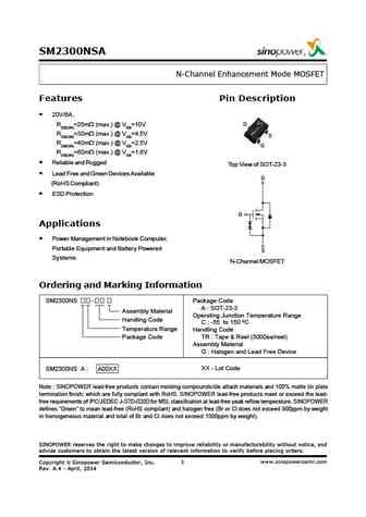
SM2300NSA N-Channel Enhancement Mode MOSFET Features Pin Description 20V/6A , D RDS(ON)=25m (max.) @ VGS=10V RDS(ON)=30m (max.) @ VGS=4.5V S RDS(ON)=40m (max.) @ VGS=2.5V G RDS(ON)=60m (max.) @ VGS=1.8V Reliable and Rugged Top View of SOT-23-3 Lead Free and Green Devices Available D (RoHS Compliant) ESD Protection G Applications Power Management in Notebook Computer
sm2300nsan.pdf
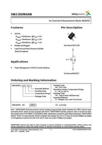
SM2300NSAN N-Channel Enhancement Mode MOSFET Features Pin Description 20V/4A, D RDS(ON)= 40m (max.) @ VGS= 4.5V S RDS(ON)= 55m (max.) @ VGS= 2.5V G RDS(ON)= 85m (max.) @ VGS= 1.8V Top View of SOT-23N Reliable and Rugged Lead Free and Green Devices Available D (RoHS Compliant) G Applications Power Management in DC/AC Inverter Systems. S N-Channel MOSFET
tsm2301a.pdf
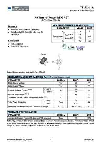
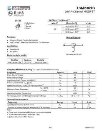
TSM2301A Taiwan Semiconductor P-Channel Power MOSFET -20V, -2.8A, 130m KEY PERFORMANCE PARAMETERS Features PARAMETER VALUE UNIT Advance Trench Process Technology VDS -20 V High Density Cell Design for Ultra Low On- resistance VGS = -4.5V 130 RDS(on) (max) m VGS = -2.5V 190 Application Qg 7.2 nC Telecom power Consumer Electronics SOT-23
tsm2306cx.pdf
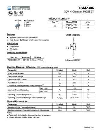
TSM2306 30V N-Channel MOSFET PRODUCT SUMMARY SOT-23 Pin Definition VDS (V) RDS(on)(m ) ID (A) 1. Gate 2. Source 57 @ VGS =10V 3.5 3. Drain 30 94 @ VGS =4.5V 2.8 Features Block Diagram Advance Trench Process Technology High Density Cell Design for Ultra Low On-resistance Application Load Switch PA Switch Ordering Information Part No. Pa
tsm2302 a07.pdf
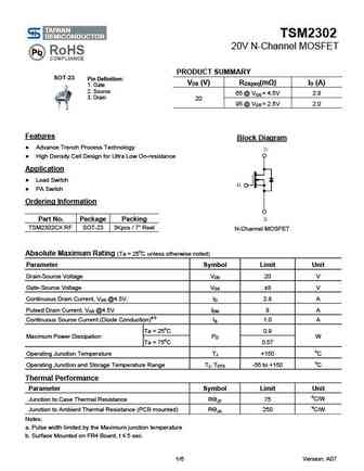
TSM2302 20V N-Channel MOSFET PRODUCT SUMMARY SOT-23 Pin Definition VDS (V) RDS(on)(m ) ID (A) 1. Gate 2. Source 65 @ VGS = 4.5V 2.8 3. Drain 20 95 @ VGS = 2.5V 2.0 Features Block Diagram Advance Trench Process Technology High Density Cell Design for Ultra Low On-resistance Application Load Switch PA Switch Ordering Information Part No.
tsm2307cx.pdf
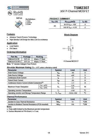
TSM2307 30V P-Channel MOSFET SOT-23 PRODUCT SUMMARY Pin Definition 1. Gate VDS (V) RDS(on)(m ) ID (A) 2. Source 3. Drain 95 @ VGS = -10V -3 -30 140 @ VGS = -4.5V -2 Features Block Diagram Advance Trench Process Technology High Density Cell Design for Ultra Low On-resistance Application Load Switch PA Switch Ordering Information Part No
tsm2308cx.pdf
TSM2308 60V N-Channel MOSFET SOT-23 PRODUCT SUMMARY Pin Definition 1. Gate VDS (V) RDS(on)(m ) ID (A) 2. Source 3. Drain 156 @ VGS = 10V 3 60 192 @ VGS = 4.5V 2.1 Block Diagram Features Advance Trench Process Technology High Density Cell Design for Ultra Low On-resistance Application DC-DC Power System Load Switch Ordering Information
tsm2303cx.pdf
TSM2303 30V P-Channel MOSFET SOT-23 PRODUCT SUMMARY Pin Definition 1. Gate VDS (V) RDS(on)(m ) ID (A) 2. Source 3. Drain 180 @ VGS =-10V -1.3 -30 300 @ VGS =-4.5V -1.1 Block Diagram Features Advance Trench Process Technology High Density Cell Design for Ultra Low On-resistance Application Portable Devices High Speed Switch Ordering Info
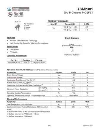
tsm2301acx tsm2301cx.pdf
TSM2301 20V P-Channel MOSFET PRODUCT SUMMARY SOT-23 Pin Definition VDS (V) RDS(on)(m ) ID (A) 1. Gate 130 @ VGS = -4.5V -2.8 2. Source -20 3. Drain 190 @ VGS = -2.5V -2.0 Features Block Diagram Advance Trench Process Technology High Density Cell Design for Ultra Low On-resistance Application Load Switch PA Switch P-Channel MOSFET Orderi
tsm2302cx.pdf
TSM2302 20V N-Channel MOSFET SOT-23 Pin Definition PRODUCT SUMMARY 1. Gate VDS (V) RDS(on)(m ) ID (A) 2. Source 3. Drain 65 @ VGS = 4.5V 2.8 20 95 @ VGS = 2.5V 2.0 Features Block Diagram Advance Trench Process Technology High Density Cell Design for Ultra Low On-resistance Application Load Switch PA Switch Ordering Information Part No.
tsm2305cx.pdf
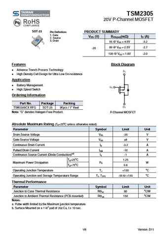
TSM2305 20V P-Channel MOSFET SOT-23 PRODUCT SUMMARY Pin Definition 1. Gate VDS (V) RDS(on)(m ) ID (A) 2. Source 3. Drain 55 @ VGS =-4.5V -3.2 80 @ VGS =-2.5V -2.7 -20 130 @ VGS =-1.8V -2.0 Block Diagram Features Advance Trench Process Technology High Density Cell Design for Ultra Low On-resistance Application Battery Management High Spe
sm2306nsa.pdf

SM2306NSA N-Channel Enhancement Mode MOSFET Features Pin Description 30V/4.7A, D RDS(ON)=40m (max.) @ VGS=10V S RDS(ON)=60m (max.) @ VGS=4.5V G Reliable and Rugged Lead Free and Green Devices Available Top View of SOT-23-3 (RoHS Compliant) D Applications G Power Management in Notebook Computer, Portable Equipment and Battery Powered Systems. S Load Switch N-Chann
sm2302nsa.pdf
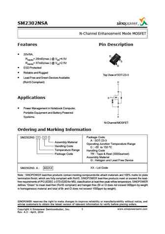
SM2302NSA N-Channel Enhancement Mode MOSFET Features Pin Description 20V/6A, D RDS(ON)= 26m (max.) @ VGS=4.5V S RDS(ON)= 37m (max.) @ VGS=2.5V G ESD Protected Reliable and Rugged Top View of SOT-23-3 Lead Free and Green Devices Available D (RoHS Compliant) G Applications Power Management in Notebook Computer, Portable Equipment and Battery Powered S Systems. N-Chan
sm2303psa.pdf
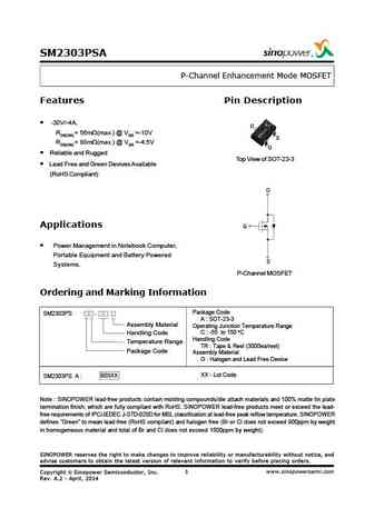
SM2303PSA P-Channel Enhancement Mode MOSFET Features Pin Description -30V/-4A, D RDS(ON) = 56m (max.) @ VGS =-10V S RDS(ON) = 88m (max.) @ VGS =-4.5V G Reliable and Rugged Top View of SOT-23-3 Lead Free and Green Devices Available (RoHS Compliant) D Applications G Power Management in Notebook Computer, Portable Equipment and Battery Powered S Systems. P-Channel MOSFE
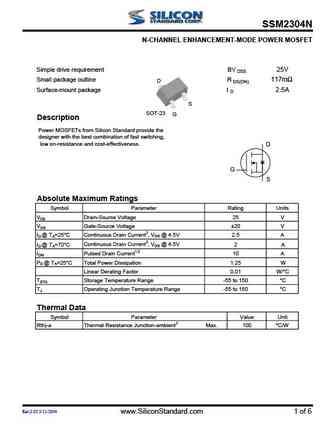
sm2304nsa.pdf
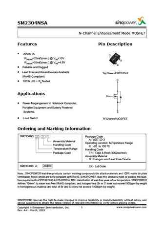
SM2304NSA N-Channel Enhancement Mode MOSFET Features Pin Description 30V/5.1A, D RDS(ON)=25m (max.) @ VGS=10V S RDS(ON)=35m (max.) @ VGS=4.5V G Reliable and Rugged Lead Free and Green Devices Available Top View of SOT-23-3 (RoHS Compliant) D 100% UIS + Rg Tested Applications G Power Magangement in Notebook Computer, Portable Equipment and Battery Powered Sys
sm2307psa.pdf
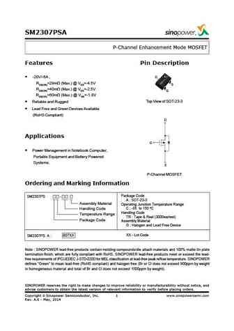
SM2307PSA P-Channel Enhancement Mode MOSFET Features Pin Description -20V/-6A , D RDS(ON)=29m (Max.) @ VGS=-4.5V S RDS(ON)=40m (Max.) @ VGS=-2.5V G RDS(ON)=60m (Max.) @ VGS=-1.8V Top View of SOT-23-3 Reliable and Rugged Lead Free and Green Devices Available (RoHS Compliant) D Applications G Power Management in Notebook Computer, Portable Equipment and Battery Powered
sm2305psa.pdf

SM2305PSA P-Channel Enhancement Mode MOSFET Features Pin Description -20V/-4.9A , D RDS(ON)=43m (Max.) @ VGS=-4.5V S RDS(ON)=58m (Max.) @ VGS=-2.5V G RDS(ON)=88m (Max.) @ VGS=-1.8V Top View of SOT-23 100% UIS + Rg Tested Reliable and Rugged Lead Free and Green Devices Available D (RoHS Compliant) Applications G Power Management in Notebook Computer, Po
sm2309psa.pdf

SM2309PSA P-Channel Enhancement Mode MOSFET Features Pin Description -30V/-3.1A, D RDS(ON) = 95m (max.) @ VGS =-10V S RDS(ON) = 150m (max.) @ VGS =-4.5V G Reliable and Rugged Top View of SOT-23-3 Lead Free and Green Devices Available (RoHS Compliant) D G Applications Power Management in Notebook Computer, Portable Equipment and Battery Powered S Systems. P-Channel MO
sm2308nsa.pdf
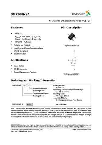
SM2308NSA N-Channel Enhancement Mode MOSFET Features Pin Description 30V/5.2A , D RDS(ON)= 35m (max.) @ VGS=10V S RDS(ON)= 45m (max.) @ VGS=4.5V G 100% UIS + Rg Tested Reliable and Rugged Top View of SOT-23 Lead Free and Green Devices Available (RoHS Compliant) D ESD Protection G Applications Load Switch. DC-DC converter. S Power Management Function. N-Channel
gsm2303a.pdf
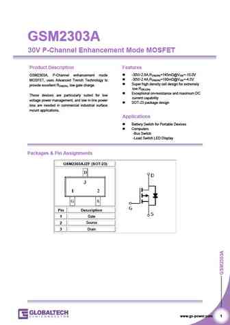
GSM2303A GSM2303A 30V P-Channel Enhancement Mode MOSFET Product Description Features -30V/-2.8A,RDS(ON)=145m @VGS=-10.0V GSM2303A, P-Channel enhancement mode -30V/-2.4A,RDS(ON)=180m @VGS=-4.5V MOSFET, uses Advanced Trench Technology to Super high density cell design for extremely provide excellent RDS(ON), low gate charge. low RDS (ON) Exceptional on-res
gsm2301as.pdf
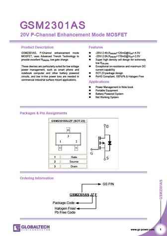
20V P-Channel Enhancement Mode MOSFET Product Description Features GSM2301AS, P-Channel enhancement mode -20V/-2.4A,RDS(ON)=125m @VGS=-4.5V MOSFET, uses Advanced Trench Technology to -20V/-2.0A,RDS(ON)=170m @VGS=-2.5V provide excellent RDS(ON), low gate charge. Super high density cell design for extremely low RDS (ON) These devices are particularly suited for low voltage
gsm2304a.pdf
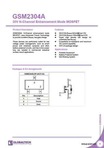
GSM2304A 30V N-Channel Enhancement Mode MOSFET Product Description Features GSM2304A, N-Channel enhancement mode 30V/2.6A,RDS(ON)=82m @VGS=10V MOSFET, uses Advanced Trench Technology 30V/2.0A,RDS(ON)=108m @VGS=4.5V to provide excellent RDS(ON), low gate charge. Super high density cell design for extremely low RDS (ON) These devices are particularly suited for low Exce
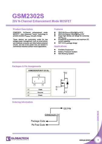
gsm2302as.pdf
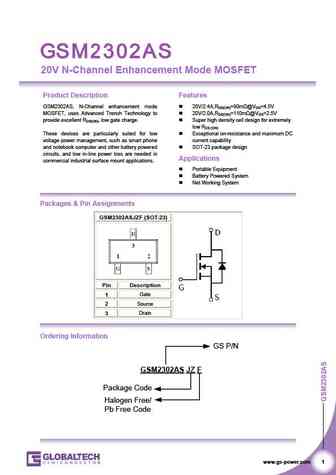
20V N-Channel Enhancement Mode MOSFET Product Description Features GSM2302AS, N-Channel enhancement mode 20V/2.4A,RDS(ON)=90m @VGS=4.5V MOSFET, uses Advanced Trench Technology to 20V/2.0A,RDS(ON)=110m @VGS=2.5V provide excellent RDS(ON), low gate charge. Super high density cell design for extremely low RDS (ON) These devices are particularly suited for low Exceptional on-
gsm2301s.pdf
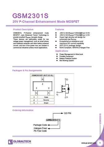
20V P-Channel Enhancement Mode MOSFET Product Description Features GSM2301S, P-Channel enhancement mode -20V/-2.8A,RDS(ON)=120m @VGS=-4.5V MOSFET, uses Advanced Trench Technology to -20V/-2.0A,RDS(ON)=170m @VGS=-2.5V provide excellent RDS(ON), low gate charge. Super high density cell design for These devices are particularly suited for low extremely low RDS (ON) volt
gsm2309a.pdf
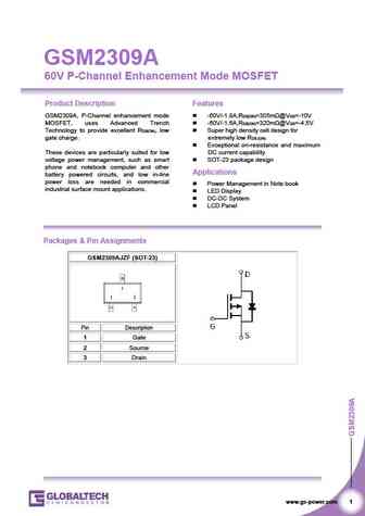
GSM2309A 60V P-Channel Enhancement Mode MOSFET Product Description Features GSM2309A, P-Channel enhancement mode -60V/-1.8A,RDS(ON)=305m @VGS=-10V MOSFET, uses Advanced Trench -60V/-1.6A,RDS(ON)=320m @VGS=-4.5V Technology to provide excellent RDS(ON), low Super high density cell design for gate charge. extremely low RDS (ON) Exceptional on-resistance and maxim
gsm2309.pdf
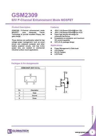
GSM2309 60V P-Channel Enhancement Mode MOSFET Product Description Features GSM2309, P-Channel enhancement mode -60V/-1.8A,RDS(ON)=305m @VGS=-10V MOSFET, uses Advanced Trench -60V/-1.4A,RDS(ON)=320m @VGS=-4.5V Technology to provide excellent RDS(ON), low Super high density cell design for gate charge. extremely low RDS (ON) Exceptional on-resistance and maximum
gsm2301a.pdf
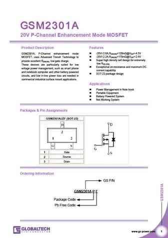
20V P-Channel Enhancement Mode MOSFET Product Description Features -20V/-2.6A,RDS(ON)=120m @VGS=-4.5V GSM2301A, P-Channel enhancement mode -20V/-2.2A,RDS(ON)=170m @VGS=-2.5V MOSFET, uses Advanced Trench Technology to Super high density cell design for extremely provide excellent RDS(ON), low gate charge. low RDS (ON) These devices are particularly suited for low
gsm2301.pdf
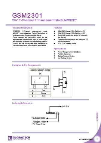
20V P-Channel Enhancement Mode MOSFET Product Description Features GSM2301, P-Channel enhancement mode -20V/-3.0A,RDS(ON)=105m @VGS=-4.5V MOSFET, uses Advanced Trench Technology to -20V/-2.4A,RDS(ON)=155m @VGS=-2.5V provide excellent RDS(ON), low gate charge. Super high density cell design for extremely These devices are particularly suited for low low RDS (ON) volta
gsm2306a.pdf
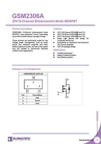
GSM2306A 20V N-Channel Enhancement Mode MOSFET Product Description Features GSM2306A, N-Channel enhancement mode 20V/1.8A,RDS(ON)=280m @VGS=4.5V MOSFET, uses Advanced Trench Technology 20V/1.5A,RDS(ON)=340m @VGS=2.5V to provide excellent RDS(ON), low gate charge. 20V/1.2A,RDS(ON)=750m @VGS=1.8V Super high density cell design for These devices are particularl
gsm2304.pdf
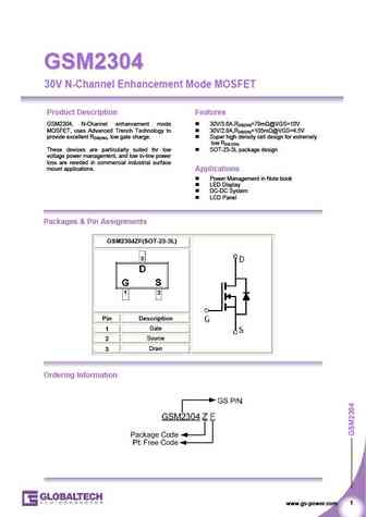
GSM2304 GSM2304 30V N-Channel Enhancement Mode MOSFET Product Description Features GSM2304, N-Channel enhancement mode 30V/3.6A,RDS(ON)=78m @VGS=10V MOSFET, uses Advanced Trench Technology to 30V/2.8A,RDS(ON)=105m @VGS=4.5V provide excellent RDS(ON), low gate charge. Super high density cell design for extremely low RDS (ON) These devices are particularly suited for low
gsm2304as.pdf
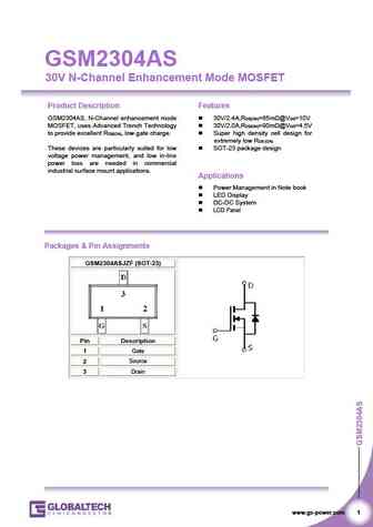
GSM2304AS 30V N-Channel Enhancement Mode MOSFET Product Description Features GSM2304AS, N-Channel enhancement mode 30V/2.4A,RDS(ON)=65m @VGS=10V MOSFET, uses Advanced Trench Technology 30V/2.0A,RDS(ON)=90m @VGS=4.5V to provide excellent RDS(ON), low gate charge. Super high density cell design for extremely low RDS (ON) These devices are particularly suited for low SOT-2
gsm2307a.pdf
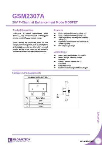
GSM2307A GSM2307A 20V P-Channel Enhancement Mode MOSFET Product Description Features -20V/-1.8A,RDS(ON)=520m @VGS=-4.5V GSM2307A, P-Channel enhancement mode -20V/-1.5A,RDS(ON)=870m @VGS=-2.5V MOSFET, uses Advanced Trench Technology to Super high density cell design for extremely provide excellent RDS(ON), low gate charge. low RDS (ON) Exceptional on-resi
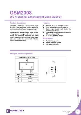
gsm2308a.pdf
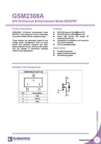
GSM2308A 60V N-Channel Enhancement Mode MOSFET Product Description Features GSM2308A, N-Channel enhancement mode 60V/2.8A,RDS(ON)=135m @VGS=10V MOSFET, uses Advanced Trench Technology 60V/2.0A,RDS(ON)=145m @VGS=4.5V to provide excellent RDS(ON), low gate charge. Super high density cell design for extremely low RDS (ON) These devices are particularly suited for low
gsm2303.pdf
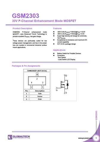
GSM2303 GSM2303 30V P-Channel Enhancement Mode MOSFET Product Description Features -30V/-3.6A,RDS(ON)=130m @VGS=-10.0V GSM2303, P-Channel enhancement mode -30V/-3.2A,RDS(ON)=170m @VGS=-4.5V MOSFET, uses Advanced Trench Technology to Super high density cell design for extremely provide excellent RDS(ON), low gate charge. low RDS (ON) Exceptional on-resist
gsm2306ae.pdf
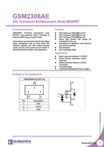
GSM2306AE 20V N-Channel Enhancement Mode MOSFET Product Description Features GSM2306AE, N-Channel enhancement mode 20V/1.8A,RDS(ON)=280m @VGS=4.5V MOSFET, uses Advanced Trench Technology to 20V/1.5A,RDS(ON)=340m @VGS=2.5V provide excellent RDS(ON), low gate charge. 20V/1.2A,RDS(ON)=750m @VGS=1.8V Super high density cell design for These devices are particula
gsm2302s.pdf
GSM2302S GSM2302S 20V N-Channel Enhancement Mode MOSFET Product Description Features GSM2302S, N-Channel enhancement mode 20V/3.6A,RDS(ON)=85m @VGS=4.5V MOSFET, uses Advanced Trench Technology to 20V/3.2A,RDS(ON)=100m @VGS=2.5V provide excellent RDS(ON), low gate charge. Super high density cell design for extremely low RDS (ON) These devices are particularly suited for
gsm2304s.pdf
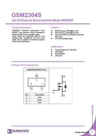
GSM2304S 30V N-Channel Enhancement Mode MOSFET Product Description Features GSM2304S, N-Channel enhancement mode 30V/3.6A,RDS(ON)=60m @VGS=10V MOSFET, uses Advanced Trench Technology to 30V/2.5A,RDS(ON)=85m @VGS=4.5V provide excellent RDS(ON) ,low gate charge. Super high density cell design for extremely These devices are particularly suited for low low RDS (O
ssm2306gn.pdf
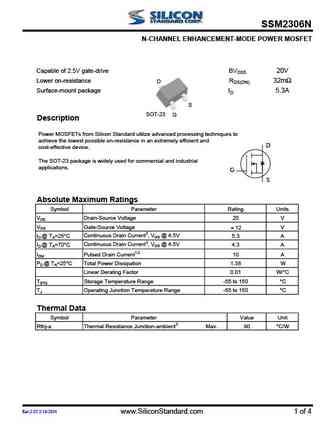
SSM2306N N-CHANNEL ENHANCEMENT-MODE POWER MOSFET Capable of 2.5V gate-drive BVDSS 20V Lower on-resistance RDS(ON) 32m D Surface-mount package ID 5.3A S SOT-23 G Description Power MOSFETs from Silicon Standard utilize advanced processing techniques to achieve the lowest possible on-resistance in an extremely efficient and D cost-effective device. The SOT-23 package is widely use
ssm2309gn.pdf

SSM2309GN P-channel Enhancement-mode Power MOSFET Low gate-charge BVDSS -30V D Simple drive requirement R 75m DS(ON) Fast switching ID -3.7A G Pb-free; RoHS compliant. S DESCRIPTION D The SSM2309GN is in a SOT-23-3 package, which is widely used for lower power commercial and industrial surface mount applications. It is well suited S for low voltage applications such as DC/DC c
ssm2307gn.pdf
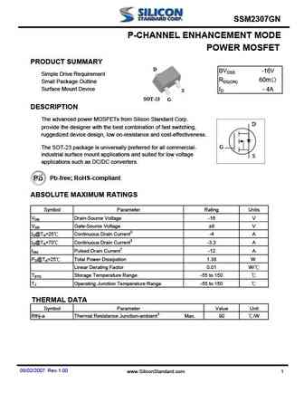
SSM2307GN P-CHANNEL ENHANCEMENT MODE POWER MOSFET PRODUCT SUMMARY D BVDSS -16V Simple Drive Requirement RDS(ON) 60m Small Package Outline Surface Mount Device ID - 4A S SOT-23 G DESCRIPTION The advanced power MOSFETs from Silicon Standard Corp. D provide the designer with the best combination of fast switching, ruggedized device design, low on-resistance and cost-effec
ssm2304agn.pdf
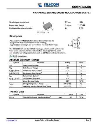
SSM2304AGN N-CHANNEL ENHANCEMENT-MODE POWER MOSFET Simple drive requirement BV 30V DSS D Lower gate charge R 117m DS(ON) Fast switching characteristics ID 2.5A S SOT-23-3 G Description D Advanced Power MOSFETs from Silicon Standard provide the designer with the best combination of fast switching, ruggedized device design, low on-resistance and cost-effectiveness. G S The SS
ssm2303gn.pdf
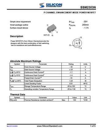
SSM2303N P-CHANNEL ENHANCEMENT-MODE POWER MOSFET Simple drive requirement BVDSS -30V Small package outline RDS(ON) 240m D Surface-mount device ID - 1.7A S SOT-23 G Description D Power MOSFETs from Silicon Standard provide the designer with the best combination of fast switching, low on-resistance and cost-effectiveness. G S Absolute Maximum Ratings Symbol Parameter Rating Un
ssm2302gn.pdf

SSM2302N N-CHANNEL ENHANCEMENT-MODE POWER MOSFET Capable of 2.5V gate drive BVDSS 20V Small package outline RDS(ON) 85m D Surface-mount package ID 2.8A S SOT-23 G Description Power MOSFETs from Silicon Standard provide the designer with the best combination of fast switching, D low on-resistance and cost-effectiveness. G S Absolute Maximum Ratings Symbol Parameter Rating Uni
ssm2305gn.pdf
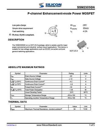
SSM2305GN P-channel Enhancement-mode Power MOSFET Low gate-charge BVDSS -20V D Simple drive requirement R 65m DS(ON) Fast switching ID -4.2A G Pb-free; RoHS compliant. S DESCRIPTION D The SSM2305GN is in a SOT-23-3 package, which is widely used for lower power commercial and industrial surface mount applications. This device is S suitable for low-voltage applications such as
ssm2301gn.pdf
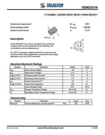
SSM2301N P-CHANNEL ENHANCEMENT-MODE POWER MOSFET Simple drive requirement BV -20V DSS Small package outline RDS(ON) 130m D Surface-mount device ID -2.3A S SOT-23 G Description D Power MOSFETs from Silicon Standard Corp. provide the designer with the best combination of fast switching, low G on-resistance and cost-effectiveness. S The SOT-23 package is widely preferred for co
ssm2304gn.pdf
SSM2304N N-CHANNEL ENHANCEMENT-MODE POWER MOSFET Simple drive requirement BV 25V DSS Small package outline R 117m D DS(ON) Surface-mount package I 2.5A D S SOT-23 G Description Power MOSFETs from Silicon Standard provide the designer with the best combination of fast switching, low on-resistance and cost-effectiveness. D G S Absolute Maximum Ratings Symbol Parameter Rati
ssm2305agn.pdf

SSM2305AGN P-channel Enhancement-mode Power MOSFET Low gate-charge BVDSS -30V D Simple drive requirement R 80m DS(ON) Fast switching ID -3.2A G Pb-free; RoHS compliant. S DESCRIPTION D The SSM2305AGN is in a SOT-23-3 package, which is widely used for lower power commercial and industrial surface mount applications. This device is S suitable for low-voltage applications such a
jsm2302.pdf
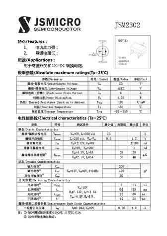
JSM2302 /Features 1 2 /Applications DC-DC /Absolute maximum ratings(Ta=25 ) /Parameter / Symbol /Value /Unit - /Drain-Source Voltage V 20 V DS - /Gate-Source Voltage V 12 V GS /C
jsm2301s.pdf
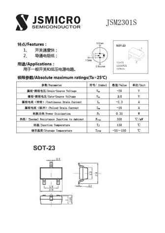
JSM2301S /Features 1 2 /Applications /Absolute maximum ratings(Ta=25 ) /Parameter / Symbol /Value /Unit - /Drain-Source Voltage V -20 V DS - /Gate-Source Voltage V 8 V GS /C
sm2301.pdf
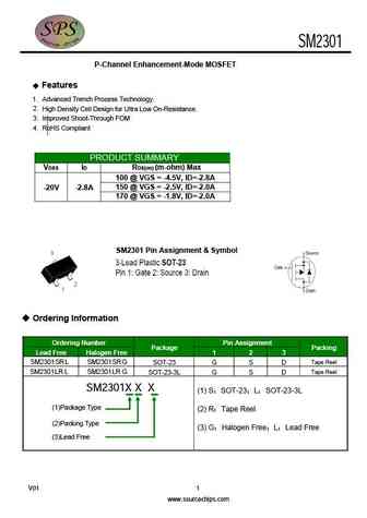
SM2301 P-Channel Enhancement-Mode MOSFET Features 1 Advanced Trench Process Technology. 2 High Density Cell Design for Ultra Low On-Resistance. 3 Improved Shoot-Through FOM 4 RoHS Compliant PRODUCT SUMMARY VDSS ID RDS(on) (m-ohm) Max 100 @ VGS = -4.5V, ID=-2.8A 150 @ VGS = -2.5V, ID=-2.0A -20V -2.8A 170 @ VGS = -1.8V, ID=-2.0A SM2301 Pin Assignment &
sm2305.pdf
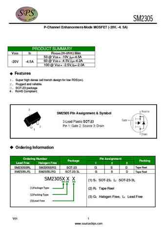
SM2305 P-Channel Enhancement-Mode MOSFET (-20V, -4. 5A) PRODUCT SUMMARY VDSS ID RDS(on) (m-ohm) Max 53 @ VGS = -10V,ID=-4.5A 60 @ VGS = -4.5V,ID=-4.2A -20V -4.5A 100 @ VGS = -2.5V,ID=-2.0A Features 1 Super high dense cell trench design for low RDS(on). 2 Rugged and reliable. 3 SOT-23 package 4 RoHS Compliant. SM2305 Pin Assignment & Symbol
sm2302.pdf
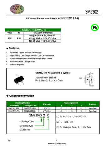
SM2302 N-Channel Enhancement-Mode MOSFET(20V, 2.8A) Pb PRODUCT SUMMARY VDSS ID RDS(on) (m-ohm) Max 60 @ VGS = 4.5V, ID=2.8A 20V 2.8A 115 @ VGS = 2.5V, ID=2.0A 130 @ VGS = 1.8V, ID=2.0A Features 1 Advanced Trench Process Technology. 2 High Density Cell Design for Ultra Low On-Resistance. 3 Fully Characterized Avalanche Voltage and Current. 4 Improved Shoot
sm2306.pdf
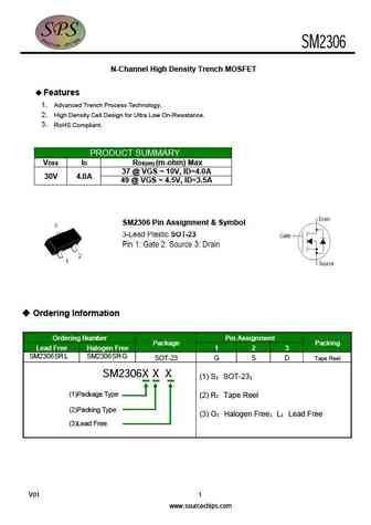
SM2306 N-Channel High Density Trench MOSFET Features 1 Advanced Trench Process Technology. 2 High Density Cell Design for Ultra Low On-Resistance. 3 RoHS Compliant. PRODUCT SUMMARY VDSS ID RDS(on) (m-ohm) Max 37 @ VGS = 10V, ID=4.0A 30V 4.0A 49 @ VGS = 4.5V, ID=3.5A SM2306 Pin Assignment & Symbol Ordering Information Ordering Number Pin Ass
ssm2307g.pdf
SSM2307G www.VBsemi.tw P-Channel 20-V (D-S) MOSFET FEATURES MOSFET PRODUCT SUMMARY Halogen-free According to IEC 61249-2-21 VDS (V) RDS(on) ( )ID (A)a Qg (Typ.) Definition 0.035 at VGS = - 10 V - 5e TrenchFET Power MOSFET e - 20 0.043 at VGS = - 4.5 V - 5 10 nC 100 % Rg Tested 0.061 at VGS = - 2.5 V - 4.8 Compliant to RoHS Directive 2002/95/EC APPLICATION
Другие MOSFET... SI7478DP-T1 , SI9410BDY-T1 , SI9933ADY , SI9948AEY-T1-E3 , SI9955DY , SIR422DP-T1-GE3 , SIR462DP-T1 , SIR802DP-T1-GE3 , RFP50N06 , SM3113NSUC , SM4028NSUC-TRG , SM4307PSKPC , SM4927BSKC , SM4953KC , SP8K1TB , SP8M3-TB , SPD09N05 .
History: 2N7081-220M-ISO | STD20NF06T4
History: 2N7081-220M-ISO | STD20NF06T4
🌐 : EN ES РУ

Список транзисторов
Обновления
MOSFET: ASU70R600E | ASU65R850E | ASU65R550E | ASU65R350E | ASR65R120EFD | ASR65R046EFD | ASQ65R046EFD | ASM65R280E | ASM60R330E | ASE70R950E | ASD80R750E | ASD70R950E | ASD70R600E | ASD70R380E | ASD65R850E | ASD65R550E
Popular searches
bc107 transistor | rjp63g4 datasheet | 2sc1115 | c3998 transistor | 2sa679 | 2sc3181 | 2sb324 | 2sc1904