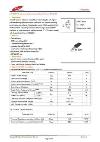
12N60L-T3P-T datasheet, аналоги, основные параметры
Наименование производителя: 12N60L-T3P-T 📄📄
Тип транзистора: MOSFET
Полярность: N
Предельные значения
Pd ⓘ - Максимальная рассеиваемая мощность: 260 W
|Vds|ⓘ - Максимально допустимое напряжение сток-исток: 600 V
|Vgs|ⓘ - Максимально допустимое напряжение затвор-исток: 30 V
|Id| ⓘ - Максимально допустимый постоянный ток стока: 12 A
Tj ⓘ - Максимальная температура канала: 150 °C
Электрические характеристики
tr ⓘ - Время нарастания: 115 ns
Cossⓘ - Выходная емкость: 200 pf
RDSonⓘ - Сопротивление сток-исток открытого транзистора: 0.8 Ohm
Тип корпуса: TO-3P
📄📄 Копировать
Аналог (замена) для 12N60L-T3P-T
- подборⓘ MOSFET транзистора по параметрам
12N60L-T3P-T даташит
12n60l-ta3-t 12n60g-ta3-t 12n60l-tf1-t 12n60g-tf1-t 12n60l-tf2-t 12n60g-tf2-t 12n60l-tf3-t 12n60g-tf3-t 12n60l-t2q-t 12n60g-t2q-t 12n60l-t3p-t 12n60g-t3p-t.pdf
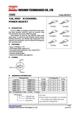
UNISONIC TECHNOLOGIES CO., LTD 12N60 Power MOSFET 12A, 600V N-CHANNEL POWER MOSFET DESCRIPTION The UTC 12N60 are N-Channel enhancement mode power field effect transistors (MOSFET) which are produced using UTC s proprietary, planar stripe, DMOS technology. These devices are suited for high efficiency switch mode power supply. To minimize on-state resistance, provide supe
hgtp12n60d1.pdf
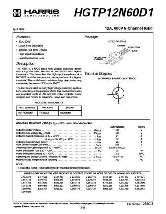
S E M I C O N D U C T O R HGTP12N60D1 12A, 600V N-Channel IGBT April 1995 Features Package JEDEC TO-220AB 12A, 600V EMITTER Latch Free Operation COLLECTOR Typical Fall Time
fhp12n60.pdf
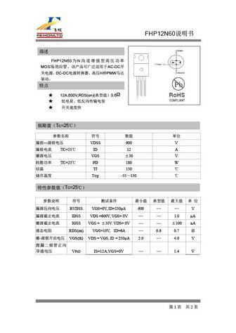
FHP12N60 FHP12N60 N MOS AC-DC DC-DC H PMW 12A,600V,RDS(on)( 0.6 TC=25 VDS
hgtp12n60a4 hgtg12n60a4 hgt1s12n60a4s.pdf
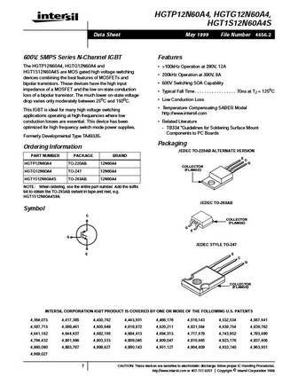
HGTP12N60A4, HGTG12N60A4, HGT1S12N60A4S Data Sheet May 1999 File Number 4656.2 600V, SMPS Series N-Channel IGBT Features The HGTP12N60A4, HGTG12N60A4 and >100kHz Operation at 390V, 12A HGT1S12N60A4S are MOS gated high voltage switching 200kHz Operation at 390V, 9A devices combining the best features of MOSFETs and 600V Switching SOA Capability bipolar transistors. These de
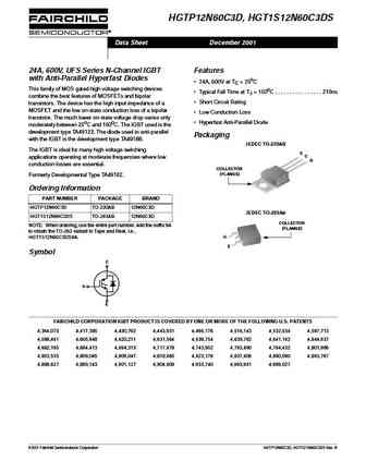
hgt1s12n60c3s9a.pdf
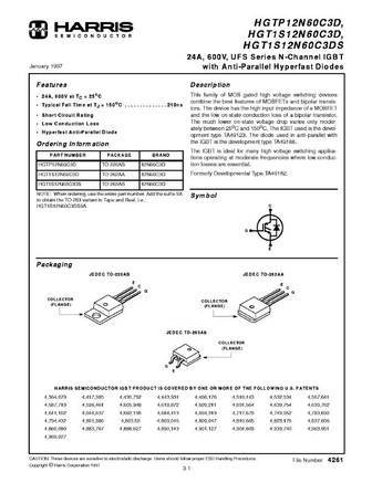
HGTP12N60C3, HGT1S12N60C3S Data Sheet December 2001 24A, 600V, UFS Series N-Channel IGBTs Features The HGTP12N60C3 and HGT1S12N60C3S are MOS gated 24A, 600V at TC = 25oC high voltage switching devices combining the best features 600V Switching SOA Capability of MOSFETs and bipolar transistors. These devices have the Typical Fall Time. . . . . . . . . . . . . . . . 230ns a
stp12n60m2.pdf
STP12N60M2 N-channel 600 V, 0.395 typ., 9 A MDmesh M2 Power MOSFET in a TO-220 package Datasheet - production data Features Order code V R max. I P DS DS(on) D TOT STP12N60M2 600 V 0.450 9 A 85 W Extremely low gate charge Excellent output capacitance (COSS) profile 100% avalanche tested Zener-protected Applications Switching applications F
std12n60dm2ag.pdf
STD12N60DM2AG Datasheet Automotive-grade N-channel 600 V, 380 m typ., 10 A MDmesh DM2 Power MOSFET in a DPAK package Features VDS @ TJmax RDS(on ) max. ID Order code TAB STD12N60DM2AG 650 V 430 m 10 A 3 2 1 DPAK AEC-Q101 qualified Fast-recovery body diode Extremely low gate charge and input capacitance D(2, TAB) Low on-resistance 100% avalanche test
stfi12n60m2.pdf
STFI12N60M2 N-channel 600 V, 0.395 typ., 9 A MDmesh M2 Power MOSFET in an I PAKFP package Datasheet - production data Features Order code V R max. I P DS DS(on) D TOT STFI12N60M2 600 V 0.450 9 A 25 W Extremely low gate charge Excellent output capacitance (COSS) profile 100% avalanche tested Zener-protected Applications Switching application
stf12n60m2.pdf
STF12N60M2 N-channel 600 V, 0.395 typ., 9 A MDmesh M2 Power MOSFET in a TO-220FP package Datasheet - production data Features Order code V R max. I P DS DS(on) D TOT STF12N60M2 600 V 0.450 9 A 25 W Extremely low gate charge Excellent output capacitance (COSS) profile 3 100% avalanche tested 2 Zener-protected 1 Applications TO-220FP Switch
stu12n60m2.pdf
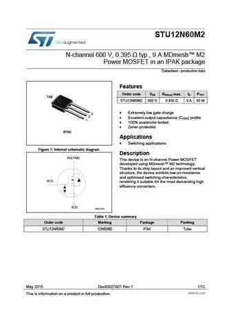
STU12N60M2 N-channel 600 V, 0.395 typ., 9 A MDmesh M2 Power MOSFET in an IPAK package Datasheet - production data Features Order code V R max. I P DS DS(on) D TOT TAB STU12N60M2 600 V 0.450 9 A 85 W Extremely low gate charge 3 2 Excellent output capacitance (COSS) profile 1 100% avalanche tested Zener-protected IPAK Applications Switchi
stl12n60m2.pdf
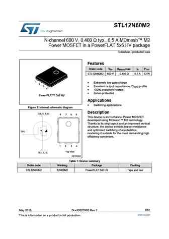
STL12N60M2 N-channel 600 V, 0.400 typ., 6.5 A MDmesh M2 Power MOSFET in a PowerFLAT 5x6 HV package Datasheet - production data Features Order code V R max. I P DS DS(on) D TOT STL12N60M2 600 V 0.495 6.5 A 52 W 1 Extremely low gate charge 2 3 Excellent output capacitance (COSS) profile 4 100% avalanche tested Zener-protected PowerFLAT 5x6 HV
fqb12n60tm am002 fqi12n60tu.pdf
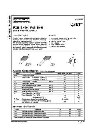
April 2000 TM QFET QFET QFET QFET FQB12N60 / FQI12N60 600V N-Channel MOSFET General Description Features These N-Channel enhancement mode power field effect 10.5A, 600V, RDS(on) = 0.7 @ VGS = 10 V transistors are produced using Fairchild s proprietary, Low gate charge ( typical 42 nC) planar stripe, DMOS technology. Low Crss ( typical 25 pF) This advanced technolo
fqa12n60.pdf
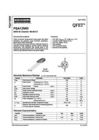
April 2000 TM QFET QFET QFET QFET FQA12N60 600V N-Channel MOSFET General Description Features These N-Channel enhancement mode power field effect 12A, 600V, RDS(on) = 0.7 @ VGS = 10 V transistors are produced using Fairchild s proprietary, Low gate charge ( typical 42 nC) planar stripe, DMOS technology. Low Crss ( typical 25 pF) This advanced technology has been e
hgtg12n60a4d hgtp12n60a4d hgt1s12n60a4d.pdf
HGTG12N60A4D, HGTP12N60A4D, HGT1S12N60A4DS Data Sheet December 2001 600V, SMPS Series N-Channel IGBT with Features Anti-Parallel Hyperfast Diode >100kHz Operation . . . . . . . . . . . . . . . . . . . . . 390V, 12A The HGTG12N60A4D, HGTP12N60A4D and 200kHz Operation . . . . . . . . . . . . . . . . . . . . . . . 390V, 9A HGT1S12N60A4DS are MOS gated high voltage switching
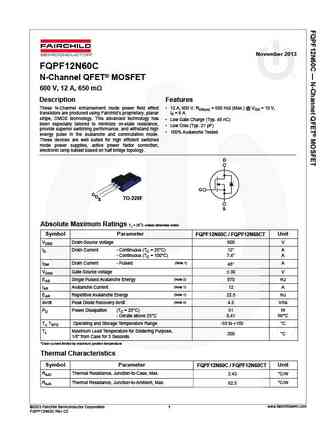
fqpf12n60.pdf

April 2000 TM QFET QFET QFET QFET FQPF12N60 600V N-Channel MOSFET General Description Features These N-Channel enhancement mode power field effect 5.8A, 600V, RDS(on) = 0.7 @ VGS = 10 V transistors are produced using Fairchild s proprietary, Low gate charge ( typical 42 nC) planar stripe, DMOS technology. Low Crss ( typical 25 pF) This advanced technology has been
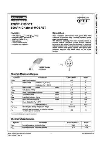
fqb12n60ctm fqi12n60ctu.pdf
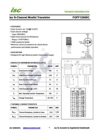
September 2007 QFET FQB12N60C / FQI12N60C 600V N-Channel MOSFET Features Description 12A, 600V, RDS(on) = 0.65 @VGS = 10 V These N-Channel enhancement mode power field effect Low gate charge ( typical 48 nC) transistors are produced using Fairchild s proprietary, planar stripe, DMOS technology. Low Crss ( typical 21pF) This advanced technology has been especially
fqaf12n60.pdf
April 2000 TM QFET QFET QFET QFET FQAF12N60 600V N-Channel MOSFET General Description Features These N-Channel enhancement mode power field effect 7.8A, 600V, RDS(on) = 0.7 @ VGS = 10 V transistors are produced using Fairchild s proprietary, Low gate charge ( typical 42 nC) planar stripe, DMOS technology. Low Crss ( typical 25 pF) This advanced technology has been
fqp12n60.pdf
April 2000 TM QFET QFET QFET QFET FQP12N60 600V N-Channel MOSFET General Description Features These N-Channel enhancement mode power field effect 10.5A, 600V, RDS(on) = 0.7 @ VGS = 10 V transistors are produced using Fairchild s proprietary, Low gate charge ( typical 42 nC) planar stripe, DMOS technology. Low Crss ( typical 25 pF) This advanced technology has been
fqp12n60c.pdf
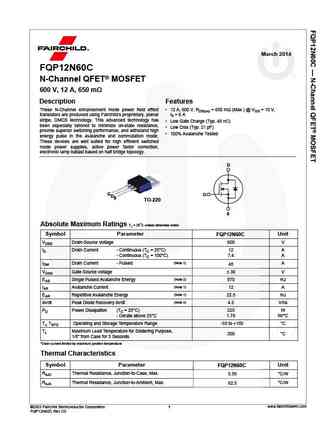
March 2014 FQP12N60C N-Channel QFET MOSFET 600 V, 12 A, 650 m Description Features These N-Channel enhancement mode power field effect 12 A, 600 V, RDS(on) = 650 m (Max.) @ VGS = 10 V, transistors are produced using Fairchild s proprietary, planar ID = 6 A stripe, DMOS technology. This advanced technology has Low Gate Charge (Typ. 48 nC) been especially tailored to
hgtg12n60a4 hgtp12n60a4 hgt1s12n60a4.pdf
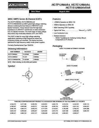
HGTP12N60A4, HGTG12N60A4, HGT1S12N60A4S9A Data Sheet August 2003 600V, SMPS Series N-Channel IGBTs Features The HGTP12N60A4, HGTG12N60A4 and >100kHz Operation at 390V, 12A HGT1S12N60A4S9A are MOS gated high voltage switching 200kHz Operation at 390V, 9A devices combining the best features of MOSFETs and 600V Switching SOA Capability bipolar transistors. These devices ha
hgtp12n60c3 hgt1s12n60c3.pdf
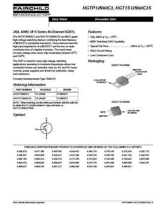
HGTP12N60C3, HGT1S12N60C3S Data Sheet December 2001 24A, 600V, UFS Series N-Channel IGBTs Features The HGTP12N60C3 and HGT1S12N60C3S are MOS gated 24A, 600V at TC = 25oC high voltage switching devices combining the best features 600V Switching SOA Capability of MOSFETs and bipolar transistors. These devices have the Typical Fall Time. . . . . . . . . . . . . . . . 230ns a
hgtg12n60c3d.pdf
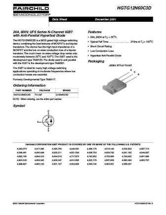
HGTG12N60C3D Data Sheet December 2001 24A, 600V, UFS Series N-Channel IGBT Features with Anti-Parallel Hyperfast Diode 24A, 600V at TC = 25oC The HGTG12N60C3D is a MOS gated high voltage switching Typical Fall Time. . . . . . . . . . . . . . . . 210ns at TJ = 150oC device combining the best features of MOSFETs and bipolar Short Circuit Rating transistors. The device has t
fdp12n60nz fdpf12n60nz.pdf
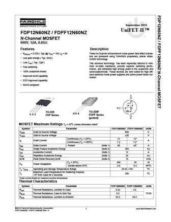
September 2010 UniFET-II TM FDP12N60NZ / FDPF12N60NZ N-Channel MOSFET 600V, 12A, 0.65 Features Description RDS(on) = 0.53 ( Typ.)@ VGS = 10V, ID = 6A These N-Channel enhancement mode power field effect transis- tors are produced using Fairchild s proprietary, planar stripe, Low gate charge ( Typ. 26nC) DOMS technology. Low Crss ( Typ. 12pF) This advance techno
fqpf12n60c.pdf

November 2013 FQPF12N60C N-Channel QFET MOSFET 600 V, 12 A, 650 m Description Features These N-Channel enhancement mode power field effect 12 A, 600 V, RDS(on) = 650 m (Max.) @ VGS = 10 V, transistors are produced using Fairchild s proprietary, planar ID = 6 A stripe, DMOS technology. This advanced technology has Low Gate Charge (Typ. 48 nC) been especially tailored
fqpf12n60ct.pdf
September 2006 QFET FQPF12N60CT 600V N-Channel MOSFET Features Description 12A, 600V, RDS(on) = 0.65 @VGS = 10 V These N-Channel enhancement mode power field effect Low gate charge ( typical 48 nC) transistors are produced using Fairchild s proprietary, planar stripe, DMOS technology. Low Crss ( typical 21 pF) This advanced technology has been especially tailored
fqp12n60c fqpf12n60c.pdf
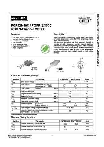
September 2007 QFET FQP12N60C / FQPF12N60C 600V N-Channel MOSFET Features Description 12A, 600V, RDS(on) = 0.65 @VGS = 10 V These N-Channel enhancement mode power field effect Low gate charge ( typical 48 nC) transistors are produced using Fairchild s proprietary, planar stripe, DMOS technology. Low Crss ( typical 21pF) This advanced technology has been especiall
hgtp12n60c3d hgt1s12n60c3d.pdf
HGTP12N60C3D, HGT1S12N60C3DS Data Sheet December 2001 24A, 600V, UFS Series N-Channel IGBT Features with Anti-Parallel Hyperfast Diodes 24A, 600V at TC = 25oC This family of MOS gated high voltage switching devices Typical Fall Time at TJ = 150oC . . . . . . . . . . . . . . . . 210ns combine the best features of MOSFETs and bipolar Short Circuit Rating transistors. The
fqpf12n60 fqpf12n60t.pdf
April 2000 TM QFET QFET QFET QFET FQPF12N60 600V N-Channel MOSFET General Description Features These N-Channel enhancement mode power field effect 5.8A, 600V, RDS(on) = 0.7 @ VGS = 10 V transistors are produced using Fairchild s proprietary, Low gate charge ( typical 42 nC) planar stripe, DMOS technology. Low Crss ( typical 25 pF) This advanced technology has been
siha12n60e.pdf
SiHA12N60E www.vishay.com Vishay Siliconix E Series Power MOSFET FEATURES PRODUCT SUMMARY Low figure-of-merit (FOM) Ron x Qg VDS (V) at TJ max. 650 Low input capacitance (Ciss) RDS(on) max. at 25 C ( ) VGS = 10 V 0.38 Reduced switching and conduction losses Qg max. (nC) 58 Ultra low gate charge (Qg) Qgs (nC) 6 Avalanche energy rated (UIS) Qgd (nC) 13 M
sihp12n60e.pdf
SiHP12N60E www.vishay.com Vishay Siliconix E Series Power MOSFET FEATURES PRODUCT SUMMARY Low Figure-of-Merit (FOM) Ron x Qg VDS (V) at TJ max. 650 Low Input Capacitance (Ciss) RDS(on) max. at 25 C ( ) VGS = 10 V 0.38 Reduced Switching and Conduction Losses Qg max. (nC) 58 Ultra Low Gate Charge (Qg) Qgs (nC) 6 Avalanche Energy Rated (UIS) Qgd (nC) 13
sihf12n60e.pdf
SiHF12N60E www.vishay.com Vishay Siliconix E Series Power MOSFET FEATURES PRODUCT SUMMARY Low Figure-of-Merit (FOM) Ron x Qg VDS (V) at TJ max. 650 Low Input Capacitance (Ciss) RDS(on) max. at 25 C ( ) VGS = 10 V 0.38 Reduced Switching and Conduction Losses Qg max. (nC) 58 Ultra Low Gate Charge (Qg) Qgs (nC) 6 Avalanche Energy Rated (UIS) Qgd (nC) 13
sihb12n60e.pdf
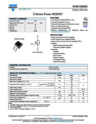
SiHB12N60E www.vishay.com Vishay Siliconix E Series Power MOSFET FEATURES PRODUCT SUMMARY Low Figure-of-Merit (FOM) Ron x Qg VDS (V) at TJ max. 650 Low Input Capacitance (Ciss) RDS(on) max. at 25 C ( ) VGS = 10 V 0.38 Reduced Switching and Conduction Losses Qg max. (nC) 58 Ultra Low Gate Charge (Qg) Qgs (nC) 6 Avalanche Energy Rated (UIS) Qgd (nC) 13
ixga12n60cd1 ixgp12n60cd1.pdf
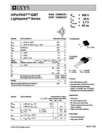
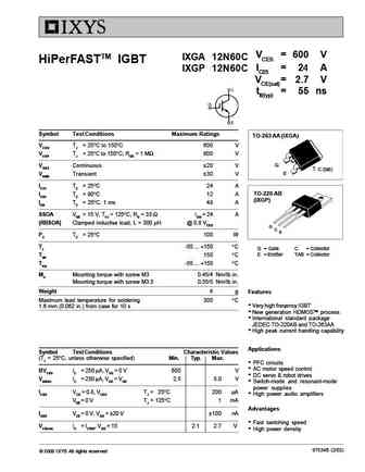
IXGA 12N60CD1 HiPerFASTTM IGBT VCES = 600 V IXGP 12N60CD1 LightspeedTM Series IC25 = 24 A VCE(sat) = 2.7 V tfi(typ) = 55 ns Symbol Test Conditions Maximum Ratings TO-263 (IXGA) VCES TJ = 25 C to 150 C 600 V G VCGR TJ = 25 C to 150 C; RGE = 1 M 600 V E C (TAB) VGES Continuous 20 V VGEM Transient 30 V IC25 TC = 25 C24 A IC90 TC = 90 C12 A TO-220 AB ICM TC = 25 C,
ixga12n60b ixgp12n60b.pdf

IXGA 12N60B VCES = 600 V HiPerFASTTM IGBT IXGP 12N60B IC25 = 24 A VCE(sat) = 2.1 V tfi(typ) = 120 ns Preliminary data sheet Symbol Test Conditions Maximum Ratings TO-220 AB (IXGP) VCES TJ = 25 C to 150 C 600 V VCGR TJ = 25 C to 150 C; RGE = 1 M 600 V C (TAB) VGES Continuous 20 V G E VGEM Transient 30 V IC25 TC = 25 C24 A IC90 TC = 90 C12 A TO-263 AA (IXGA) ICM TC =
ixgp12n60c.pdf

VCES = 600 V IXGA 12N60C HiPerFASTTM IGBT IC25 = 24 A IXGP 12N60C VCE(sat)= 2.7 V tfi(typ) = 55 ns Symbol Test Conditions Maximum Ratings TO-263 AA (IXGA) VCES TJ = 25 C to 150 C 600 V VCGR TJ = 25 C to 150 C; RGE = 1 M 600 V G VGES Continuous 20 V C (tab) E VGEM Transient 30 V IC25 TC = 25 C24 A TO-220 AB IC90 TC = 90 C12 A (IXGP) ICM TC = 25 C, 1 ms 48
ixgp12n60cd1.pdf

IXGA 12N60CD1 HiPerFASTTM IGBT VCES = 600 V IXGP 12N60CD1 LightspeedTM Series IC25 = 24 A VCE(sat) = 2.7 V tfi(typ) = 55 ns Symbol Test Conditions Maximum Ratings TO-263 (IXGA) VCES TJ = 25 C to 150 C 600 V G VCGR TJ = 25 C to 150 C; RGE = 1 M 600 V E C (TAB) VGES Continuous 20 V VGEM Transient 30 V IC25 TC = 25 C24 A IC90 TC = 90 C12 A TO-220 AB ICM TC = 25 C,
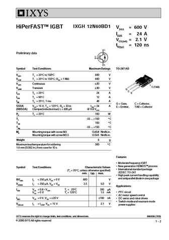
ixgh12n60cd1.pdf
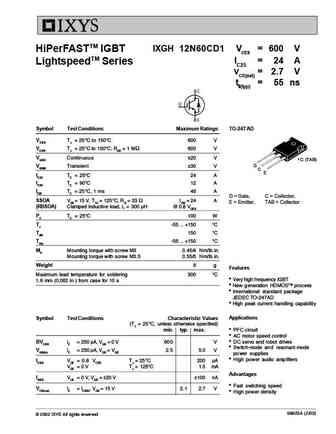
HiPerFASTTM IGBT IXGH 12N60CD1 VCES = 600 V IC25 = 24 A LightspeedTM Series VCE(sat) = 2.7 V tfi(typ) = 55 ns Symbol Test Conditions Maximum Ratings TO-247 AD VCES TJ = 25 C to 150 C 600 V VCGR TJ = 25 C to 150 C; RGE = 1 M 600 V VGES Continuous 20 V C (TAB) G VGEM Transient 30 V C E IC25 TC = 25 C24 A IC90 TC = 90 C12 A ICM TC = 25 C, 1 ms 48 A G = Gate, C = Co
ixgr12n60c.pdf
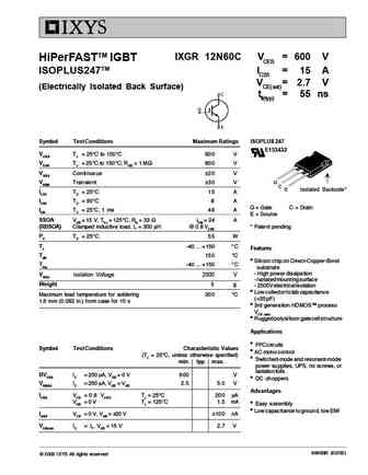
IXGR 12N60C VCES = 600 V HiPerFASTTM IGBT IC25 = 15 A ISOPLUS247TM VCE(sat)= 2.7 V (Electrically Isolated Back Surface) tfi(typ) = 55 ns Symbol Test Conditions Maximum Ratings ISOPLUS 247 E153432 VCES TJ = 25 C to 150 C 600 V VCGR TJ = 25 C to 150 C; RGE = 1 M 600 V VGES Continuous 20 V VGEM Transient 30 V G C E Isolated Backside* IC25 TC = 25 C15 A IC90 TC = 90 C
ixga12n60c ixgp12n60c.pdf
VCES = 600 V IXGA 12N60C HiPerFASTTM IGBT IC25 = 24 A IXGP 12N60C VCE(sat)= 2.7 V tfi(typ) = 55 ns Symbol Test Conditions Maximum Ratings TO-263 AA (IXGA) VCES TJ = 25 C to 150 C 600 V VCGR TJ = 25 C to 150 C; RGE = 1 M 600 V G VGES Continuous 20 V C (tab) E VGEM Transient 30 V IC25 TC = 25 C24 A TO-220 AB IC90 TC = 90 C12 A (IXGP) ICM TC = 25 C, 1 ms 48
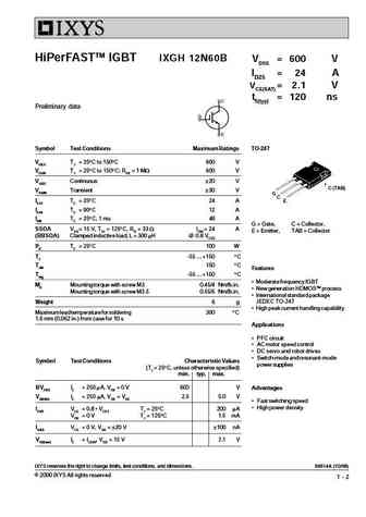
ixgh12n60c.pdf
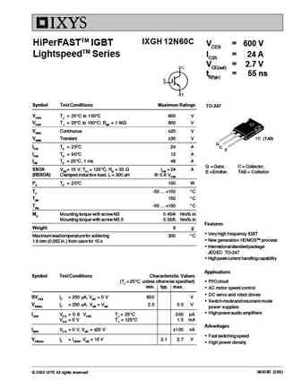
IXGH 12N60C HiPerFASTTM IGBT VCES = 600 V LightspeedTM Series IC25 = 24 A VCE(sat) = 2.7 V tfi(typ) = 55 ns Symbol Test Conditions Maximum Ratings TO-247 VCES TJ = 25 C to 150 C 600 V VCGR TJ = 25 C to 150 C; RGE = 1 M 600 V VGES Continuous 20 V VGEM Transient 30 V C (TAB) G IC25 TC = 25 C24 A C E IC90 TC = 90 C12 A ICM TC = 25 C, 1 ms 48 A G = Gate, C = Collecto
ixgh12n60bd1.pdf
IXGH 12N60BD1 HiPerFASTTM IGBT VDSS = 600 V ID25 = 24 A VCE(sat) = 2.1 V tfi(typ) = 120 ns Preliminary data Symbol Test Conditions Maximum Ratings TO-247 AD VCES TJ = 25 C to 150 C 600 V VCGR TJ = 25 C to 150 C; RGE = 1 MW 600 V VGES Continuous 20 V C (TAB) VGEM Transient 30 V G C IC25 TC = 25 C24 A E IC90 TC = 90 C12 A ICM TC = 25 C, 1 ms 48 A G = Gate, C = Collect
ixgh12n60b.pdf
HiPerFASTTM IGBT IXGH 12N60B VDSS = 600 V ID25 = 24 A VCE(SAT) = 2.1 V tfi(typ) = 120 ns Preliminary data Symbol Test Conditions Maximum Ratings TO-247 VCES TJ = 25 C to 150 C 600 V VCGR TJ = 25 C to 150 C; RGE = 1 MW 600 V VGES Continuous 20 V C (TAB) VGEM Transient 30 V G C IC25 TC = 25 C24 A E IC90 TC = 90 C12 A ICM TC = 25 C, 1 ms 48 A G = Gate, C = Collector,
ixgp12n60b.pdf
IXGA 12N60B VCES = 600 V HiPerFASTTM IGBT IXGP 12N60B IC25 = 24 A VCE(sat) = 2.1 V tfi(typ) = 120 ns Preliminary data sheet Symbol Test Conditions Maximum Ratings TO-220 AB (IXGP) VCES TJ = 25 C to 150 C 600 V VCGR TJ = 25 C to 150 C; RGE = 1 M 600 V C (TAB) VGES Continuous 20 V G E VGEM Transient 30 V IC25 TC = 25 C24 A IC90 TC = 90 C12 A TO-263 AA (IXGA) ICM TC =
ixsa12n60au1.pdf
IXSA 12N60AU1 VCES = 600 V Low VCE(sat) IGBT IC25 = 24 A with Diode VCE(sat) = 2.5 V Short Circuit SOA Capability Preliminary data sheet Symbol Test Conditions Maximum Ratings TO-263AA VCES TJ = 25 C to 150 C 600 V VCGR TJ = 25 C to 150 C; RGE = 1 M 600 V G VGES Continuous 20 V E TAB VGEM Transient 30 V G = Gate, C = Collector, IC25 TC = 25 C24 A E = Emitter
fqp12n60c.pdf

Is Now Part of To learn more about ON Semiconductor, please visit our website at www.onsemi.com Please note As part of the Fairchild Semiconductor integration, some of the Fairchild orderable part numbers will need to change in order to meet ON Semiconductor s system requirements. Since the ON Semiconductor product management systems do not have the ability to manage part nomenclatur
hgtg12n60a4d hgtp12n60a4d hgt1s12n60a4ds.pdf
SMPS Series N-Channel IGBT with Anti-Parallel Hyperfast Diode 600 V HGTG12N60A4D, www.onsemi.com HGTP12N60A4D, HGT1S12N60A4DS C The HGTG12N60A4D, HGTP12N60A4D and HGT1S12N60A4DS are MOS gated high voltage switching devices G combining the best features of MOSFETs and bipolar transistors. These devices have the high input impedance of a MOSFET and the E low on-state conduction los
hgtg12n60c3d.pdf
UFS Series N-Channel IGBT with Anti-Parallel Hyperfast Diode 24 A, 600 V HGTG12N60C3D www.onsemi.com The HGTG12N60C3D is a MOS gated high voltage switching device combining the best features of MOSFETs and bipolar C transistors. The device has the high input impedance of a MOSFET and the low on-state conduction loss of a bipolar transistor. The much lower on-state voltage drop varies
fdp12n60nz fdpf12n60nz.pdf
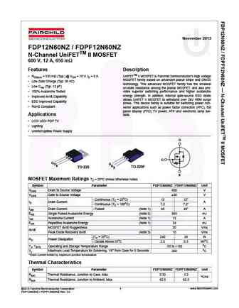
November 2013 FDP12N60NZ / FDPF12N60NZ N-Channel UniFETTM II MOSFET 600 V, 12 A, 650 m Features Description RDS(on) = 530 m (Typ.) @ VGS = 10 V, ID = 6 A UniFETTM II MOSFET is Fairchild Semiconductor s high voltage MOSFET family based on advanced planar stripe and DMOS Low Gate Charge (Typ. 26 nC) technology. This advanced MOSFET family has the smallest Low Crss (Typ.
fqpf12n60c.pdf
November 2013 FQPF12N60C N-Channel QFET MOSFET 600 V, 12 A, 650 m Description Features These N-Channel enhancement mode power field effect 12 A, 600 V, RDS(on) = 650 m (Max.) @ VGS = 10 V, transistors are produced using Fairchild s proprietary, planar ID = 6 A stripe, DMOS technology. This advanced technology has Low Gate Charge (Typ. 48 nC) been especially tailored
hgtp12n60c3d hgt1s12n60c3ds.pdf

Is Now Part of To learn more about ON Semiconductor, please visit our website at www.onsemi.com Please note As part of the Fairchild Semiconductor integration, some of the Fairchild orderable part numbers will need to change in order to meet ON Semiconductor s system requirements. Since the ON Semiconductor product management systems do not have the ability to manage part nomenclatur
12n60.pdf
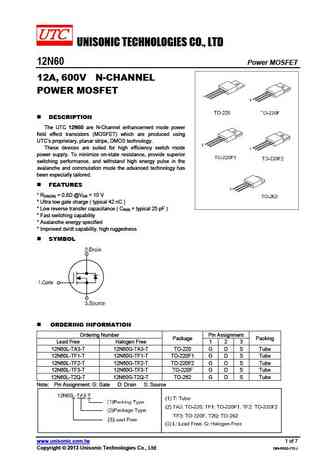
UNISONIC TECHNOLOGIES CO., LTD 12N60 Power MOSFET 12A, 600V N-CHANNEL POWER MOSFET DESCRIPTION The UTC 12N60 are N-Channel enhancement mode power field effect transistors (MOSFET) which are produced using UTC s proprietary, planar stripe, DMOS technology. These devices are suited for high efficiency switch mode power supply. To minimize on-state resistance, provide superi
fmi12n60es.pdf
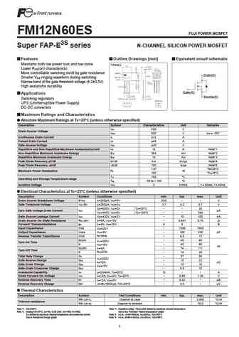
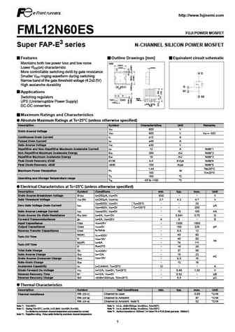
FMI12N60ES FUJI POWER MOSFET Super FAP-E3S series N-CHANNEL SILICON POWER MOSFET Features Outline Drawings [mm] Equivalent circuit schematic Maintains both low power loss and low noise T-Pack(L) Lower R (on) characteristic DS More controllable switching dv/dt by gate resistance Drain(D) Smaller V ringing waveform during switching GS Narrow band of the gate threshold voltage (4.2 0.5
fml12n60es.pdf
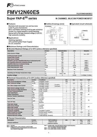
http //www.fujisemi.com FML12N60ES FUJI POWER MOSFET Super FAP-E3 series N-CHANNEL SILICON POWER MOSFET Features Outline Drawings [mm] Equivalent circuit schematic Maintains both low power loss and low noise TFP 9.0 0.2 7.0 0.2 0.4 0.1 Lower R (on) characteristic DS 4 More controllable switching dv/dt by gate resistance 4 D Smaller V ringing waveform during switching GS Narrow
fmv12n60es.pdf
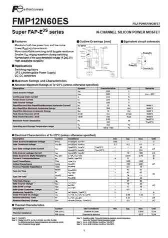
FMV12N60ES FUJI POWER MOSFET Super FAP-E3S series N-CHANNEL SILICON POWER MOSFET Features Outline Drawings [mm] Equivalent circuit schematic Maintains both low power loss and low noise TO-220F(SLS) Lower R (on) characteristic DS More controllable switching dv/dt by gate resistance Drain(D) Smaller V ringing waveform during switching GS Narrow band of the gate threshold voltage (4.2
fmc12n60es.pdf

FMC12N60ES FUJI POWER MOSFET Super FAP-E3S series N-CHANNEL SILICON POWER MOSFET Features Outline Drawings [mm] Equivalent circuit schematic Maintains both low power loss and low noise T-Pack(S) Lower R (on) characteristic DS More controllable switching dv/dt by gate resistance Drain(D) Smaller V ringing waveform during switching GS Narrow band of the gate threshold voltage (4.2 0.5
fmp12n60es.pdf
FMP12N60ES FUJI POWER MOSFET Super FAP-E3S series N-CHANNEL SILICON POWER MOSFET Features Outline Drawings [mm] Equivalent circuit schematic Maintains both low power loss and low noise TO-220AB Lower R (on) characteristic DS More controllable switching dv/dt by gate resistance Drain(D) Smaller V ringing waveform during switching GS Narrow band of the gate threshold voltage (4.2 0.5V
hgtp12n60c3.pdf
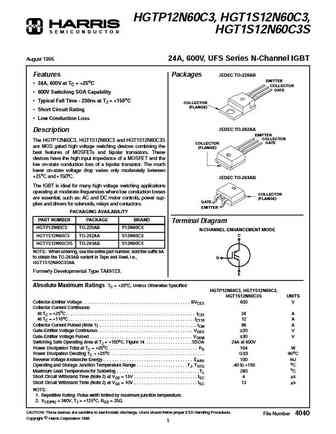
HGTP12N60C3, HGT1S12N60C3, S E M I C O N D U C T O R HGT1S12N60C3S August 1995 24A, 600V, UFS Series N-Channel IGBT Features Packages JEDEC TO-220AB EMITTER 24A, 600V at TC = +25oC COLLECTOR GATE 600V Switching SOA Capability Typical Fall Time - 230ns at TJ = +150oC COLLECTOR (FLANGE) Short Circuit Rating Low Conduction Loss JEDEC TO-262AA Description EMITTER
hgtg12n60d1d.pdf
S E M I C O N D U C T O R HGTG12N60D1D 12A, 600V N-Channel IGBT with Anti-Parallel Ultrafast Diode April 1995 Features Package JEDEC STYLE TO-247 12A, 600V Latch Free Operation EMITTER COLLECTOR Typical Fall Time
hgtg12n60c3d .pdf
S E M I C O N D U C T O R HGTG12N60C3D 24A, 600V, UFS Series N-Channel IGBT with Anti-Parallel Hyperfast Diode January 1997 Features Package 24A, 600V at TC = 25oC JEDEC STYLE TO-247 Typical Fall Time . . . . . . . . . . . . . . 210ns at TJ = 150oC E C Short Circuit Rating G Low Conduction Loss Hyperfast Anti-Parallel Diode Description The HGTG12N60C3D is a MO
hgtg12n60c3d.pdf
S E M I C O N D U C T O R HGTG12N60C3D 24A, 600V, UFS Series N-Channel IGBT with Anti-Parallel Hyperfast Diode August 1995 Features Package 24A, 600V at TC = +25oC JEDEC STYLE TO-247 Typical Fall Time - 210ns at TJ = +150oC E C Short Circuit Rating G Low Conduction Loss Hyperfast Anti-Parallel Diode Description The HGTG12N60C3D is a MOS gated high voltage swit
cjp12n60.pdf
JIANGSU CHANGJIANG ELECTRONICS TECHNOLOGY CO., LTD TO-220-3L Plastic-Encapsulate MOSFETS CJP12N60 600V N-Channel Power MOSFET TO-220-3L General Description This advanced technology has been especially tailored to minimize on-state resistance, provide superior switching performance, and withistand 1. GATE high energy pulse in the avalanche and commutation mode. These devices
cjpf12n60.pdf
JIANGSU CHANGJIANG ELECTRONICS TECHNOLOGY CO., LTD TO-220 / F Plastic-Encapsulate MOSFETS CJP12N60,CJPF12N60 600V N-Channel Power MOSFET General Description This advanced technology has been especially tailored to minimize on-state resistance, provide superior switching performance, and withistand high energy pulse in the avalanche and commutation mode. T
kf12n60p-f.pdf
KF12N60P/F SEMICONDUCTOR N CHANNEL MOS FIELD TECHNICAL DATA EFFECT TRANSISTOR General Description KF12N60P This planar stripe MOSFET has better characteristics, such as fast switching time, low on resistance, low gate charge and excellent avalanche characteristics. It is mainly suitable for active power factor correction and switching mode power supplies. FEATURES VDSS=600V, ID=
kf12n60p kf12n60f.pdf
KF12N60P/F SEMICONDUCTOR N CHANNEL MOS FIELD TECHNICAL DATA EFFECT TRANSISTOR General Description KF12N60P A This planar stripe MOSFET has better characteristics, such as fast O C switching time, low on resistance, low gate charge and excellent F avalanche characteristics. It is mainly suitable for active power factor E DIM MILLIMETERS G _ + correction and switching mode power
h12n60.pdf
Spec. No. MOS200902 HI-SINCERITY Issued Date 2009.01.20 Revised Date MICROELECTRONICS CORP. Page No. 1/4 H12N60F H12N60F N-Channel Power MOSFET (600V,12A) 3-Lead TO-220FP) Plastic Package Package Code F Applications Pin 1 Gate Switch Mode Power Supply Pin 2 Drain Pin 3 Source Uninterruptable Power Supply 3 2 1 High Speed Power Switch
aow12n60 aowf12n60.pdf
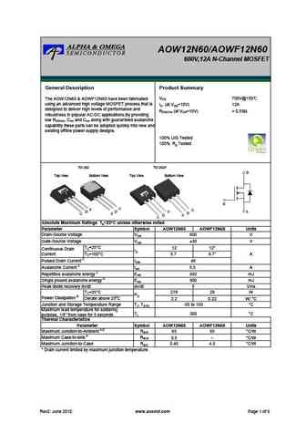
AOW12N60/AOWF12N60 600V,12A N-Channel MOSFET General Description Product Summary VDS 700V@150 The AOW12N60 & AOWF12N60 have been fabricated using an advanced high voltage MOSFET process that is ID (at VGS=10V) 12A designed to deliver high levels of performance and RDS(ON) (at VGS=10V)
aowf12n60.pdf
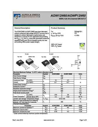
AOW12N60/AOWF12N60 600V,12A N-Channel MOSFET General Description Product Summary VDS The AOW12N60 & AOWF12N60 have been fabricated 700V@150 12A using an advanced high voltage MOSFET process that is ID (at VGS=10V) designed to deliver high levels of performance and
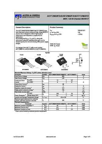
aot12n60.pdf

AOT12N60/AOTF12N60 600V,12A N-Channel MOSFET General Description Product Summary VDS 700V@150 The AOT12N60 & AOTF12N60 have been fabricated using an advanced high voltage MOSFET process that is ID (at VGS=10V) 12A designed to deliver high levels of performance and RDS(ON) (at VGS=10V)
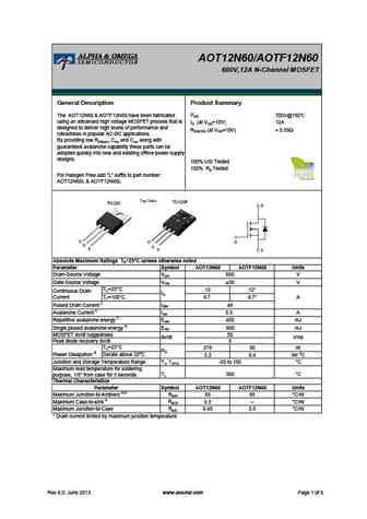
aotf12n60.pdf

AOT12N60/AOTF12N60 600V,12A N-Channel MOSFET General Description Product Summary VDS 700V@150 The AOT12N60 & AOTF12N60 have been fabricated using an advanced high voltage MOSFET process that is ID (at VGS=10V) 12A designed to deliver high levels of performance and RDS(ON) (at VGS=10V)
aot12n60fd.pdf

AOT12N60FD/AOB12N60FD/AOTF12N60FD 600V, 12A N-Channel MOSFET General Description Product Summary VDS 700V@150 The AOT12N60FD/AOB12N60FD/AOTF12N60FD have been fabricated using an advanced high voltage MOSFET ID (at VGS=10V) 12A process that is designed to deliver high levels of RDS(ON) (at VGS=10V)
aotf12n60fd.pdf
AOT12N60FD/AOB12N60FD/AOTF12N60FD 600V, 12A N-Channel MOSFET General Description Product Summary VDS 700V@150 The AOT12N60FD/AOB12N60FD/AOTF12N60FD have been fabricated using an advanced high voltage MOSFET ID (at VGS=10V) 12A process that is designed to deliver high levels of RDS(ON) (at VGS=10V)
aob12n60fd.pdf

AOT12N60FD/AOB12N60FD/AOTF12N60FD 600V, 12A N-Channel MOSFET General Description Product Summary VDS 700V@150 The AOT12N60FD/AOB12N60FD/AOTF12N60FD have been fabricated using an advanced high voltage MOSFET ID (at VGS=10V) 12A process that is designed to deliver high levels of RDS(ON) (at VGS=10V)
aot12n60 aotf12n60.pdf
AOT12N60/AOTF12N60 600V,12A N-Channel MOSFET General Description Product Summary VDS 700V@150 The AOT12N60 & AOTF12N60 have been fabricated using an advanced high voltage MOSFET process that is ID (at VGS=10V) 12A designed to deliver high levels of performance and RDS(ON) (at VGS=10V)
aow12n60.pdf

AOW12N60/AOWF12N60 600V,12A N-Channel MOSFET General Description Product Summary VDS The AOW12N60 & AOWF12N60 have been fabricated 700V@150 12A using an advanced high voltage MOSFET process that is ID (at VGS=10V) designed to deliver high levels of performance and
afn12n60t220ft afn12n60t220t.pdf
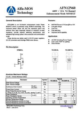
AFN12N60 Alfa-MOS 600V / 12A N-Channel Technology Enhancement Mode MOSFET General Description Features AFN12N60 is an N-channel enhancement mode Power 600V/6A,RDS(ON)=0.75 (MAX)@VGS=10V MOSFET which is produced using VDMOS technology. The Low gate charge improved planar stripe cell and the improved guard ring Low Crss terminal have been especially tailored to minimize on-sta
sss12n60.pdf
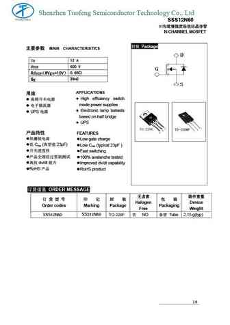
Shenzhen Tuofeng Semiconductor Technology Co., Ltd SSS12N60 N N-CHANNEL MOSFET Package MAIN CHARACTERISTICS 12 A ID 600 V VDSS Rdson 0.65 @Vgs=10V 39nC Qg APPLICATIONS High efficiency switch mode power supplies Electronic lamp ballasts UPS
sif12n60c.pdf
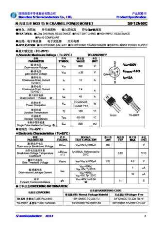
Shenzhen SI Semiconductors Co., LTD. Product Specification Shenzhen SI Semiconductors Co., LTD. Product Specification Shenzhen SI Semiconductors Co., LTD. Product Specification Shenzhen SI Semiconductors Co., LTD. Product Specification N- MOS / N-CHANNEL POWER MOSFET SIF12N60C N- MOS / N-CHANNEL POWER MOSFET SIF12N60C
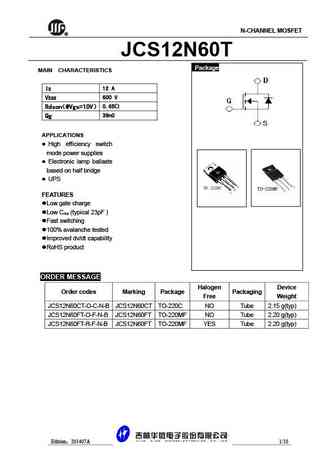
jcs12n60ct jcs12n60ft jcs12n60st jcs12n60bt.pdf
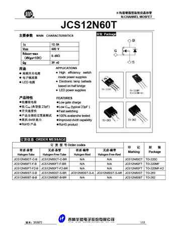
N R N-CHANNEL MOSFET JCS12N60T Package MAIN CHARACTERISTICS ID 12.0A VDSS 600 V Rdson-max 0.65 @Vgs=10V Qg 39 nC APPLICATIONS High efficiency switch mode power supplies Electronic lamp ballasts LED based on half bridge L
mtn12n60fp.pdf
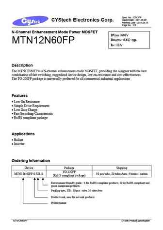
Spec. No. C743FP Issued Date 2011.05.09 CYStech Electronics Corp. Revised Date 2014.05.15 Page No. 1/9 N-Channel Enhancement Mode Power MOSFET BVDSS 600V RDS(ON) 0.6 typ. MTN12N60FP ID 12A Description The MTN12N60FP is a N-channel enhancement-mode MOSFET, providing the designer with the best combination of fast switching, ruggedized device design, low on-re
mtn12n60e3.pdf
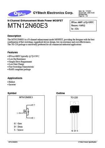
Spec. No. C743E3 Issued Date 2009.10.08 CYStech Electronics Corp. Revised Date Page No. 1/8 N-Channel Enhancement Mode Power MOSFET BVDSS 660V @Tj=150 C RDS(ON) 0.65 MTN12N60E3 ID 12A Description The MTN12N60E3 is a N-channel enhancement-mode MOSFET, providing the designer with the best combination of fast switching, ruggedized device design, low on-resist
mtn12n60bfp.pdf
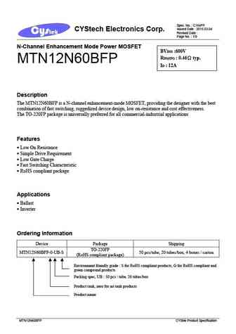
Spec. No. C164FP Issued Date 2015.03.04 CYStech Electronics Corp. Revised Date Page No. 1/9 N-Channel Enhancement Mode Power MOSFET BVDSS 600V RDS(ON) 0.46 typ. MTN12N60BFP ID 12A Description The MTN12N60BFP is a N-channel enhancement-mode MOSFET, providing the designer with the best combination of fast switching, ruggedized device design, low on-resistanc
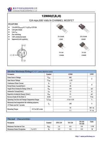
12n60 12n60f.pdf
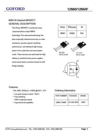
GOFORD 12N60/12N60F 600V N-Channel MOSFET GENERAL DESCRIPTION VDSS RDS(ON) ID This Power MOSFET is produced using advanced planar stripe DMOS 600V 0.65 12A technology.This advanced technology has been especially tailored tominimize on-state resistance, provide superior switching performance, and withstand high energy pulse in the avalanche and commutation mode. These devices are
ssf12n60f.pdf
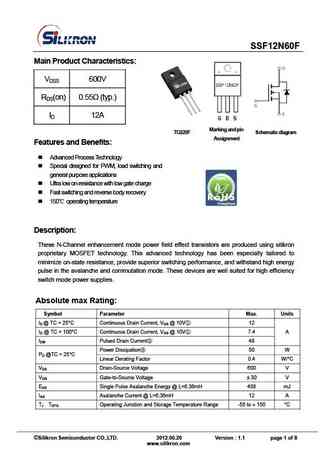
SSF12N60F Main Product Characteristics VDSS 600V RDS(on) 0.55 (typ.) ID 12A Sche ma ti c di agr a m TO220F Marking and pin Assignment Features and Benefits Advanced Process Technology Special designed for PWM, load switching and general purpose applications Ultra low on-resistance with low gate charge Fast switching and reverse body recovery
12n60a 12n60af.pdf
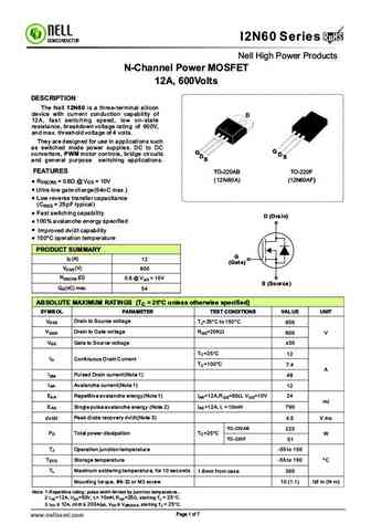
RoHS I2N60 Series RoHS SEMICONDUCTOR Nell High Power Products N-Channel Power MOSFET 12A, 600Volts DESCRIPTION The Nell 12N60 is a three-terminal silicon device with current conduction capability of D 12A, fast switching speed, low on-state resistance, breakdown voltage rating of 600V, and max. threshold voltage of 4 volts. They are designed for use in applications such as s
hfh12n60.pdf
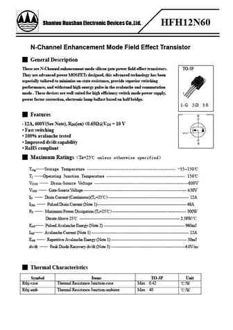
Shantou Huashan Electronic Devices Co.,Ltd. HFH12N60 N-Channel Enhancement Mode Field Effect Transistor General Description These are N-Channel enhancement mode silicon gate power field effect transistors. TO-3P They are advanced power MOSFETs designed, this advanced technology has been especially tailored to minimize on-state resistance, provide superior switching performanc
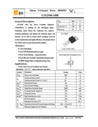
cs12n60 a8r.pdf
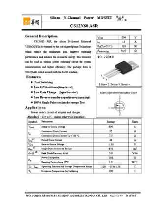
Silicon N-Channel Power MOSFET R CS12N60 A8R General Description VDSS 600 V CS12N60 A8R, the silicon N-channel Enhanced ID 12 A PD(TC=25 ) 150 W VDMOSFETs, is obtained by the self-aligned planar Technology RDS(ON)Typ 0.57 which reduce the conduction loss, improve switching performance and enhance the avalanche energy. The transistor can be used in various po
cs12n60f a9r.pdf

Silicon N-Channel Power MOSFET R CS12N60F A9R General Description VDSS 600 V CS12N60F A9R, the silicon N-channel Enhanced ID 12 A PD(TC=25 ) 42 W VDMOSFETs, is obtained by the self-aligned planar Technology RDS(ON)Typ 0.57 which reduce the conduction loss, improve switching performance and enhance the avalanche energy. The transistor can be used in various p
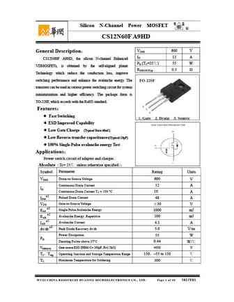
cs12n60f a9hd.pdf

Silicon N-Channel Power MOSFET R CS12N60F A9HD VDSS 600 V General Description ID 12 A CS12N60F A9HD, the silicon N-channel Enhanced PD (TC=25 ) 55 W VDMOSFETs, is obtained by the self-aligned planar RDS(ON)Typ 0.5 Technology which reduce the conduction loss, improve switching performance and enhance the avalanche energy. The transistor can be used in vario
cs12n60 a8h.pdf
Silicon N-Channel Power MOSFET R CS12N60 A8H VDSS 600 V General Description ID 12 A CS12N60 A8H, the silicon N-channel Enhanced PD (TC=25 ) 140 W VDMOSFETs, is obtained by the self-aligned planar RDS(ON)Typ 0.5 Technology which reduce the conduction loss, improve switching performance and enhance the avalanche energy. The transistor can be used in various po
cs12n60 a8hd.pdf

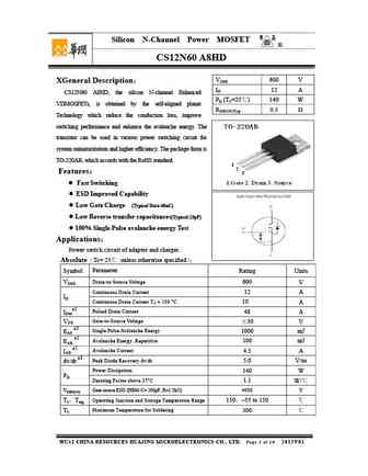
Silicon N-Channel Power MOSFET R CS12N60 A8HD VDSS 600 V XGeneral Description ID 12 A CS12N60 A8HD, the silicon N-channel Enhanced PD (TC=25 ) 140 W VDMOSFETs, is obtained by the self-aligned planar RDS(ON)Typ 0.5 Technology which reduce the conduction loss, improve switching performance and enhance the avalanche energy. The transistor can be used in various
cs12n60f a9h.pdf
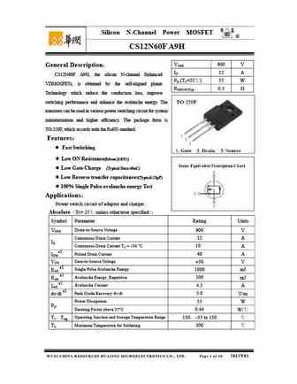
Silicon N-Channel Power MOSFET R CS12N60F A9H VDSS 600 V General Description ID 12 A CS12N60F A9H, the silicon N-channel Enhanced PD (TC=25 ) 55 W VDMOSFETs, is obtained by the self-aligned planar RDS(ON)Typ 0.5 Technology which reduce the conduction loss, improve switching performance and enhance the avalanche energy. The transistor can be used in various
cm12n60a to220a.pdf
R CM12N60A www.jdsemi.cn ShenZhen Jingdao Electronic Co.,Ltd. POWER MOSFET 600V N-Channel VDMOS RoHS 1 LD E 2 3
cm12n60af.pdf
R CM12N60AF www.jdsemi.cn ShenZhen Jingdao Electronic Co.,Ltd. POWER MOSFET 600V N-Channel VDMOS RoHS 1 LD E 2 1
f12n60.pdf
F12N60 12A 600V N-channel Enhancement Mode Power MOSFET 1 Description These N-channel enhanced vdmosfets, is obtained by the self-aligned V DSS = 600V planar technology which reduce the conduction loss, improve switching I = 12.0A D performance and enhance the avalanche energy. Which accords with the RoHS standard. TO-220F provides insulation voltage rated at 2000V R DS(on) TYP)
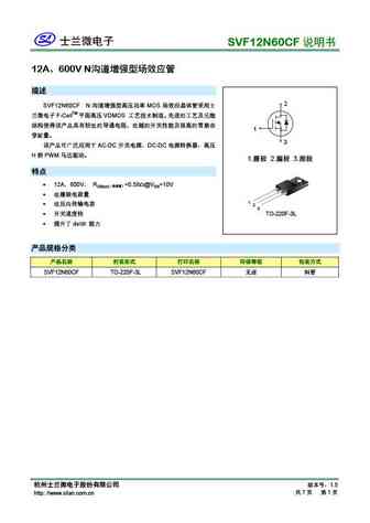
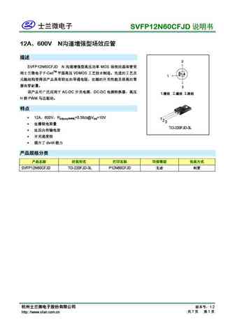
svf12n60cfj.pdf
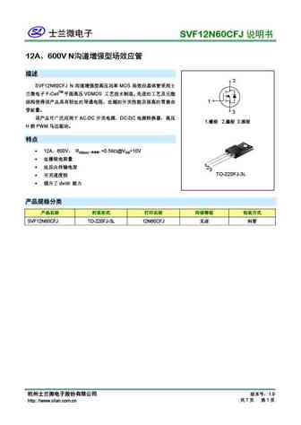
SVF12N60CFJ 12A 600V N 2 SVF12N60CFJ N MOS F-CellTM VDMOS 1 3
svf12n60f svf12n60s svf12n60str svf12n60k.pdf
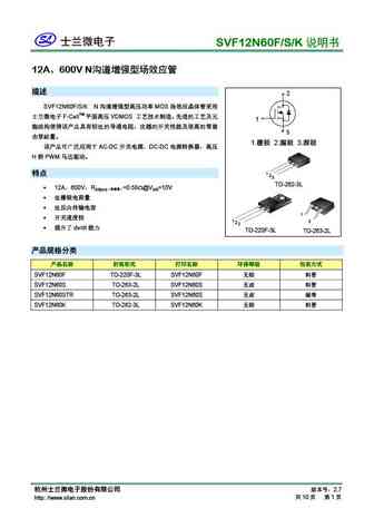
SVF12N60F/S/K 12A 600V N 2 SVF12N60F/S/K N MOS F-CellTM VDMOS 1 3 1. 2. 3
svf12n60t svf12n60f svf12n60s svf12n60k.pdf
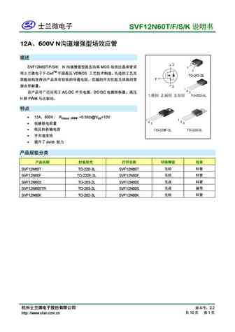
SVF12N60T/F/S/K 12A 600V N SVF12N60T/F/S/K N MOS F-CellTM VDMOS AC-DC
ms12n60.pdf
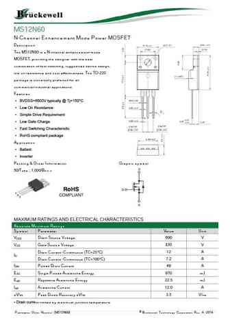
MS12N60 N-Channel Enhancement Mode Power MOSFET Description The MS12N60 is a N-channel enhancement-mode MOSFET, providing the designer with the best combination of fast switching, ruggedized device design, low on-resistance and cost effectiveness. The TO-220 package is universally preferred for all commercial-industrial applications Features BVDSS=6600V typically @ Tj=15
msf12n60.pdf
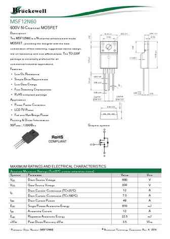
MSF12N60 600V N-Channel MOSFET Description The MSF12N60 is a N-channel enhancement-mode MOSFET , providing the designer with the best combination of fast switching, ruggedized device design, low on-resistance and cost effectiveness. The TO-220F package is universally preferred for all commercial-industrial applications Features Low On Resistance Simple Drive Requir
wff12n60.pdf
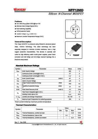
WFF12N60 WFF12N60 WFF12N60 WFF12N60 Silicon N-Channel MOSFET Silicon N-Channel MOSFET Silicon N-Channel MOSFET Silicon N-Channel MOSFET Features Features Features Features 12A, 600V,R (Max 0.65 )@V =10V DS(on) GS Ultra-low Gate Charge(Typical 39nC) Fast Switching Capability 100%Avalanche Tested Isolation Voltage ( V = 4000V AC ) ISO Maximum Junction T
wfp12n60.pdf
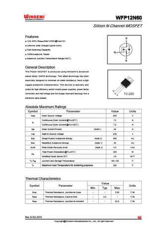
WFP12N60 WFP12N60 WFP12N60 WFP12N60 Silicon N-Channel MOSFET Features 12A, 600V,R (Max 0.65 )@V =10V DS(on) GS Ultra-low Gate Charge(Typical 43nC) Fast Switching Capability 100%Avalanche Tested Maximum Junction Temperature Range(150 ) General Description This Power MOSFET is produced using Winsemi s advanced planar stripe, DMOS technology. This latest tech
bl12n60-p bl12n60-a.pdf
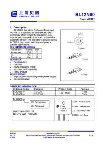
BL12N60 Power MOSFET Power MOSFET Power MOSFET Power MOSFET 1 Description BL12N60, the silicon N-channel Enhanced MOSFETs, is obtained by advanced MOSFET technology which reduce the conduction loss, improve switching performance and enhance the avalanche energy. The transistor is suitable device for SMPS, high speed switching and general purpose application
bl12n60a-p bl12n60a-a.pdf
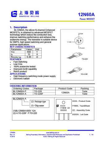
12N60A Power MOSFET 1 Description Step-Down Converter BL12N60A, the silicon N-channel Enhanced , MOSFETs, is obtained by advanced MOSFET technology which reduce the conduction loss, improve switching performance and enhance the avalanche energy. The transistor is suitable device for SMPS, high speed switching and general purpose applications. KEY CHARACTERISTICS Par
fhp12n60a fhf12n60a.pdf
N N-CHANNEL MOSFET FHP12N60A/ FHF12N60A MAIN CHARACTERISTICS FEATURES Low gate charge ID 12A Crss ( 18pF) Low Crss (typical 18pF ) VDSS 600V Fast switching Rdson-typ 0.6 @Vgs=10V 100% 100% avalanche tested Qg-typ 52nC dv/dt Im
jfpc12n60c jffm12n60c.pdf
JFPC12N60C JFFM12N60C 600V N-Channel MOSFET General Description Features This Power MOSFET is produced using advanced - 12A, 600V, RDS(on)typ. = 0.52 @VGS = 10 V planar stripe DMOS technology. This advanced - Low gate charge technology has been especially tailored to minimize - High ruggedness on-state resistance, provide superior switching - Fast switching performan
kia12n60h.pdf
12A 600V 12N60H N-CHANNELMOSFET KIA KIA KIA SEMICONDUCTORS SEMICONDUCTORS SEMICONDUCTORS 1.Description The KIA12N60H N-Channel enhancement mode silicon gate power MOSFET is designed for high voltage, high speed power switching applications such as high efficiency switched mode power supplies, active power factor correction, electronic lamp ballasts based on half bridge topology.
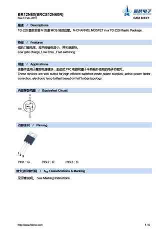
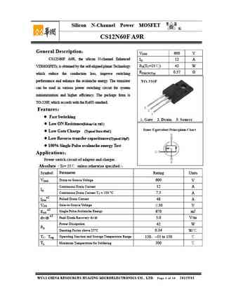
cs12n60.pdf
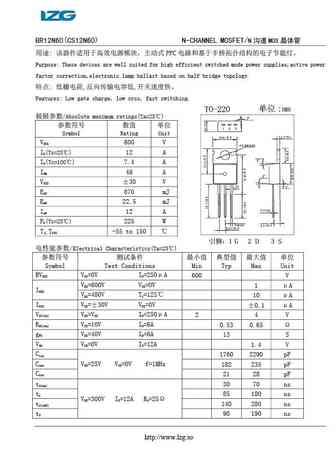
BR12N60(CS12N60) N-CHANNEL MOSFET/N MOS PFC Purpose These devices are well suited for high efficient switched mode power supplies,active power factor correction,electronic lamp ballast based on half bridge topology. , ,
slp12n60c slf12n60c.pdf
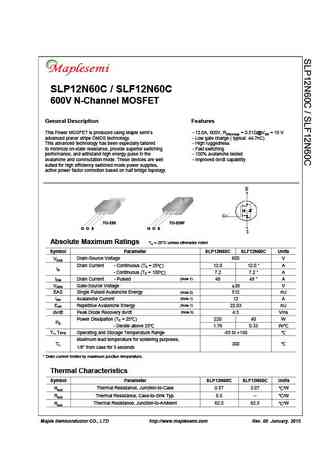
SLP12N60C / SLF12N60C 600V N-Channel MOSFET General Description Features This Power MOSFET is produced using Maple semi s - 12.0A, 600V, RDS(on)typ = 0.51 @VGS = 10 V advanced planar stripe DMOS technology. - Low gate charge ( typical 44.7nC) This advanced technology has been especially tailored - High ruggedness to minimize on-state resistance, provide superior switching - Fast switch
ptp12n60 pta12n60.pdf
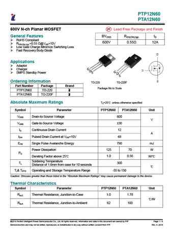
PTP12N60 PTA12N60 600V N-ch Planar MOSFET General Features BVDSS RDS(ON),typ. ID RoHS Compliant 600V 0.55 12A RDS(ON),typ.=0.55 @VGS=10V Low Gate Charge Minimize Switching Loss Fast Recovery Body Diode Applications Adaptor Charger G D S G D SMPS Standby Power S Ordering Information TO-220 TO-220F Part Number Package Brand
swf12n60d.pdf
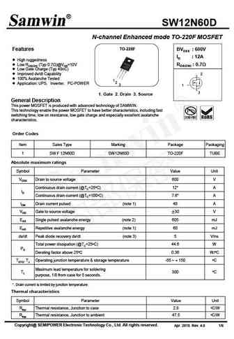
SW12N60D N-channel Enhanced mode TO-220F MOSFET TO-220F Features BVDSS 600V ID 12A High ruggedness Low RDS(ON) (Typ 0.7 )@VGS=10V RDS(ON) 0.7 Low Gate Charge (Typ 48nC) Improved dv/dt Capability 2 100% Avalanche Tested 1 2 Application UPS Inverter PC-POWER 3 1 3 1. Gate 2. Drain 3. Source General Description This power
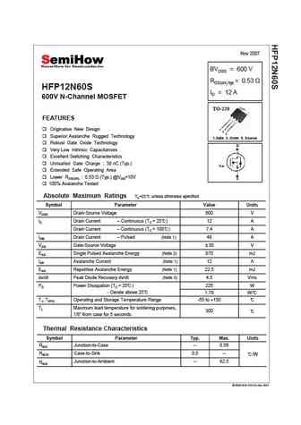
hfs12n60s.pdf
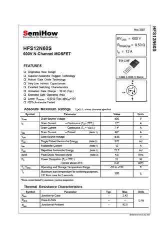
Nov 2007 BVDSS = 600 V RDS(on) typ = 0.53 HFS12N60S ID = 12 A 600V N-Channel MOSFET TO-220F FEATURES 1 Originative New Design 2 3 Superior Avalanche Rugged Technology 1.Gate 2. Drain 3. Source Robust Gate Oxide Technology Very Low Intrinsic Capacitances Excellent Switching Characteristics Unrivalled Gate Charge 38 nC (Typ.) Unrivalled Gate Charge 38 nC (Typ ) E
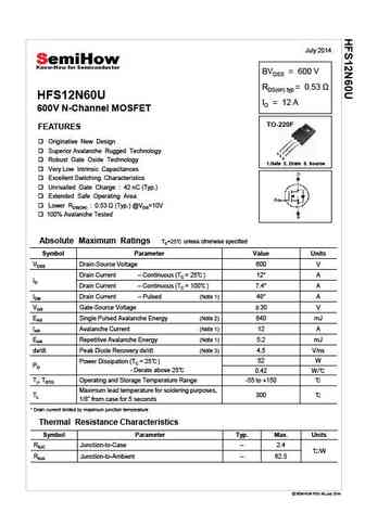
hfp12n60u.pdf
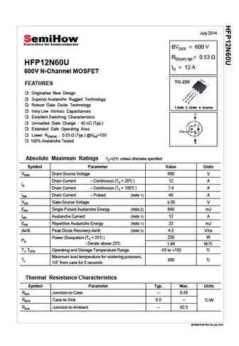
July 2014 BVDSS = 600 V RDS(on) typ = 0.53 HFP12N60U ID = 12 A 600V N-Channel MOSFET TO-220 FEATURES Originative New Design Superior Avalanche Rugged Technology 1 2 3 Robust Gate Oxide Technology 1.Gate 2. Drain 3. Source Very Low Intrinsic Capacitances Excellent Switching Characteristics Unrivalled Gate Charge 42 nC (Typ.) Extended Safe Operating Area Lo
hfp12n60s.pdf
Nov 2007 BVDSS = 600 V RDS(on) typ = 0.53 HFP12N60S ID = 12 A 600V N-Channel MOSFET TO-220 FEATURES Originative New Design 1 2 3 Superior Avalanche Rugged Technology 1.Gate 2. Drain 3. Source Robust Gate Oxide Technology Very Low Intrinsic Capacitances Excellent Switching Characteristics Unrivalled Gate Charge 38 nC (Typ.) Unrivalled Gate Charge 38 nC (Typ ) Ext
hfs12n60u.pdf
July 2014 BVDSS = 600 V RDS(on) typ = 0.53 HFS12N60U ID = 12 A 600V N-Channel MOSFET TO-220F FEATURES Originative New Design Superior Avalanche Rugged Technology 1 2 3 Robust Gate Oxide Technology 1.Gate 2. Drain 3. Source Very Low Intrinsic Capacitances Excellent Switching Characteristics Unrivalled Gate Charge 42 nC (Typ.) Extended Safe Operating Area Lo
hfw12n60s.pdf
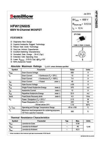
Jan 2013 BVDSS = 600 V RDS(on) typ = 0.53 HFW12N60S ID = 12 A 600V N-Channel MOSFET D2-PAK FEATURES Originative New Design Superior Avalanche Rugged Technology 1.Gate 2. Drain 3. Source Robust Gate Oxide Technology Very Low Intrinsic Capacitances Excellent Switching Characteristics Unrivalled Gate Charge 38 nC (Typ.) Extended Safe Operating Area Lower RDS(ON
sff12n60.pdf
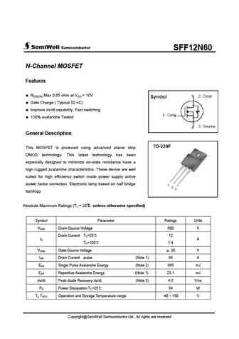
SemiWell Semiconductor SFF12N60 N-Channel MOSFET Features RDS(ON) Max 0.65 ohm at VGS = 10V Gate Charge ( Typical 52 nC) Improve dv/dt capability, Fast switching 100% avalanche Tested General Description This MOSFET is produced using advanced planar strip DMOS technology. This latest technology has been especially designed to minimize on-state resistance h
msu12n60f msu12n60t.pdf
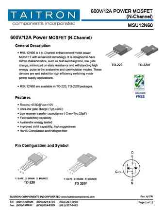
600V/12A POWER MOSFET (N-Channel) MSU12N60 600V/12A Power MOSFET (N-Channel) General Description MSU12N60 is a N-Channel enhancement mode power MOSFET with advanced technology. It is designed to have Better characteristics, such as fast switching time, low gate TO-220 TO-220F charge, minimized on-state resistance and withstanding high energy pulse in the avalanche and
tmp12n60a tmpf12n60a.pdf
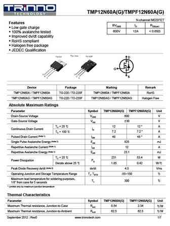
TMP12N60A(G)/TMPF12N60A(G) N-channel MOSFET Features BVDSS ID RDS(on) Low gate charge 600V 12A
tmp12n60 tmpf12n60.pdf
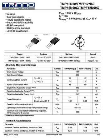
TMP12N60/TMPF12N60 TMP12N60G/TMPF12N60G VDSS = 660 V @Tjmax Features ID = 12A Low gate charge RDS(on) = 0.65 W(max) @ VGS= 10 V 100% avalanche tested Improved dv/dt capability RoHS compliant Halogen free package JEDEC Qualification D G S Device Package Marking Remark TMP12N60 / TMPF12N60 TO-220 / TO-220F TMP12N60 / TMPF12N60 RoHS TMP12N60G / TMPF12N60G
tsp12n60m tsf12n60m.pdf
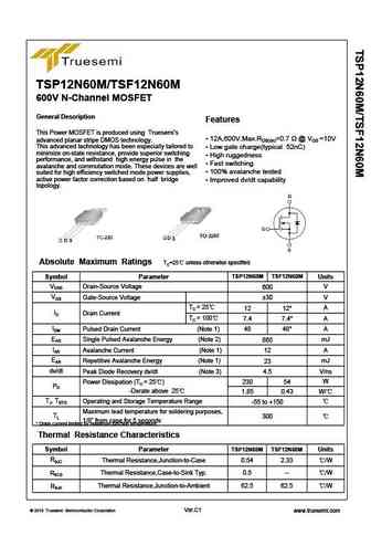
TSP12N60M/TSF12N60M 600V N-Channel MOSFET General Description Features This Power MOSFET is produced using Truesemi s 12A,600V,Max.RDS(on)=0.7 @ VGS =10V advanced planar stripe DMOS technology. This advanced technology has been especially tailored to Low gate charge(typical 52nC) minimize on-state resistance, provide superior switching High ruggedness performance, an
cs12n60fa9r.pdf
Silicon N-Channel Power MOSFET R CS12N60F A9R General Description VDSS 600 V CS12N60F A9R, the silicon N-channel Enhanced ID 12 A PD(TC=25 ) 42 W VDMOSFETs, is obtained by the self-aligned planar Technology RDS(ON)Typ 0.57 which reduce the conduction loss, improve switching performance and enhance the avalanche energy. The transistor can be used in various p
cs12n60a8hd.pdf
Silicon N-Channel Power MOSFET R CS12N60 A8HD VDSS 600 V XGeneral Description ID 12 A CS12N60 A8HD, the silicon N-channel Enhanced PD (TC=25 ) 140 W VDMOSFETs, is obtained by the self-aligned planar RDS(ON)Typ 0.5 Technology which reduce the conduction loss, improve switching performance and enhance the avalanche energy. The transistor can be used in various
cs12n60fa9h.pdf

Silicon N-Channel Power MOSFET R CS12N60F A9H VDSS 600 V General Description ID 12 A CS12N60F A9H, the silicon N-channel Enhanced PD (TC=25 ) 55 W VDMOSFETs, is obtained by the self-aligned planar RDS(ON)Typ 0.5 Technology which reduce the conduction loss, improve switching performance and enhance the avalanche energy. The transistor can be used in various
cs12n60fa9hd.pdf
Silicon N-Channel Power MOSFET R CS12N60F A9HD VDSS 600 V General Description ID 12 A CS12N60F A9HD, the silicon N-channel Enhanced PD (TC=25 ) 55 W VDMOSFETs, is obtained by the self-aligned planar RDS(ON)Typ 0.5 Technology which reduce the conduction loss, improve switching performance and enhance the avalanche energy. The transistor can be used in vario
cs12n60a8h.pdf

Silicon N-Channel Power MOSFET R CS12N60 A8H VDSS 600 V General Description ID 12 A CS12N60 A8H, the silicon N-channel Enhanced PD (TC=25 ) 140 W VDMOSFETs, is obtained by the self-aligned planar RDS(ON)Typ 0.5 Technology which reduce the conduction loss, improve switching performance and enhance the avalanche energy. The transistor can be used in various po
csfr12n60f.pdf
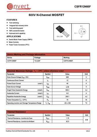
CSFR12N60F nvert Suzhou Convert Semiconductor Co ., Ltd. 600V N-Channel MOSFET FEATURES Fast switching Integrate fast recovery diode Fast switching speed 100% avalanche tested Improved dv/dt capability APPLICATIONS Switch Mode Power Supply (SMPS) Motor Controls Power Factor Correction (PFC) Device Marking and Package Information Device Package Mark
cs12n60f cs12n60p.pdf
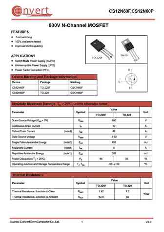
CS12N60F,CS12N60P nvert Suzhou Convert Semiconductor Co ., Ltd. 600V N-Channel MOSFET FEATURES Fast switching 100% avalanche tested Improved dv/dt capability APPLICATIONS Switch Mode Power Supply (SMPS) Uninterruptible Power Supply (UPS) Power Factor Correction (PFC) Device Marking and Package Information Device Package Marking CS12N60F TO-220F CS12N60F CS
fir12n60fg.pdf
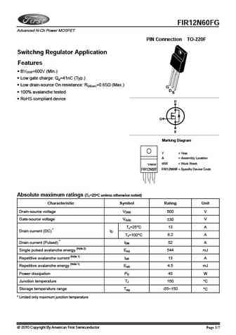
FIR12N60FG Advanced N-Ch Power MOSFET PIN Connection TO-220F Switchng Regulator Application Features BVDDS=600V (Min.) Low gate charge Qg=41nC (Typ.) Low drain-source On resistance RDS(on)=0.65 (Max.) G D S 100% avalanche tested RoHS compliant device D G S Marking Diagram Y = Year A = Assembly Location WW = Work Week YAWW FIR12N60F = Specif
smt12n60.pdf
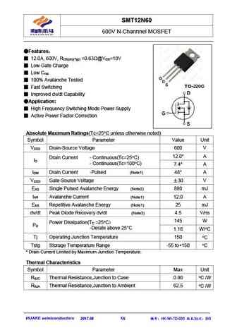
SMT12N60 600V N-Channnel MOSFET Features 12.0A, 600V, R =0.63 @V =10V DS(on)(Typ) GS Low Gate Charge Low C rss 100% Avalanche Tested Fast Switching Improved dv/dt Capability Application High Frequency Switching Mode Power Supply Active Power Factor Correction Absolute Maximum Ratings(Tc=25 C unless otherwise noted) Symbol Parameter Va
smf12n60.pdf
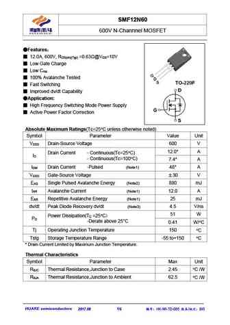
SMF12N60 600V N-Channnel MOSFET Features 12.0A, 600V, R =0.63 @V =10V DS(on)(Typ) GS Low Gate Charge Low C rss 100% Avalanche Tested Fast Switching Improved dv/dt Capability Application High Frequency Switching Mode Power Supply Active Power Factor Correction Absolute Maximum Ratings(Tc=25 C unless otherwise noted) Symbol Parameter Va
hf12n60.pdf
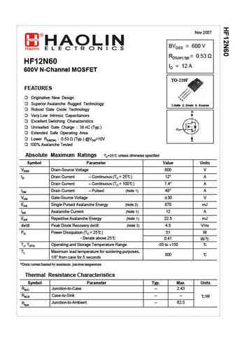
Nov 2007 BVDSS = 600 V RDS(on) typ = 0.53 HF12N60 ID = 12 A 600V N-Channel MOSFET TO-220F FEATURES 1 Originative New Design 2 3 Superior Avalanche Rugged Technology 1.Gate 2. Drain 3. Source Robust Gate Oxide Technology Very Low Intrinsic Capacitances Excellent Switching Characteristics Unrivalled Gate Charge 38 nC (Typ.) Extended Safe Operati
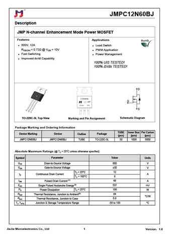
jmpf12n60bj.pdf
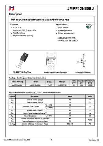
JMPF12N60BJ Description JMP N-channel Enhancement Mode Power MOSFET Features Applications 600V, 12A Load Switch RDS(ON)
jmpc12n60bj.pdf
JMPC12N60BJ Description JMP N-channel Enhancement Mode Power MOSFET Features Applications 600V, 12A Load Switch RDS(ON)
lnd12n60 lnc12n60 lne12n60 lnf12n60.pdf
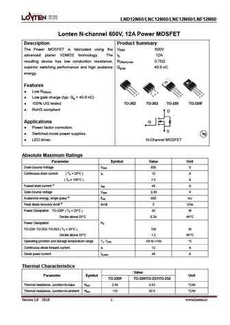
LND12N60/LNC12N60/LNE12N60/LNF12N60 Lonten N-channel 600V, 12A Power MOSFET Description Product Summary The Power MOSFET is fabricated using the VDSS 600V advanced planer VDMOS technology. The ID 12A resulting device has low conduction resistance, RDS(on),max 0.75 superior switching performance and high avalance Qg,typ 40.8 nC energy. Features Low RDS(on) Low gate
si12n60.pdf

N-CHANNEL MOSFET SI12N60 ABSOLUTE RATINGS (Tc=25 ) Value Parameter Symbol Unit SSS12N60 VDSS V 600 Drain-Source Voltage ID 12 A Drain Current -continuous T=25 1 IDM 48 A Drain Current - pulse note 1
hm12n60 hm12n60f.pdf
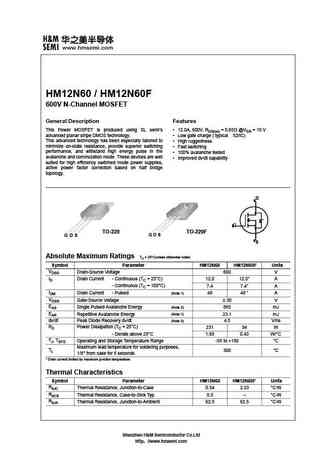
HM12N60 / HM12N60F 600V N-Channel MOSFET General Description Features This Power MOSFET is produced using SL semi s 12.0A, 600V, RDS(on) = 0.65 @VGS = 10 V advanced planar stripe DMOS technology. Low gate charge ( typical 52nC) This advanced technology has been especially tailored to High ruggedness minimize on-state resistance, provide superior switching Fast switc
fxn12n60fs.pdf
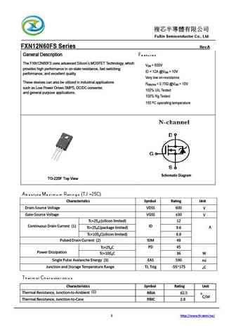
FuXin Semiconductor Co., Ltd. FXN12N60FS Series Rev.A General Description Features The FXN12N60FS uses advanced Silicon s MOSFET Technology, which V = 600V DS provides high performance in on-state resistance, fast switching ID = 12A @V = 10V GS performance, and excellent quality. Very low on-resistance These devices can also be utilized in i
h12n60p h12n60f.pdf
12N60 Series N-Channel MOSFET 12A, 600V, N H FQP12N60C H12N60P P TO-220AB HAOHAI 50Pcs 1000Pcs 5000Pcs 12N60 FQPF12N60C H12N60F F TO-220FP 12N60 Series Pin Assignment Features ID=12A Originative
aot12n60.pdf

isc N-Channel MOSFET Transistor AOT12N60 FEATURES Drain Current I =12A@ T =25 D C Drain Source Voltage- V =600V(Min) DSS Static Drain-Source On-Resistance R = 0.55 (Max) DS(on) 100% avalanche tested Minimum Lot-to-Lot variations for robust device performance and reliable operation DESCRIPTION Designed for use in switch mode power supplies and general purpos
12n60-263.pdf
INCHANGE Semiconductor Isc N-Channel MOSFET Transistor 12N60 FEATURES With To-263(D2PAK) package Low input capacitance and gate charge Low gate input resistance 100% avalanche tested Minimum Lot-to-Lot variations for robust device performance and reliable operation APPLICATIONS Switching applications Designed for high efficiency switch mode power supply ABSOLUTE
aotf12n60.pdf
isc N-Channel MOSFET Transistor AOTF12N60 FEATURES Drain Current I =12A@ T =25 D C Drain Source Voltage- V =600V(Min) DSS Static Drain-Source On-Resistance R = 0.55 (Max) DS(on) 100% avalanche tested Minimum Lot-to-Lot variations for robust device performance and reliable operation DESCRIPTION Designed for use in switch mode power supplies and general purpo
12n60.pdf
isc N-Channel Mosfet Transistor 12N60 FEATURES Drain Current I = 12A@ T =25 D C Drain Source Voltage- V = 600V (Min) DSS Static Drain-Source On-Resistance R = 0.7 (Max) DS(on) Avalanche Energy Specified Fast Switching Simple Drive Requirements Minimum Lot-to-Lot variations for robust device performance and reliable operation DESCRITION Designed for
aot12n60fd.pdf
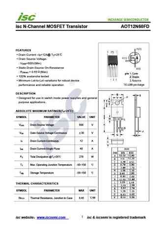
isc N-Channel MOSFET Transistor AOT12N60FD FEATURES Drain Current I =12A@ T =25 D C Drain Source Voltage- V =600V(Min) DSS Static Drain-Source On-Resistance R = 0.65 (Max) DS(on) 100% avalanche tested Minimum Lot-to-Lot variations for robust device performance and reliable operation DESCRIPTION Designed for use in switch mode power supplies and general purp
aotf12n60fd.pdf
isc N-Channel MOSFET Transistor AOTF12N60FD FEATURES Drain Current I =12A@ T =25 D C Drain Source Voltage- V =600V(Min) DSS Static Drain-Source On-Resistance R = 0.65 (Max) DS(on) 100% avalanche tested Minimum Lot-to-Lot variations for robust device performance and reliable operation DESCRIPTION Designed for use in switch mode power supplies and general pur
aob12n60fd.pdf
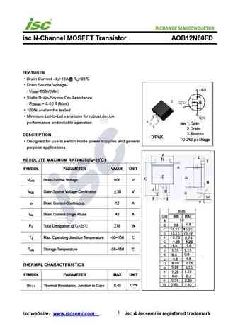
isc N-Channel MOSFET Transistor AOB12N60FD FEATURES Drain Current I =12A@ T =25 D C Drain Source Voltage- V =600V(Min) DSS Static Drain-Source On-Resistance R = 0.65 (Max) DS(on) 100% avalanche tested Minimum Lot-to-Lot variations for robust device performance and reliable operation DESCRIPTION Designed for use in switch mode power supplies and general purp
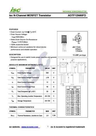
fqpf12n60c.pdf
isc N-Channel Mosfet Transistor FQPF12N60C FEATURES Drain Current I = 12A@ T =25 D C Drain Source Voltage- V = 600V(Min) DSS Static Drain-Source On-Resistance R = 0.65 (Max) DS(on) 100% avalanche tested Minimum Lot-to-Lot variations for robust device performance and reliable operation DESCRITION Designed for high efficiency switch mode power supply. A
aow12n60.pdf
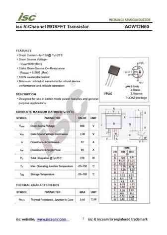
isc N-Channel MOSFET Transistor AOW12N60 FEATURES Drain Current I =12A@ T =25 D C Drain Source Voltage- V =600V(Min) DSS Static Drain-Source On-Resistance R = 0.55 (Max) DS(on) 100% avalanche tested Minimum Lot-to-Lot variations for robust device performance and reliable operation DESCRIPTION Designed for use in switch mode power supplies and general purpos
Другие IGBT... 12N60L-TF1-T, 12N60G-TF1-T, 12N60L-TF2-T, 12N60G-TF2-T, 12N60L-TF3-T, 12N60G-TF3-T, 12N60L-T2Q-T, 12N60G-T2Q-T, IRFP064N, 12N60G-T3P-T, 12N65KL-TA3-T, 12N65KG-TA3-T, 12N65KL-TF1-T, 12N65KG-TF1-T, 12N65KL-TF2-T, 12N65KG-TF2-T, 12N65KL-TF3-T
Параметры MOSFET. Взаимосвязь и компромиссы
History: CJBB3134K | 2N5640
🌐 : EN ES РУ

Список транзисторов
Обновления
MOSFET: MSH100N045SA | MSD60P16 | MSD40P45 | MSB100N023 | MS60P03 | MS40P05AU | MS40P05 | MS40N05 | MS34P07 | MS34P01 | MS23P03 | MS23N06A | BPMS04N003M | BPM0405CG | BPM0306CG | BP0405SCG
Popular searches
fb4410z | 2sa899 | 2sc1166 | jcs9n50fc datasheet | 2n2147 | 2sc870 | 2sa771 | d667