15N10L-TN3-R. Аналоги и основные параметры
Наименование производителя: 15N10L-TN3-R
Тип транзистора: MOSFET
Полярность: N
Предельные значения
Pd ⓘ - Максимальная рассеиваемая мощность: 34.7 W
|Vds|ⓘ - Максимально допустимое напряжение сток-исток: 100 V
|Vgs|ⓘ - Максимально допустимое напряжение затвор-исток: 20 V
|Id| ⓘ - Максимально допустимый постоянный ток стока: 14.7 A
Tj ⓘ - Максимальная температура канала: 150 °C
Электрические характеристики
tr ⓘ - Время нарастания: 33 ns
Cossⓘ - Выходная емкость: 58 pf
RDSonⓘ - Сопротивление сток-исток открытого транзистора: 0.1 Ohm
Тип корпуса: TO-252
Аналог (замена) для 15N10L-TN3-R
- подборⓘ MOSFET транзистора по параметрам
15N10L-TN3-R даташит
15n10l-tm3-t 15n10g-tm3-t 15n10l-tn3-r 15n10g-tn3-r.pdf
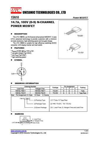
UNISONIC TECHNOLOGIES CO., LTD 15N10 Power MOSFET 14.7A, 100V (D-S) N-CHANNEL POWER MOSFET DESCRIPTION The UTC 15N10 is an N-Channel enhancement MOSFET, it uses UTC s advanced technology to provide customers with a minimum on-state resistance, high switching speed and low gate charge. The UTC 15N10 is suitable for high efficiency switching DC/DC converter, LCD display in
fir15n10lg.pdf
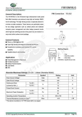
FIR15N10LG N-Channel 100V(D-S) MOSFET PIN Connection TO-252 General Description The FIR15N10LG is the N-Channel logic enhancement mode power field effect transistors are produced using high cell density, DMOS trench technology. This high density process is especially tailored to minimize on-state resistance. These devices are particularly suited for low voltage application such as c
agm015n10ll.pdf
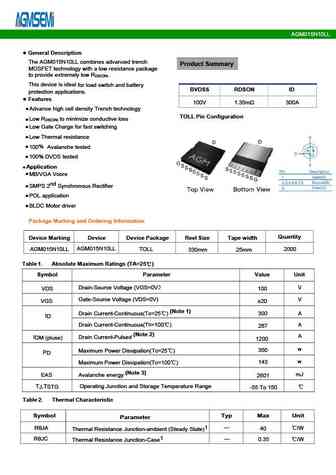
AGM015N10LL TOLL Marking Instructions www.agm-mos.com 7 VER2.71 AGM015N10LL Disclaimer The information provided in this document is believed to be accurate and reliable. However,Shenzhen Core Control Source Electronics Technology Co., Ltd. does not assume any responsibility for the following consequences.Do not consider the use of such information or use beyond its scope. The

mte215n10e.pdf
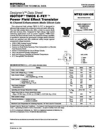
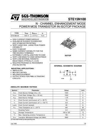
MOTOROLA Order this document SEMICONDUCTOR TECHNICAL DATA by MTE215N10E/D Designer's Data Sheet MTE215N10E ISOTOP TMOS E-FET. Motorola Preferred Device Power Field Effect Transistor N Channel Enhancement Mode Silicon Gate TMOS POWER FET 215 AMPERES This advanced high voltage TMOS E FET is designed to 100 VOLTS withstand high energy in the avalanche mode and switch e
sth315n10f7-2 sth315n10f7-6.pdf
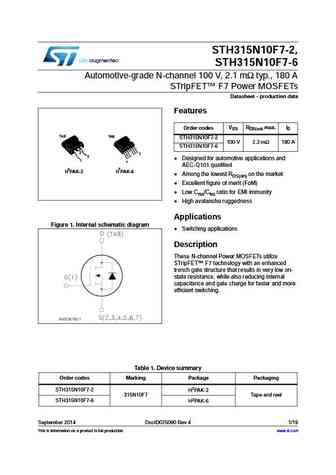
STH315N10F7-2, STH315N10F7-6 Automotive-grade N-channel 100 V, 2.1 m typ., 180 A STripFET F7 Power MOSFETs Datasheet - production data Features VDS RDS(on) max. ID Order codes TAB TAB STH315N10F7-2 100 V 2.3 m 180 A STH315N10F7-6 2 7 3 Designed for automotive applications and 1 1 AEC-Q101 qualified 2 2 H PAK-6 H PAK-2 Among the lowest RDS(on) on the marke
stp315n10f7.pdf
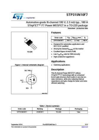
STP315N10F7 Automotive-grade N-channel 100 V, 2.3 m typ., 180 A STripFET F7 Power MOSFET in a TO-220 package Datasheet - production data Features VDS RDS(on) max. ID Order code TAB STP315N10F7 100 V 2.7 m 180 A Designed for automotive applications and AEC-Q101 qualified 3 2 Among the lowest RDS(on) on the market 1 Excellent figure of merit (FoM) TO-220
rtp315n10f7.pdf
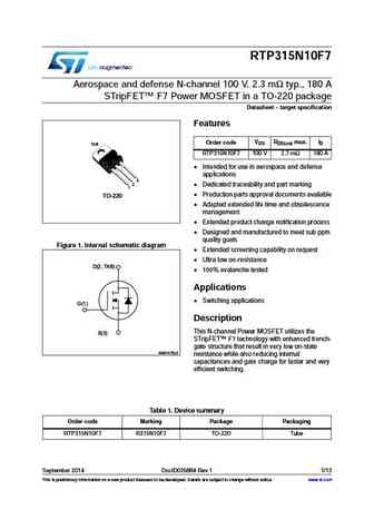
RTP315N10F7 Aerospace and defense N-channel 100 V, 2.3 m typ., 180 A STripFET F7 Power MOSFET in a TO-220 package Datasheet - target specification Features VDS RDS(on) max. ID Order code TAB RTP315N10F7 100 V 2.7 m 180 A Intended for use in aerospace and defense applications 3 2 Dedicated traceability and part marking 1 Production parts approval documents av
ipt015n10n5.pdf
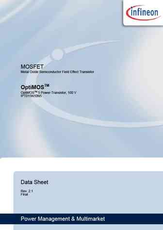
MOSFET Metal Oxide Semiconductor Field Effect Transistor OptiMOSTM OptiMOSTM 5 Power-Transistor, 100 V IPT015N10N5 Data Sheet Rev. 2.1 Final Power Management & Multimarket OptiMOSTM 5 Power-Transistor, 100 V IPT015N10N5 HSOF 1 Description Features Tab Ideal for high frequency switching and sync. rec. Excellent gate charge x R product (FOM) DS(on) Very low on-resis
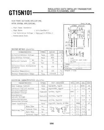
ixgp15n100c.pdf

VCES =1000 V IXGA 15N100C IGBT IC25 = 30 A IXGP 15N100C VCE(sat) = 3.5 V Lightspeed Series tfi(typ) = 115 ns Symbol Test Conditions Maximum Ratings VCES TJ = 25 C to 150 C 1000 V TO-220AB (IXGP) VCGR TJ = 25 C to 150 C; RGE = 1 M 1000 V VGES Continuous 20 V VGEM Transient 30 V G C E IC25 TC = 25 C30 A IC90 TC = 90 C15 A ICM TC = 25 C, 1 ms 60 A TO-263 AA (IXGA)
ixga15n100c ixgp15n100c.pdf
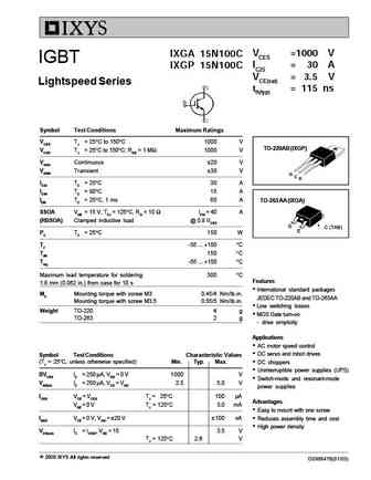
VCES =1000 V IXGA 15N100C IGBT IC25 = 30 A IXGP 15N100C VCE(sat) = 3.5 V Lightspeed Series tfi(typ) = 115 ns Symbol Test Conditions Maximum Ratings VCES TJ = 25 C to 150 C 1000 V TO-220AB (IXGP) VCGR TJ = 25 C to 150 C; RGE = 1 M 1000 V VGES Continuous 20 V VGEM Transient 30 V G C E IC25 TC = 25 C30 A IC90 TC = 90 C15 A ICM TC = 25 C, 1 ms 60 A TO-263 AA (IXGA)
ixfh14n100 ixft14n100 ixfx14n100 ixfh15n100 ixft15n100 ixfx15n100.pdf
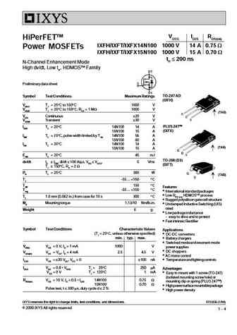
VDSS ID25 RDS(on) HiPerFETTM IXFH/IXFT/IXFX14 N100 1000 V 14 A 0.75 W Power MOSFETs IXFH/IXFT/IXFX15 N100 1000 V 15 A 0.70 W trr 200 ns N-Channel Enhancement Mode High dv/dt, Low trr, HDMOSTM Family Preliminary data sheet TO-247 AD Symbol Test Conditions Maximum Ratings (IXFH) VDSS TJ = 25 C to 150 C 1000 V VDGR TJ = 25 C to 150 C; RGS = 1 MW 1000 V (TAB) VGS Continuous
mcq15n10y.pdf
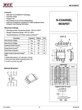
MCQ15N10Y Features Split Gate Trench MOSFET Technology Low Gate Charge Halogen Free Epoxy Meets UL 94 V-0 Flammability Rating N-CHANNEL Lead Free Finish/RoHS Compliant ("P" Suffix Designates RoHS Compliant. See Ordering Information) MOSFET Maximum Ratings Operating Junction Temperature Range -55 C to +150 C Storage Temperature Range -55 C to +150 C
mcq15n10b.pdf
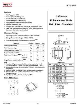
MCQ15N10B Features Low RDS(on) and FOM N-Channel Extremely Low Switching Loss Excellent Stability and Uniformity Fast Switching and Soft Recovery Enhancement Mode Epoxy Meets UL 94 V-0 Flammability Rating Moisture Sensitivity Level 1 Field Effect Transistor Halogen Free Available Upon Request By Adding Suffix "-HF" Lead Free Finish/RoHS Compliant ("P
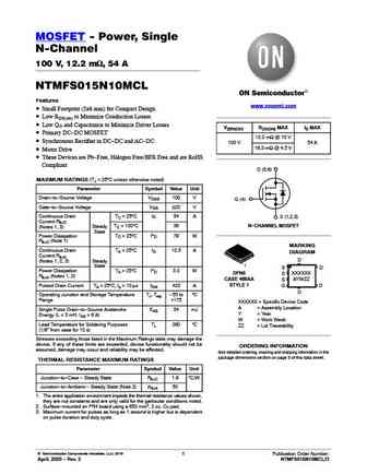
nvmfs015n10mcl.pdf
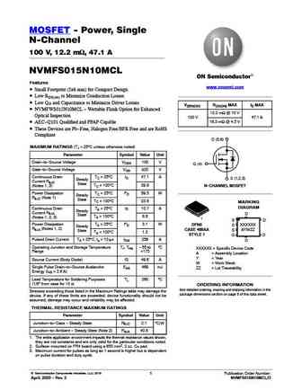
MOSFET - Power, Single N-Channel 100 V, 12.2 mW, 47.1 A NVMFS015N10MCL Features www.onsemi.com Small Footprint (5x6 mm) for Compact Design Low RDS(on) to Minimize Conduction Losses Low QG and Capacitance to Minimize Driver Losses V(BR)DSS RDS(ON) MAX ID MAX NVMFWS015N10MCL - Wettable Flank Option for Enhanced 12.2 mW @ 10 V Optical Inspection 100 V 47.1 A 18.3 mW @
ssd15n10.pdf
SSD15N10 15A, 100V, RDS(ON) 110m N-Ch Enhancement Mode Power MOSFET Elektronische Bauelemente RoHS Compliant Product A suffix of -C specifies halogen free TO-252(D-Pack) DESCRIPTION The SSD15N10 provide the designer with the best combination of fast switching. The TO-252 package is universally preferred for all commercial-industrial surface mount applications. The
g15n10c.pdf
GOFORD G15N10C General Description The G15N10C combines advanced trench MOSFET technology with a low resistance package to provide extremely low RDS(ON). This device is ideal for power switching application and LED backlighting. Features RDS(ON) VDSS ID @10V (typ) Schematic Diagram 100V 15A 70 m Ultra Low On-Resistance High UIS and UIS 100% Test Applic
gt15n10s.pdf
GOFORD GT15N10S N-Channel Enhancement Mode Power MOSFET Description The GT15N10S uses advanced trench technology to provide excellent RDS(ON) , low gate charge. It can be used in a wide variety of applications. General Features Schematic diagram VDS 100V ID (at VGS = 10V) 10A RDS(ON) (at VGS = 10V)
brd15n10.pdf
BRD15N10 Rev.F Oct.-2018 DATA SHEET / Descriptions TO-252 N MOS N-CHANNEL MOSFET in a TO-252 Plastic Package. / Features R C DS(on) rss Low RDS(on),low gate charge, low Crss, fast switching. / Applications DC/DC
ndt15n10.pdf
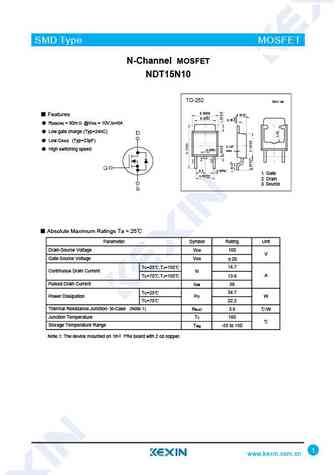
SMD Type MOSFET N-Channel MOSFET NDT15N10 TO-252 Unit mm +0.15 6.50-0.15 +0.1 Features 2.30 -0.1 +0.2 5.30-0.2 +0.8 0.50 -0.7 RDS(ON) = 80m @VGS = 10V,ID=8A Low gate charge (Typ=24nC) Low CRSS (Typ=23pF) 0.127 +0.1 High switching speed 0.80-0.1 max + 0.1 2.3 0.60- 0.1 1. Gate +0.15 4 .60 -0.15 2. Drain Source 3. Absolute Maximum Ratin
me15n10 me15n10g.pdf
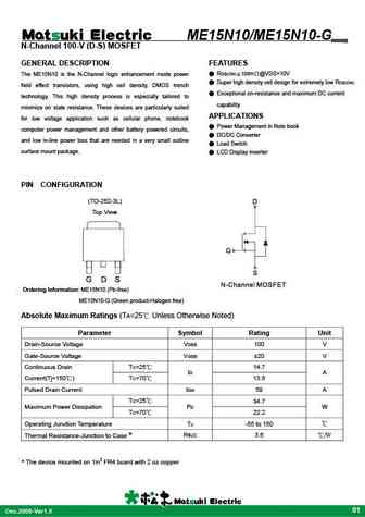
ME15N10/ME15N10-G N-Channel 100-V (D-S) MOSFET GENERAL DESCRIPTION FEATURES RDS(ON) 100m @VGS=10V The ME15N10 is the N-Channel logic enhancement mode power Super high density cell design for extremely low RDS(ON) field effect transistors, using high cell density, DMOS trench Exceptional on-resistance and maximum DC current technology. This high density process is
me15n10 me15n10-g.pdf
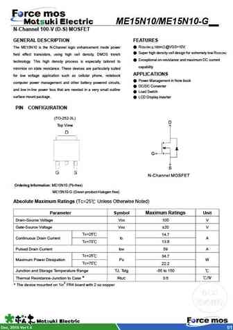
ME15N10/ME15N10-G N-Channel 100-V (D-S) MOSFET GENERAL DESCRIPTION FEATURES RDS(ON) 100m @VGS=10V The ME15N10 is the N-Channel logic enhancement mode power Super high density cell design for extremely low RDS(ON) field effect transistors, using high cell density, DMOS trench Exceptional on-resistance and maximum DC current technology. This high density process is
mee15n10-g.pdf
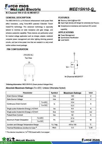
MEE15N10-G N-Channel 100-V (D-S) MOSFET GENERAL DESCRIPTION FEATURES RDS(ON) 100m @VGS=10V The MEE15N10-G is a N-Channel enhancement mode power field Super high density cell design for extremely low RDS(ON) effect transistors, using Force-MOS patented Extended Trench Exceptional on-resistance and maximum DC current Gate(ETG) technology. This advanced technology is esp
sl15n10a.pdf
SL15N10A N-Channel Enhancement Mode Field Effect Transistor Product Summary V 100V DS I 15A D R ( at V = 10V) 115mohm DS(ON) GS R ( at V = 4.5V) 1 0mohm DS(ON) GS 100% UIS Tested 100% VDS Tested General Description Trench Power MV MOSFET technology Excellent package for heat dissipation High density cell design for low R DS(ON) Ap
15n10.pdf
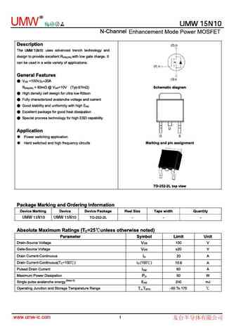
R UMW UMW 15N10 UMW 15N10 UMW 15N10 =20A UMW 15N10 UMW 15N10 20 www.umw-ic.com 1 R UMW UMW 15N10 UMW 15N10 20 www.umw-ic.com 2 R UMW UMW 15N10 UMW 15N10 www.umw-ic.com 3 R UMW UMW 15N10 UMW 15N10 www.umw-ic.com 4 R UMW UMW 15N10 UMW 15N10 www.umw-ic.com
wmo15n10t1.pdf
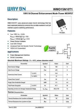
WMO15N10T1 100V N-Channel Enhancement Mode Power MOSFET Description WMO15N10T1 uses advanced power trench technology that has been especially tailored to minimize the on-state resistance and yet D maintain superior switching performance. S G Features TO-252 V = 100V, I = 14.6A DS D R
ap15n10.pdf
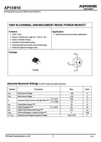
AP15N10 DATA SHEET DATA SHEET N-Channel Enhancement Mode Power MOSFET 100V N-CHANNEL ENHANCEMENT MODE POWER MOSFET Features Application 100V, 14.6A Synchronous buck converter applications. R =100m (max.) @ V = 10V, I = 5A DS(ON) GS D Super Low Gate Charge Excellent CdV/dt effect decline Advanced high cell density Trench technology RoHS Complia
ptd15n10.pdf
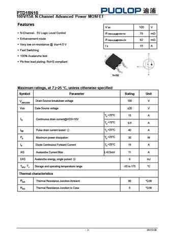
PTD15N10 100V/15A N-Channel Advanced Power MOSFET Features V DS 100 V N-Channel 5V Logic Level Control R DS(on),typ@VGS=10V 78 m Enhancement mode R DS(on),typ@VGS=4.5V 82 m Very low on-resistance @ VGS=4.5 V I D 15 A Fast Switching 100% Avalanche test Pb-free lead plating; RoHS compliant To-252 Maximum ratings, at T j=25 C, unless otherw
agm15n10d-g.pdf
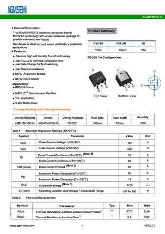
AGM15N10D-G General Description Product Summary The AGM15N10D-G combines advanced trench to MOSFET technology with a low resistance package provide extremely low R DS(ON) BVDSS RDSON ID This device is ideal for load switch and battery protection applications. 100V 68m 16A Features Advance high cell density Trench technology TO-252 Pin Configuration Low R to minimiz
agm15n10ap.pdf
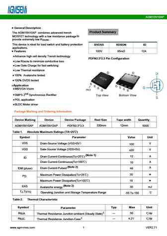
AGM15N10AP General Description Product Summary The AGM15N10AP combines advanced trench to MOSFET technology with a low resistance package provide extremely low R . DS(ON) This device is ideal load switch and battery protection for BVDSS RDSON ID applications. Features 100V 85m 12A Advance high cell density Trench technology PDFN3.3*3.3 Pin Configuration Low R
agm15n10d.pdf
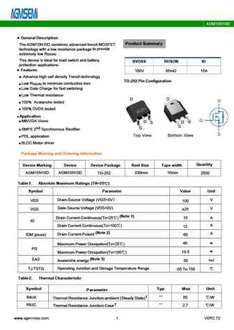
AGM15N10D General Description Product Summary The AGM15N10D combines advanced trench MOSFET to provide technology with a low resistance package extremely low R DS(ON) This device is ideal and battery for load switch BVDSS RDSON ID protection applications. Features 100V 85m 15A Advance high cell density Trench technology TO-252 Pin Configuration Low R to minimize co
tx15n10b.pdf
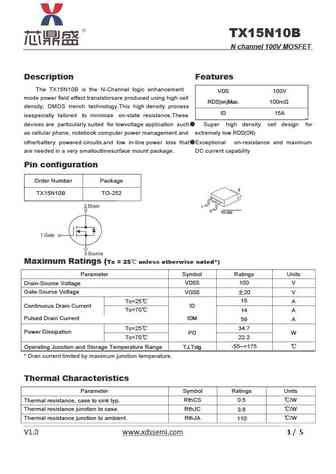
TX15N10B N channel 100V MOSFET Description Features The TX15N10B is the N-Channel logic enhancement VDS 100V mode power field effect transistorsare produced using high cell RDS(on)Max. 100m density, DMOS trench technology.This high density process ID 15A isespecially tailored to minimize on-state resistance.These devices are particularly suited for lowvoltage application such Sup
hgt015n10s.pdf
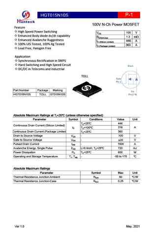
HGT015N10S P-1 100V N-Ch Power MOSFET Feature High Speed Power Switching 100 V VDS Enhanced Body diode dv/dt capability 1.3 RDS(on),typ mW Enhanced Avalanche Ruggedness 446 A ID (Sillicon Limited) 100% UIS Tested, 100% Rg Tested 360 A ID (Package Limited) Lead Free, Halogen Free Application Synchronous Rectification in SMPS Hard Switching and High S
15n10b.pdf
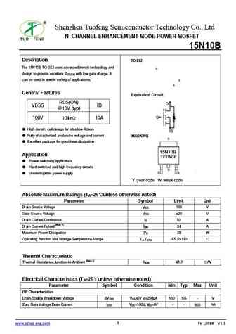
Shenzhen Tuofeng Semiconductor Technology Co., Ltd N -CHANNEL ENHANCEMENT MODE POWER MOSFET 15N10B Description TO-252 The 15N10B TO-252 uses advanced trench technology and D design to provide excellent R with low gate charge. It DS(ON) can be used in a wide variety of applications. S G General Features Equivalent Circuit RDS(ON) D VDSS ID @10V (typ) G 100V 10A 104
15n10.pdf
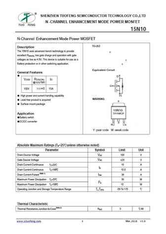
SHENZHEN TUOFENG SEMICONDUCTOR TECHNOLOGY CO.,LTD N -CHANNEL ENHANCEMENT MODE POWER MOSFET 15N10 N-Channel Enhancement Mode Power MOSFET TO-252 Description The 15N10 uses advanced trench technology to provide D excellent RDS(ON), low gate charge and operation with gate voltages as low as 4.5V. This device is suitable for use as a S Battery protection or in other switching app
wsf15n10g.pdf
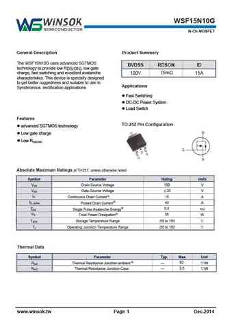
WSF15N10G N-Ch MOSFET Product Summery General Description The WSF15N10G uses advanced SGTMOS BVDSS RDSON ID technology to provide low RDS(ON), low gate charge, fast switching and excellent avalanche 75m 15A 100V characteristics. This device is specially designed to get better ruggedness and suitable to use in Applications Synchronous rectification applications Fast Swi
wsf15n10a.pdf
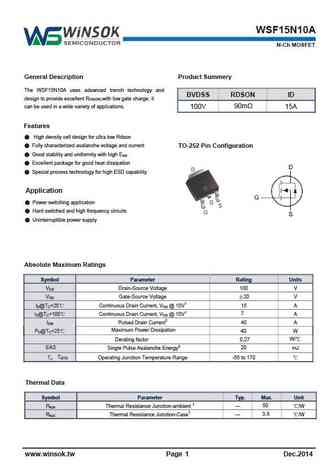
WSF15N10A N-Ch MOSFET Product Summery General Description The WSF15N10A uses advanced trench technology and BVDSS RDSON ID design to provide excellent R with low gate charge. It DS(ON) can be used in a wide variety of applications. 100V 90m 15A Features High density cell design for ultra low Rdson Fully characterized avalanche voltage and current TO-252 Pin Configu
wsc15n10.pdf
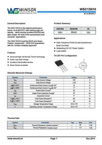
WSC15N10 N-Ch MOSFET Product Summery General Description The WSC15N10 is the highest performance BVDSS RDSON ID trench N-ch MOSFET with extreme high cell density , which provide excellent RDSON and 100V 80m 15A gate charge for most of the synchronous buck converter applications . Applications The WSC15N10 meet the RoHS and Green High Frequency Point-of-Load Synchronous
wsf15n10.pdf
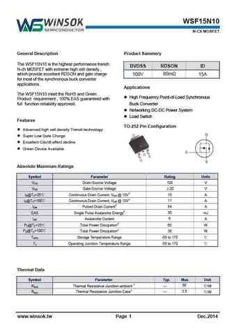
WSF15N10 N-Ch MOSFET Product Summery General Description The WSF15N10 is the highest performance trench BVDSS RDSON ID N-ch MOSFET with extreme high cell density , which provide excellent RDSON and gate charge 100V 80m 15A for most of the synchronous buck converter applications . Applications The WSF15N10 meet the RoHS and Green High Frequency Point-of-Load Synchronous
vbze15n10.pdf
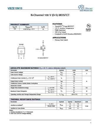
VBZE15N10 www.VBsemi.com N-Channel 100 V (D-S) MOSFET FEATURES PRODUCT SUMMARY TrenchFET Power MOSFET VDS (V) RDS(on) ( )ID (A) 175 C Junction Temperature 100 at VGS = 10 V 0.097 16 PWM Optimized 100 % Rg Tested Compliant to RoHS Directive 2002/95/EC APPLICATIONS Primary Side Switch D TO-252 G S G D S N-Channel MOSFET ABSOLUTE MAXIMUM RATING
vbzfb15n10.pdf
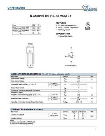
VBZFB15N10 www.VBsemi.com N-Channel 100 V (D-S) MOSFET FEATURES V VDS 100 DT-Trench Power MOSFET 175 C Junction Temperature RDS(on),typ VGS=10V m 115 100 % Rg Tested RDS(on),typ VGS=4.5V m 120 15 A ID APPLICATIONS Primary Side Switch TO-251 D G S G D S N-Channel MOSFET Top View ABSOLUTE MAXIMUM RATINGS (TC = 25 C, unless otherwise noted) Param
15n10-to251.pdf
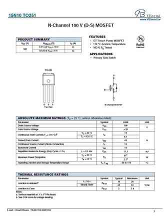
15N10 TO251 www.VBsemi.tw N-Channel 100 V (D-S) MOSFET FEATURES PRODUCT SUMMARY DT-Trench Power MOSFET VDS (V) RDS(on) ( )ID (A) 175 C Junction Temperature 0.115 at VGS = 10 V 15 100 % Rg Tested 100 0.120 at VGS = 6 V 15 APPLICATIONS Primary Side Switch TO-251 D G S G D S N-Channel MOSFET Top View ABSOLUTE MAXIMUM RATINGS (TC = 25 C, unless otherwi
me15n10.pdf
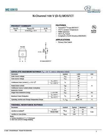
ME15N10 www.VBsemi.tw N-Channel 100 V (D-S) MOSFET FEATURES PRODUCT SUMMARY TrenchFET Power MOSFET VDS (V) RDS(on) ( )ID (A) 175 C Junction Temperature 100 0.11 4 at VGS = 10 V 15 PWM Optimized 100 % Rg Tested Compliant to RoHS Directive 2002/95/EC APPLICATIONS Primary Side Switch D TO-252 G S G D S N-Channel MOSFET ABSOLUTE MAXIMUM RATINGS (
yjd15n10a.pdf
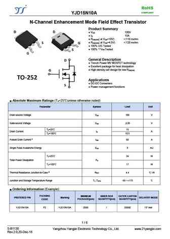
RoHS COMPLIANT YJD15N10A N-Channel Enhancement Mode Field Effect Transistor Product Summary V 100V DS I 15A D R ( at V =10V) 110 mohm DS(ON) GS R ( at V =4.5V) 120 mohm DS(ON) GS 100% UIS Tested 100% VDS Tested General Description Trench Power MV MOSFET technology Excellent package for heat dissipation High density ce
tsb15n10a.pdf
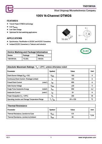
TSB15N10A Wuxi Unigroup Microelectronics Company 100V N-Channel DTMOS FEATURES Trench Power DTMOS technology Low RDS(ON) Low Gate Charge Optimized for fast-switching applications APPLICATIONS Synchronous Rectification in DC/DC and AC/DC Converters Isolated DC/DC Converters in Telecom and Industrial Device Marking and Package Information Device Pa
tsp15n10a.pdf
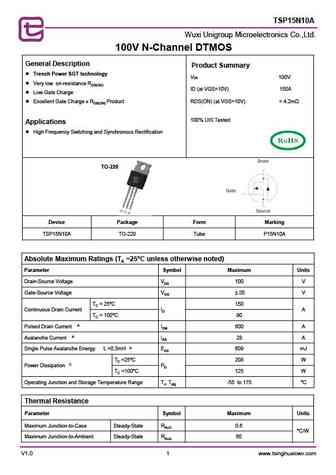
TSP15N10A Wuxi Unigroup Microelectronics Co.,Ltd. 100V N-Channel DTMOS General Description Product Summary Trench Power SGT technology VDS 100V Very low on-resistance RDS(ON) ID (at VGS=10V) 150A Low Gate Charge Excellent Gate Charge x RDS(ON) Product RDS(ON) (at VGS=10V)
hm15n10d.pdf
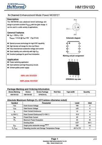
HM15N10D N-Channel Enhancement Mode Power MOSFET Description The HM15N10D uses advanced trench technology and design to provide excellent RDS(ON) with low gate charge. It can be used in a wide variety of applications. General Features VDS = 100V,ID =15A RDS(ON)
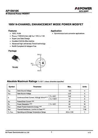
hm15n10k.pdf
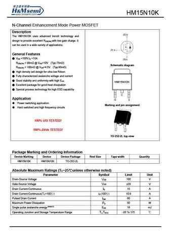
HM15N10K N-Channel Enhancement Mode Power MOSFET Description The HM15N10K uses advanced trench technology and design to provide excellent RDS(ON) with low gate charge. It can be used in a wide variety of applications. General Features VDS =100V,ID =15A RDS(ON)
mdt15n10.pdf
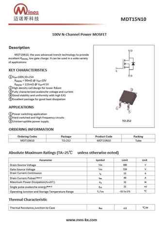
100V N-Channel Power MOSFET Description MDT15N10, the uses advanced trench technology to provide excellent R , low gate charge. It can be used in a wide variety DS(ON) of applications KEY CHARACTERISTICS V =100V,ID=15A DS R
h15n10u h15n10d.pdf
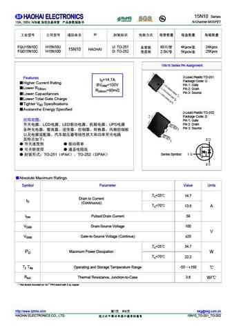
15N10 Series N-Channel MOSFET 15A, 100V, N H FQU15N10C H15N10U U TO-251 80 / 4Kpcs/ 24Kpcs HAOHAI 15N10 FQD15N10C H15N10D D TO-252 25Kpcs 2.5K/ 5Kpcs/ 15N10 Series Pin Assignment 3-Lead Plastic TO-2
stp315n10f7.pdf
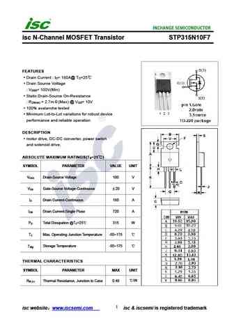
isc N-Channel MOSFET Transistor STP315N10F7 FEATURES Drain Current I = 180A@ T =25 D C Drain Source Voltage V = 100V(Min) DSS Static Drain-Source On-Resistance R = 2.7m (Max) @ V = 10V DS(on) GS 100% avalanche tested Minimum Lot-to-Lot variations for robust device performance and reliable operation DESCRIPTION motor drive, DC-DC converter, power switch and s
ap15n10d-l.pdf
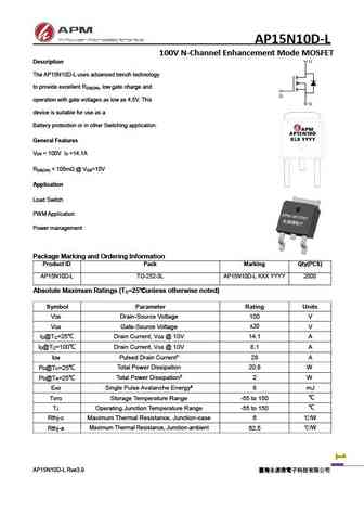
AP15N10D-L 100V N-Channel Enhancement Mode MOSFET Description The AP15N10D-L uses advanced trench technology to provide excellent R , low gate charge and DS(ON) operation with gate voltages as low as 4.5V. This device is suitable for use as a Battery protection or in other Switching application. General Features V = 100V I =14.1A DS D R
ap15n10s.pdf
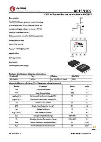
AP15N10S 100V N-Channel Enhancement Mode MOSFET Description The AP15N10S uses advanced trench technology to provide excellent R , low gate charge and DS(ON) operation with gate voltages as low as 4.5V. This device is suitable for use as a Battery protection or in other Switching application. General Features V = 100V I =15A DS D R
ap15n10y.pdf
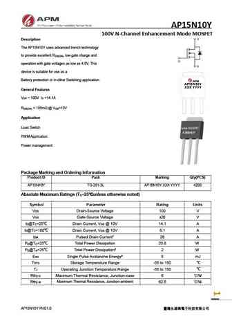
AP15N10Y 100V N-Channel Enhancement Mode MOSFET Description The AP15N10Y uses advanced trench technology to provide excellent R , low gate charge and DS(ON) operation with gate voltages as low as 4.5V. This device is suitable for use as a Battery protection or in other Switching application. General Features V = 100V I =14.1A DS D R
ap15n10d.pdf
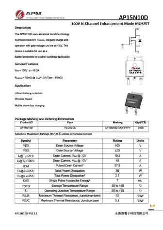
AP15N10D 100V N-Channel Enhancement Mode MOSFET Description The AP15N10D uses advanced trench technology to provide excellent R , low gate charge and DS(ON) operation with gate voltages as low as 4.5V. This device is suitable for use as a Battery protection or in other Switching application. General Features V = 100V I =19.3A DS D R
Другие IGBT... 14N50L-TQ2-R, 14N50G-TQ2-R, 14N50L-TF3-T, 14N50G-TF3-T, 14N50L-T3P-T, 14N50G-T3P-T, 15N10L-TM3-T, 15N10G-TM3-T, IRF730, 15N10G-TN3-R, 15N65L-T47-T, 15N65G-T47-T, 15N65L-TA3-T, 15N65G-TA3-T, 15N65L-TC3-T, 15N65G-TC3-T, 15N65L-TF1-T
History: 10N80G-TF2-T | 10N70L-TF1-T | 2N5116 | 19N10L-TMS2-T | 25N10 | 2N65M
🌐 : EN ES РУ

Список транзисторов
Обновления
MOSFET: AUW033N08BG | AUW025N10 | AUR030N10 | AUR020N10 | AUR020N085 | AUR014N10 | AUP074N10 | AUP065N10 | AUP062N08BG | AUP060N08AG | HYG053N10NS1B | HYG053N10NS1P | AP220N04T | AP220N04P | QM3126M3 | AUP060N055
Popular searches
2sc2383 | c3198 transistor | irfb3607pbf datasheet | 60n60 | 2n5485 equivalent | 2sa1941 | 2sc485 | 2sd287